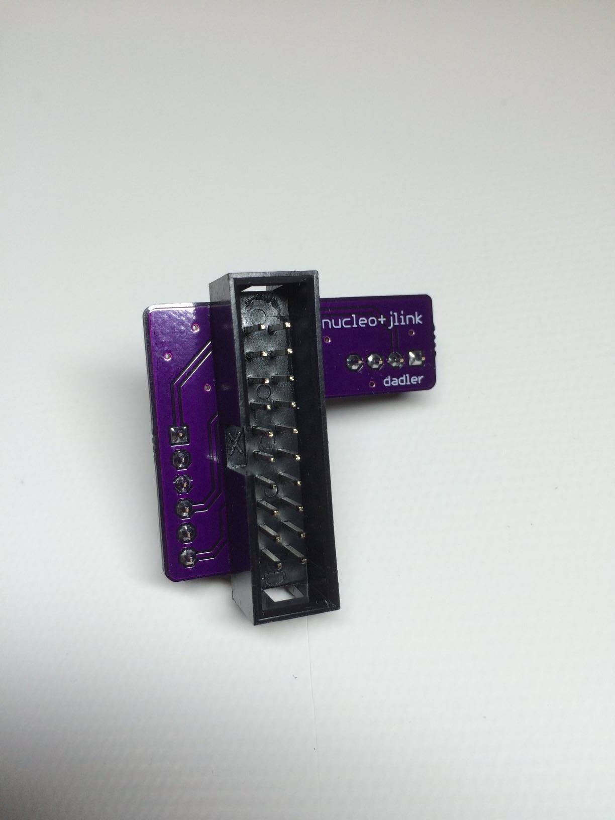
I wanted to use my SEGGER Jlink with my ST Nucleo dev boards, so I made an adapter:
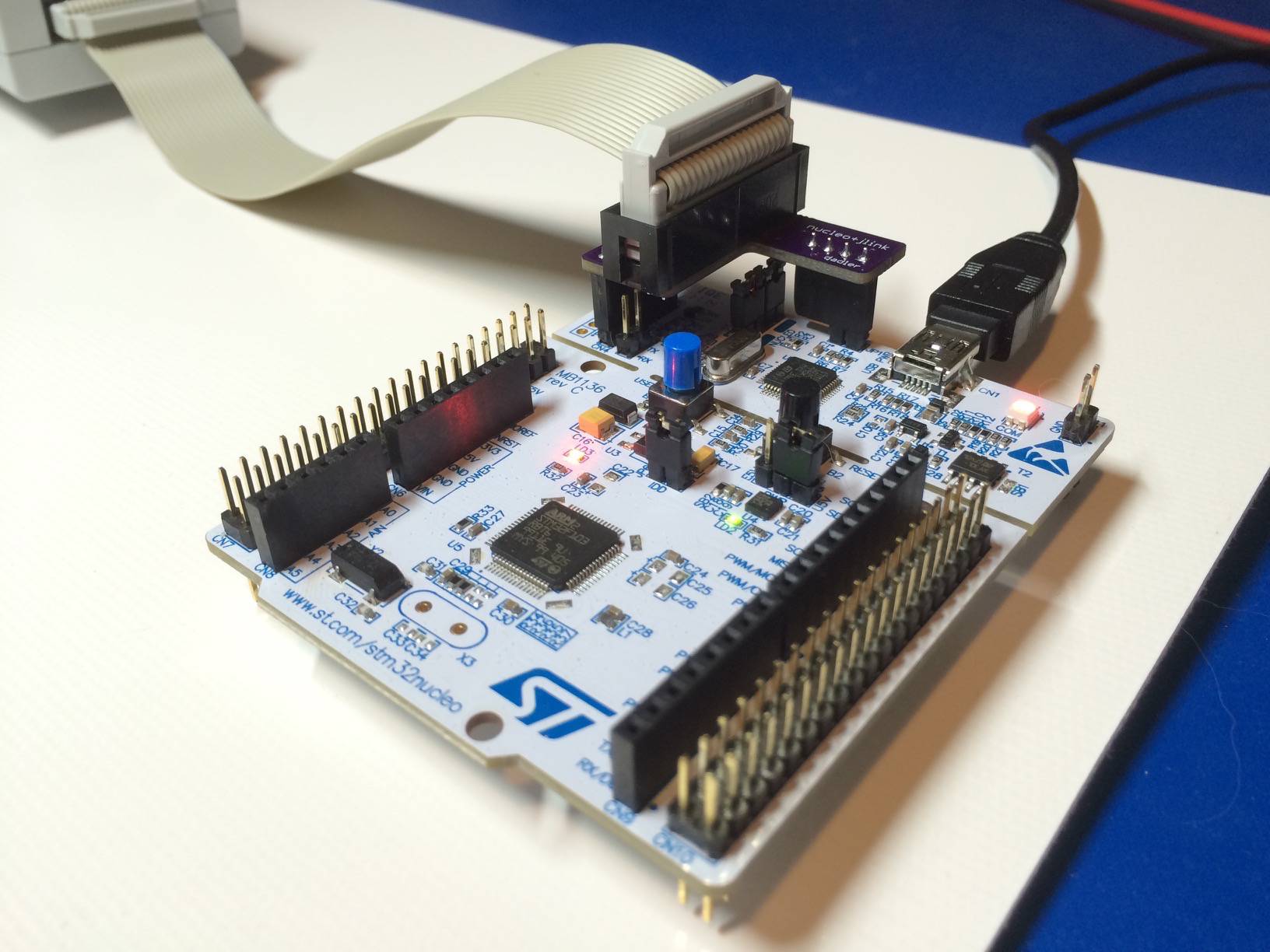
There are a bunch of different ways this could have been done, but I wanted a single adapter board and way of tapping into the target Vref without additional flying leads.
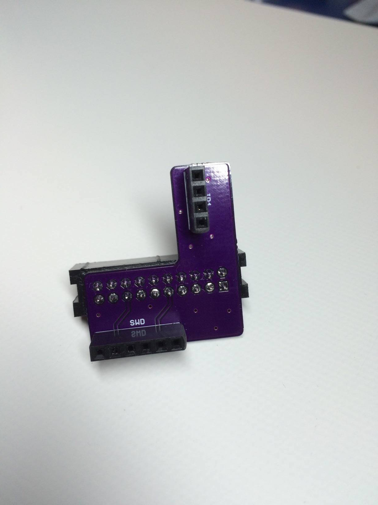
For some reason, ST populated D1 (BAT60JFILM) and R1 (10k pulldown), but left R9 unpopulated. Even if you populate R9, the other side is connected to AIN_1, which is a 4k7/4k7 potential divider from 3.3V and hence sits at ~1.65V. I'm not sure what the plan was here, but I decided to tap into 3.3V without modifying the board.
On the adapter, target Vref is tapped into JP1 (3.3V) on the Nucleo PCB, which is left open from the factory. JP1 controls the max current requested during USB enumeration. You may need to short it if you are powering the board via USB without enumeration. If you wish to short this jumper, use extended-length header pins or simply bridge the pins on the adapter PCB.
On the adapter, I connected pin 1 of the SWD connector (CN4) to target Vref, but this was unnecessary. It just felt like the right thing to do. Hehe.
Anyways, if you are interested in the layout files they are here:
https://github.com/dustinadler/nucleo-jlinkThe board is available on OSH Park:
https://oshpark.com/shared_projects/m3tkYXXRMore pictures: