-
What's the fastest clock you have generated on a GPIO pin of an ARM dev board
Posted by photon on 30 Dec, 2015 02:53 -
Has anyone been able to bit bang a 20 MHz clock on any arm dev board ? If so, could you share your arm board. I would like this to be done with a program, rather than assembly code, and look like:
while(1) {
write GPIO 1;
write GPIO 0;
}
-
C vs Assembly vs Verilog:
In other words, use hardware not software
Edit: I can get 80MHz using a clock instance module (controlled by software) and using an external precise clock
http://www.cypress.com/file/127816/download
on this prototyping board:
http://www.cypress.com/documentation/development-kitsboards/cy8ckit-059-psoc-5lp-prototyping-kit-onboard-programmer-and
-
On the LPCLink2 you can toggle GPIO at core speed (ie, above code compiles to three instructions/four cycles in the loop then 204MHz/4) from recollection if you run your code from RAM and ensure instructions are word aligned. You can also see the 204MHz clock frequency if you configure the clock routing appropriately.
-
Setting -O3 optimization, this generates a 50.5MHz toggle on the LPCLink2.Code: [Select]
#define LED0_PORT  0
#define LED0_PIN   8

int main(void)
{
	LPC_GPIO_T *pGPIO=(LPC_GPIO_T *)0x400F4000;

	SystemCoreClockUpdate();
	Board_Init();

	while (1)
	{
		pGPIO->B[LED0_PORT][LED0_PIN] = 1;
		pGPIO->B[LED0_PORT][LED0_PIN] = 0;
	}

	return 0;
} -
Setting -O3 optimization, this generates a 50.5MHz toggle on the LPCLink2.
That is the fastest I have heard of with a C program. What was the speed difference between -O0 (default) and -O3? I assume gcc compiler?Code: [Select]#define LED0_PORT 0
#define LED0_PIN 8
int main(void)
{
LPC_GPIO_T *pGPIO=(LPC_GPIO_T *)0x400F4000;
SystemCoreClockUpdate();
Board_Init();
while (1)
{
pGPIO->B[LED0_PORT][LED0_PIN] = 1;
pGPIO->B[LED0_PORT][LED0_PIN] = 0;
}
return 0;
} -
C vs Assembly vs Verilog:
In other words, use hardware not software
Edit: I can get 80MHz using a clock instance module (controlled by software) and using an external precise clock
http://www.cypress.com/file/127816/download
on this prototyping board:
http://www.cypress.com/documentation/development-kitsboards/cy8ckit-059-psoc-5lp-prototyping-kit-onboard-programmer-and
That is a good video and interesting technique! I have heard of FPGA compilers for C programs but did not know if the implementations were far enough along to be useful. Is there a way in PSOC to express the RTL in C? I am wondering how to run something that is expressed partially in C and partially in RTL. -
C vs Assembly vs Verilog:
In other words, use hardware not software
Edit: I can get 80MHz using a clock instance module (controlled by software) and using an external precise clock
http://www.cypress.com/file/127816/download
on this prototyping board:
http://www.cypress.com/documentation/development-kitsboards/cy8ckit-059-psoc-5lp-prototyping-kit-onboard-programmer-and
That is a good video and interesting technique! I have heard of FPGA compilers for C programs but did not know if the implementations were far enough along to be useful. Is there a way in PSOC to express the RTL in C? I am wondering how to run something that is expressed partially in C and partially in RTL.
Maybe not with the flipflop and the not gate, but they do have frequency dividers or the clock that is totally programmable.
It's not a full FPGA, it's pretty mundane even comparing to CPLDs but more than capable for doing pulse trains at the full CPU clock and you can make custom components with APIs exposing the functionality to C and the ARM Cortex M3 processor.
For example you can implement a full PLL to sync signals:
http://www.edn.com/design/analog/4411037/1/Demystifying-the-PLL
Edit: changed link to point to the first page instead of the 4th page.
or my current project of driving a VGA monitor with a 40 MHz pixel clock:
https://www.eevblog.com/forum/projects/no-bitbanging-necessary-or-how-to-drive-a-vga-monitor-on-a-psoc-5lp-programmabl/
I have not done the C API yet because it does require doing custom datapaths within verilog, but they have components that are fully C accessible already.
Not a cheap chip at $10 quantity 1000 but the prototyping board at $10 is a steal.
Again I would use at least a Ceramic Oscillator instead of the built it Oscillator like this one:
https://www.sparkfun.com/products/92
That would give you an accuracy hopefully better than 50,000 PPM.
A Crystal Resonator will be better at 1,000 PPM but they didn't leave space for the load capacitors, but you can bodge them in the part.
The best the built in oscillator can do is 1% or 100,000 PPM
So depending on how much clock drift you can live with, then again they do have full USB support with the internal oscillator and that works fine, so it's not that bad.
-
Cool project post and chip.
-
Quote
I would like this to be done with a program, rather than assembly code, and look like:
On ARM chips that support bitbanding or port inversion, flipping a pin is a one-instruction operation so it should approach 1/2 of the bus speed.
However, the loop overhead will be significant in your code so the best is to repeat the code sequence, like this:Code: [Select]while (1) {
PORT_INV = 1; //flip the pin
PORT_INV = 1; //flip the pin
PORT_INV = 1; //flip the pin
...
PORT_INV = 1; //flip the pin
PORT_INV = 1; //flip the pin
PORT_INV = 1; //flip the pin
} -
Better use DMA. On e.g. an LPC1768 you can create linked DMA transfers that can be also cyclic without further CPU intervention.
-
Not sure about other ARM architectures but on ARMv7-M data write asm("str") to dbus always takes two clocks. However, if the access is consecutive then it can fold to one clock. So str+str takes three, not four clocks, and so on.
Then, once in a while you have to roll over the str loop ( branch takes at least 2 clocks, if taken).
So you will never get a true square PWM faster than HCLK/8 from ARMv7-M as there are 4 clocks needed from time to time. However, if that is a "cheated square" you are asking about then you can go with HCLK/2 max on this architecture.
These are core constraints. That does not mean you cannot get a lower max PWM frequencies when for example slow memory is overloaded with str, filled with extra nops or when a GPIO is wired to APB.
-
Not sure about other ARM architectures but on ARMv7-M data write asm("str") to dbus always takes two clocks.
Isn't that's down to the core, not the architecture?
The Cortex-M0+ has an optional single-cycle I/O port, on those you can change a pin every cycle (ignoring loop overhead). Of course, they're not clocked very high. -
Regarding using programmable logic, DMA, loop unrolling and other fancy stuff, may I remind folks that the OP asked a specific question about a specific loop in C. It's even easier than all of those methods to produce 204MHz by presenting the basic clock on a GPIO if you want to on an LPC4370, and many other devices I am sure if you want to cheat

Disassembled version...
-O3 code on M4F, 51MHz toggle with 204MHz clock.Code: [Select]1400032a: 0x7219 strb r1, [r3, #8]
1400032c: 0x721a strb r2, [r3, #8]
1400032e: 0xe7fc b.n 0x1400032a <main+18>
-O0 18.5MHz, looks like 11 cycles at 204MHz, so there's a stall in three of these instructions:Code: [Select]84 pGPIO->B[LED0_PORT][LED0_PIN] = 1;
14000392: 0x687b ldr r3, [r7, #4]
14000394: 0x2201 movs r2, #1
14000396: 0x721a strb r2, [r3, #8]
85 pGPIO->B[LED0_PORT][LED0_PIN] = 0;
14000398: 0x687b ldr r3, [r7, #4]
1400039a: 0x2200 movs r2, #0
1400039c: 0x721a strb r2, [r3, #8]
86 }
1400039e: 0xe7f8 b.n 0x14000392 <main+18> -
The achievable rate will depend on the actual device family - one way in which all the vendors of ARM based chips differentiate themselves is in IO implementation as well as other factors that affect I/O performance, like flash read speed etc.
e.g. the early NXP(Then Philips) ARMs had very slow IO due to the bus it was placed on, which was then upgraded to be faster in later devices but putting it in the CPU bus.
I believe the Cortex parts have pulled in some of the basic IO stuff into the core specification so there is less difference, but there are still likely to be some variations due to other differences.
And of course that's before you start looking at the actual code, and compiler differences.
Of course if all you want to do is produce a fast clock, you'd use a peripheral to do it in hardware - timer, PWM or whatever, and of course these vary widely between parts.
-
Regarding using programmable logic, DMA, loop unrolling and other fancy stuff, may I remind folks that the OP asked a specific question about a specific loop in C. It's even easier than all of those methods to produce 204MHz by presenting the basic clock on a GPIO if you want to on an LPC4370, and many other devices I am sure if you want to cheat
I guess r1 holds #1 and r2 holds #0
Disassembled version...
-O3 code on M4F, 51MHz toggle with 204MHz clock.Code: [Select]1400032a: 0x7219 strb r1, [r3, #8]
1400032c: 0x721a strb r2, [r3, #8]
1400032e: 0xe7fc b.n 0x1400032a <main+18>
strb is 2 clock cycles on the M0 cores as well as in the M4 core.
The branch is 1 clock cycle plus the time to refill the pipeline, on the M0 core is 3 cycles, probably the same on the M4 core.
That gives you 7 cycles per loop, 2 cycles on, 5 cycles off. Not sure if not having a 50% duty cycle matters to the OP.
But that code seems it will provide a 29.142857 MHz signal at 200/7 duty cycle (28.57%)
To get 50% you'll need to add 3 nop in between the store instructions giving you a 20.4MHz clock at 50% duty cycle.
I guess the nice thing about the LP4370 is that it has 3 total cores, maybe the M0 subsystem core can talk directly to the pins.
But why use a full core anyways? How fast can the PWM in the chip be driven at?
-
Regarding using programmable logic, DMA, loop unrolling and other fancy stuff, may I remind folks that the OP asked a specific question about a specific loop in C. It's even easier than all of those methods to produce 204MHz by presenting the basic clock on a GPIO if you want to on an LPC4370, and many other devices I am sure if you want to cheat
I guess r1 holds #1 and r2 holds #0
Disassembled version...
-O3 code on M4F, 51MHz toggle with 204MHz clock.Code: [Select]1400032a: 0x7219 strb r1, [r3, #8]
1400032c: 0x721a strb r2, [r3, #8]
1400032e: 0xe7fc b.n 0x1400032a <main+18>
strb is 2 clock cycles on the M0 cores as well as in the M4 core.
The branch is 1 clock cycle plus the time to refill the pipeline, on the M0 core is 3 cycles, probably the same on the M4 core.
That gives you 7 cycles per loop, 2 cycles on, 5 cycles off. Not sure if not having a 50% duty cycle matters to the OP.
But that code seems it will provide a 29.142857 MHz signal at 200/7 duty cycle (28.57%)
Before posting, I specifically physically measured both the -O3 and -0O on real hardware on the scope and they were 51MHz and 18.5MHz respectively with a 204MHz clock. I was going to post the scope screen shots but felt I could be trusted with my findings, maybe not
STRB instructions on M4 are 1 cycle if adjacent. From the M4 Tech Ref:Code: [Select]Operation Description Assembler Cycles
Store Byte STRB Rd, [Rn, <op2>] 2(b)
b. Neighboring load and store single instructions can pipeline their address and data phases.
This enables these instructions to complete in a single execution cycle
and for our case with an immediate operand:Code: [Select]STR Rx,[Ry,#imm] is always one cycle. This is because the address generation is performed
in the initial cycle, and the data store is performed at the same time as the next instruction
is executing. If the store is to the store buffer, and the store buffer is full or not enabled,
the next instruction is delayed until the store can complete. If the store is not to the store
buffer, for example to the Code segment, and that transaction stalls, the impact on timing
is only felt if another load or store operation is executed before completion. -
Ok, but how about the duty cycle?
If the strb takes just one clock that means the branch on your measured physical signal is 2 clocks and still unclear if you are using the Cortex M4 or one of the Cortex M0
So the duty cycle in that case is 25%, meaning that to get a 50% duty cycle you will need two nops in between the strbs, so it will be 6 cycles per period, of course if the OP requires 50% duty cycle.
So to achieve 50% duty cycle you'll end up with 1/6 of 204MHz or 94 MHz.
Still pretty good if the I/O pins can switch that fast
-
But why use a full core anyways?
Because that's what the OP asked for
Has anyone been able to bit bang a 20 MHz clock on any arm dev board ? If so, could you share your arm board. I would like this to be done with a program, rather than assembly code, and look like:
while(1) {
write GPIO 1;
write GPIO 0;
}
How fast can the PWM in the chip be driven at?
Indeed. SPIFI clock can toggle at up to 104MHz (max clock), SSP clock at 51MHz. Or, as I mentioned earlier, just route CLKOUT to one of the CLKn or GPIO pins for 204MHz.
-
Ok, but how about the duty cycle?
If the strb takes just one clock that means the branch on your measured physical signal is 2 clocks and still unclear if you are using the Cortex M4 or one of the Cortex M0
So the duty cycle in that case is 25%, meaning that to get a 50% duty cycle you will need two nops in between the strbs, so it will be 6 cycles per period, of course if the OP requires 50% duty cycle.
So to achieve 50% duty cycle you'll end up with 1/6 of 204MHz or 94 MHz.
Still pretty good if the I/O pins can switch that fast
I may have misunderstood or missed something, but I wasn't aware that control of the duty cycle was a requirement?
I am using the M4 core, it's the default core on the LPC4370. Getting one of the M0 cores up and running on an LPC4370 involves quite a bit more fiddling about than I wanted to do for a proof of concept post ;-)
-
Board is LPC Link2. Scope is Agilent/Keysight MSO7104B 1GHz @ 4GSa/s real time sampling. Probe is Agilent N2874A 1.5GHz 10:1 resistive probe, 500 ohm // 2pF load with spring ground.Code: [Select]
#include "board.h"

#define LED0_PORT  0
#define LED0_PIN   8

int main(void)
{

	LPC_GPIO_T *pGPIO=(LPC_GPIO_T *)0x400F4000;

	SystemCoreClockUpdate();
	Board_Init();

 	Chip_SCU_PinMuxSet(1,1,SCU_PINIO_FAST | SCU_MODE_FUNC0); // Setup LED pin for fast rise/fall time

	while (1)
	{
		pGPIO->B[LED0_PORT][LED0_PIN] = 1;
		pGPIO->B[LED0_PORT][LED0_PIN] = 0;
	}

	return 0;
}
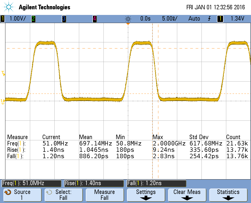
204MHz clock output on CLK0 pin measured at TP_CLK0: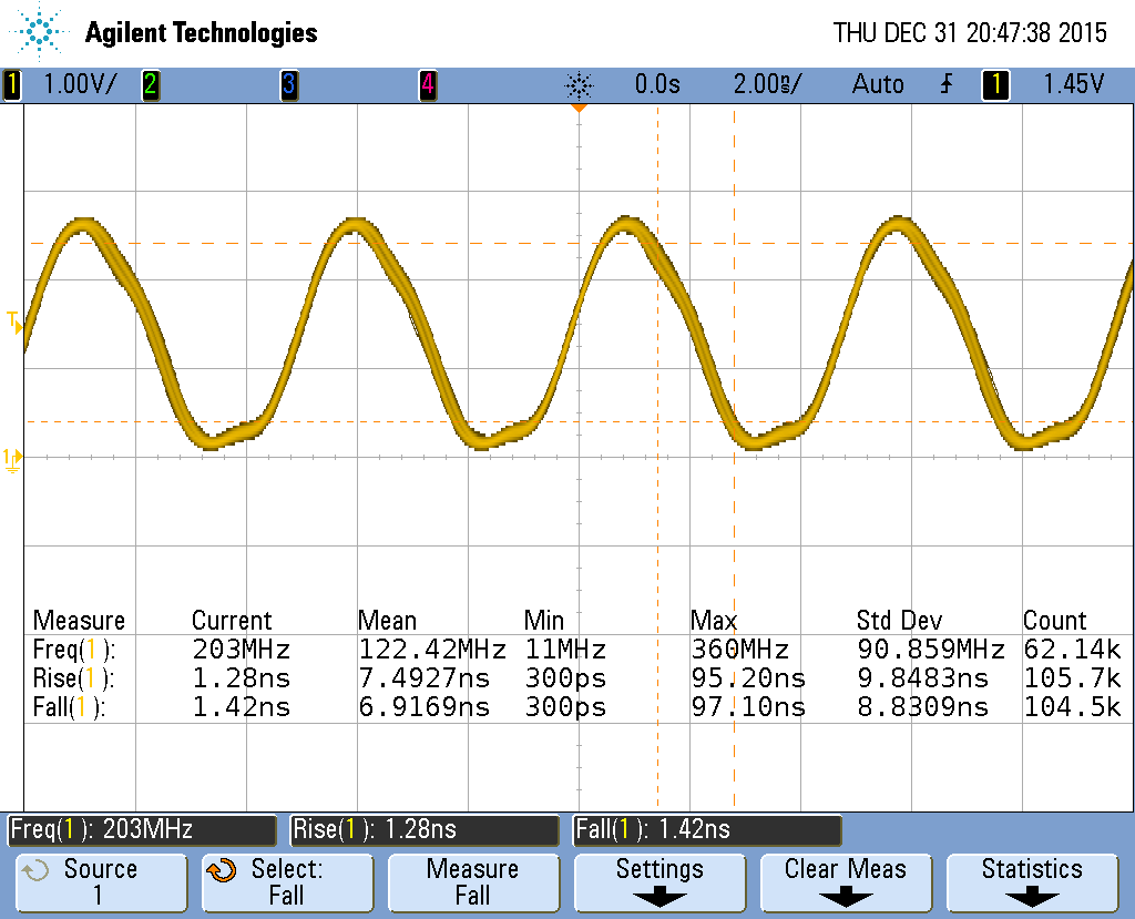
18.55MHz on pin P1_1(GPIO0[8]) measured at R45, -O0 gcc optimisation:
51MHz on pin P1_1(GPIO0[8]) measured at R45, -O3 gcc optimisation: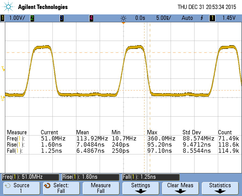
-
Nice.
-
Scope is Agilent/Keysight MSO7104B 1GHz @ 4GSa/s real time sampling.
Must be nice to have a $30K scope.
-
Scope is Agilent/Keysight MSO7104B 1GHz @ 4GSa/s real time sampling.
Must be nice to have a $30K scope.
... especially when it "only" cost $5.7k on an offer made to Keysight's eBay store (171772308652) plus a bit of liberation. N2874A 10:1 1.5GHz resistive probe was $75 on eBay (151761749582).
Here are the 204MHz and 51MHz traces with an Agilent 1130A 1.5GHz FET probe with E2676A single ended browser, 25k ohm // 0.67pF ($75 on eBay 151754375999).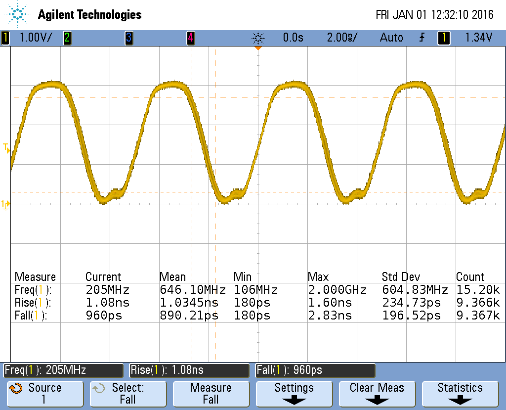
-
That's impressive GPIO switching performance at normal drive.
I wonder how low (rise and fall) can you get it if you configure the output pin to be High Speed (page 109)
http://www.nxp.com/documents/data_sheet/LPC4370.pdf
Also the price for that Link2 board looks great
http://www.findchips.com/search/OM13054
Are there any limitations on the free LPCXpresso other than been able to debug past 256K?
For example do they restrict things like using -O3?
Hmm, sorry I thought I'd posted the code in that last post. I did indeed have the high speed on on that pin.Code: [Select]#include "board.h"
#define LED0_PORT 0
#define LED0_PIN 8
int main(void)
{
LPC_GPIO_T *pGPIO=(LPC_GPIO_T *)0x400F4000;
SystemCoreClockUpdate();
Board_Init();
Chip_SCU_PinMuxSet(1,1,SCU_PINIO_FAST | SCU_MODE_FUNC0); // Setup pin for fast rise & fall time
while (1)
{
pGPIO->B[LED0_PORT][LED0_PIN] = 1;
pGPIO->B[LED0_PORT][LED0_PIN] = 0;
}
return 0;
}
Without setting fast IO, you get this: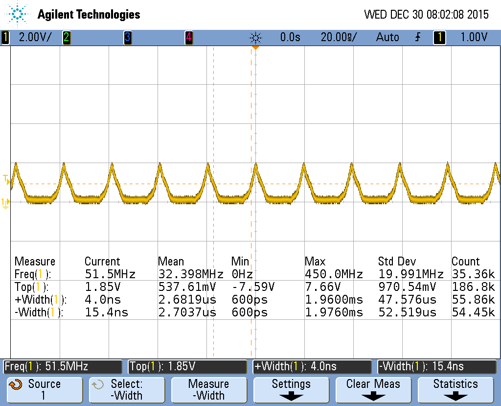
There are no restrictions on the free version other than the 256kB code limit, which is a pretty big program in this end of the embedded world.
To develop, note that there is no integrated debugger on the LPC Link2, so to get started, you actually need two, one that acts as debugger and the other that's the target. Each LPC Link2 comes with the appropriate debugging cable. The fine pitch headers are a bit of a PITA as inevitably you have to make your own breakouts, and if you wanted to integrate this board into your own product the cost of the mating connectors for a daughter board isn't cheap.


