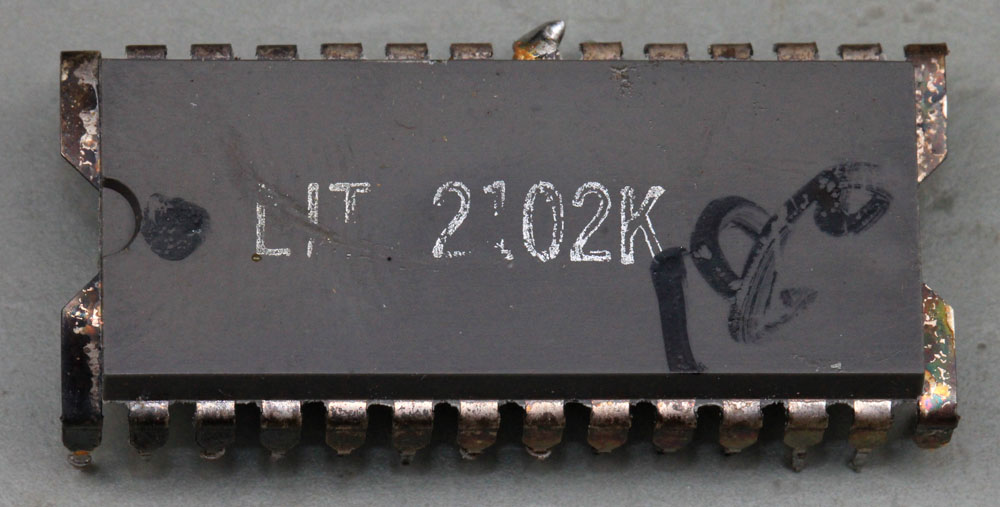
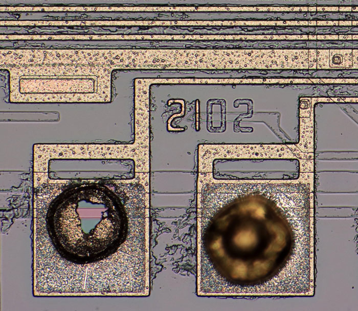
The LIT-2102 is a calculator controller manufactured by the American company Litronix. The package material resembles a gray compound that is more reminiscent of hard silicone than epoxy.
A silicone potting protects the die.
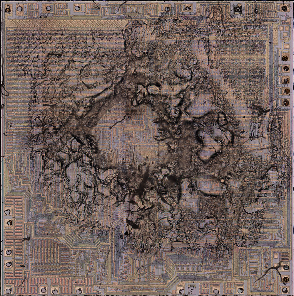
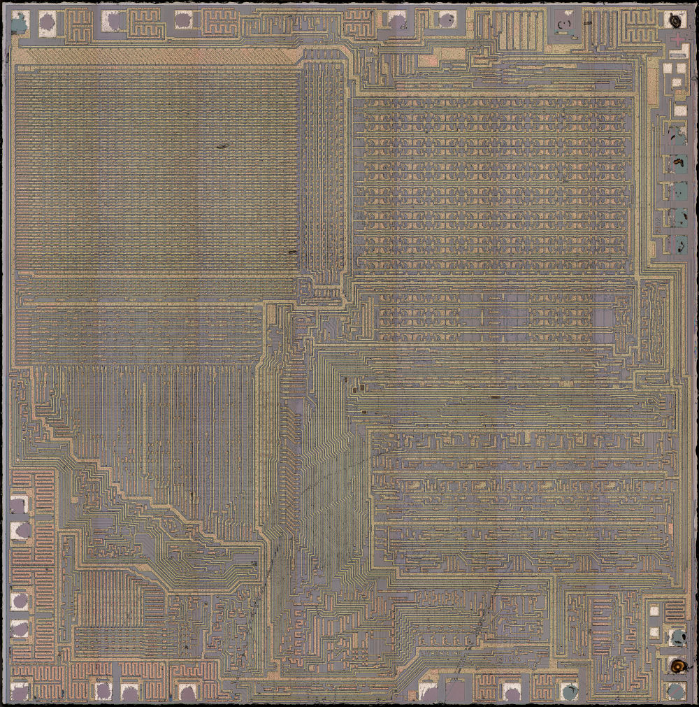
The LIT-2102 contains a die measuring 4,6mm x 4,7mm.
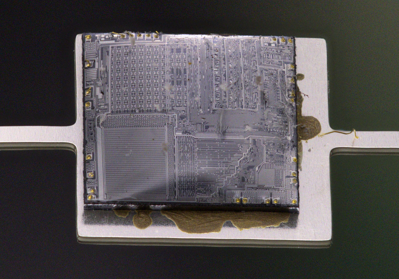
This image is also available in a higher resolution:
https://www.richis-lab.de/images/calc/23x03XL.jpg (185MB)
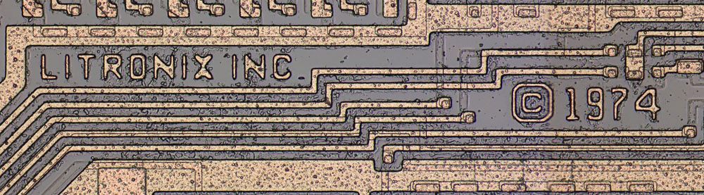
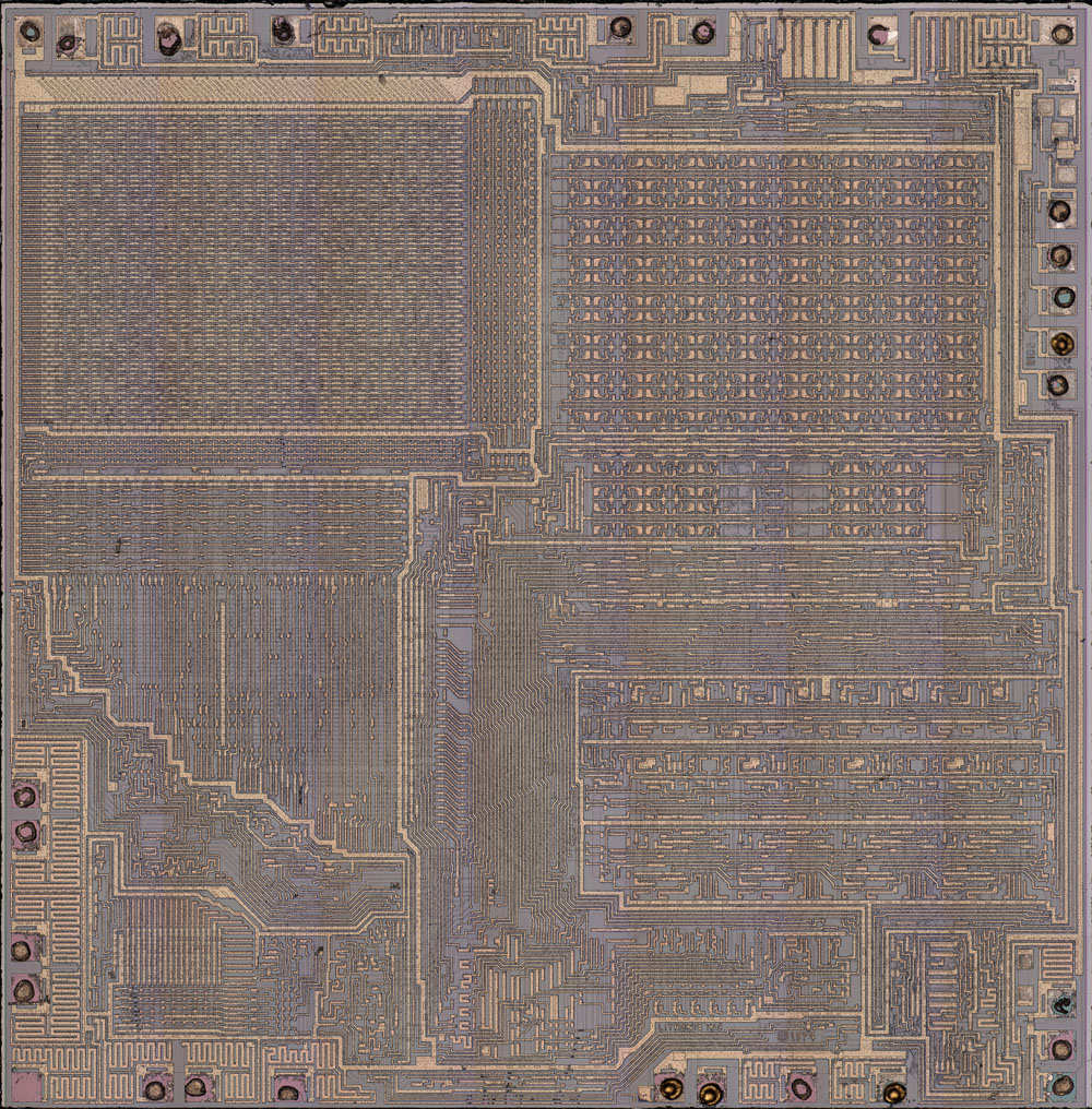
The design appears to be built by Litronix, dating back to 1974.
The number sequence 2102 and its placement in two levels suggest that there is an overarching basic design for the LIT-2100 family and that the LIT-2102 is a variant of it. The lower mask defines the different functionality. This mask determines either where contacts are formed or where a gate oxide should be located.
On the right edge, the letters “US” appear to have been placed one below the other three times. The letters are not immediately recognizable, partly because they are integrated into the circuit as functional components.
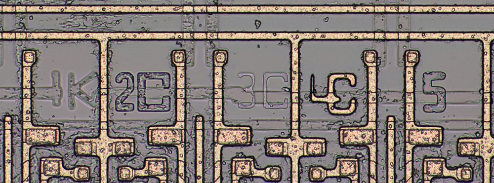
The revisions of five masks are shown to the left of the RAM area. The characters 4C have been joined together to save space.
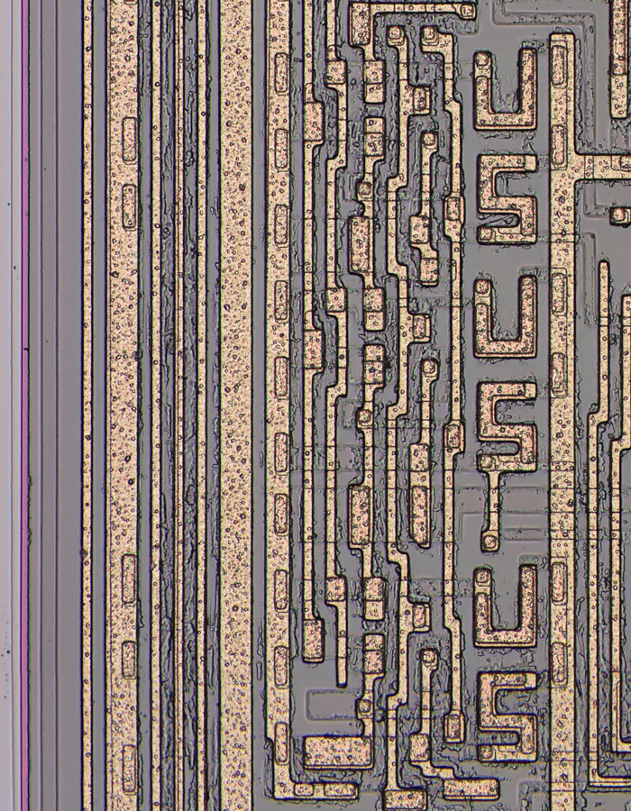
In the lower section of the die, it was clearly a struggle to route the traces.
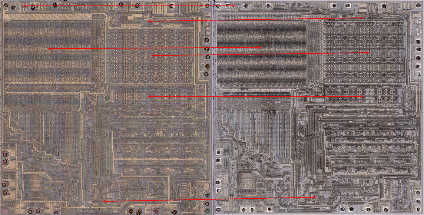
The LIT-2102 is very similar to the LIT-2314 (
https://www.richis-lab.de/calc14.htm). Upon closer inspection, however, a few differences become apparent (list is not exhaustive):
The space required for the output stages at the bond pads has been slightly reduced compared to the LIT-2314. The circuitry in the upper right area has changed significantly. In the case of the ROM (upper left), not only has the surrounding circuitry changed, but also the memory depth. The LIT-2102 has 64x64 memory cells, while the LIT-2314 operates with 96x64 memory cells. The RAM (top right) has also been modified. The memory depth differs slightly in the upper and lower sections. Circuitry components have also been changed along the lower edge.
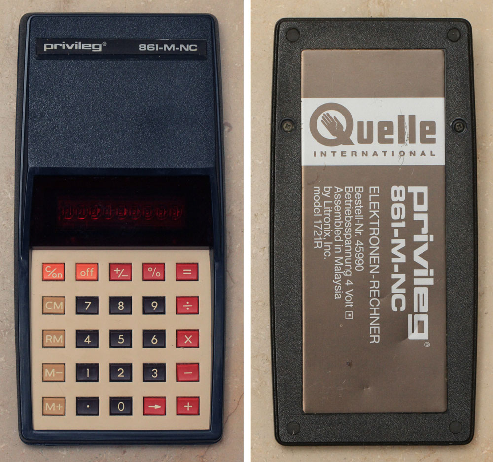
The LIT-2102 shown above was removed from the Privileg 861-M-NC calculator pictured here.
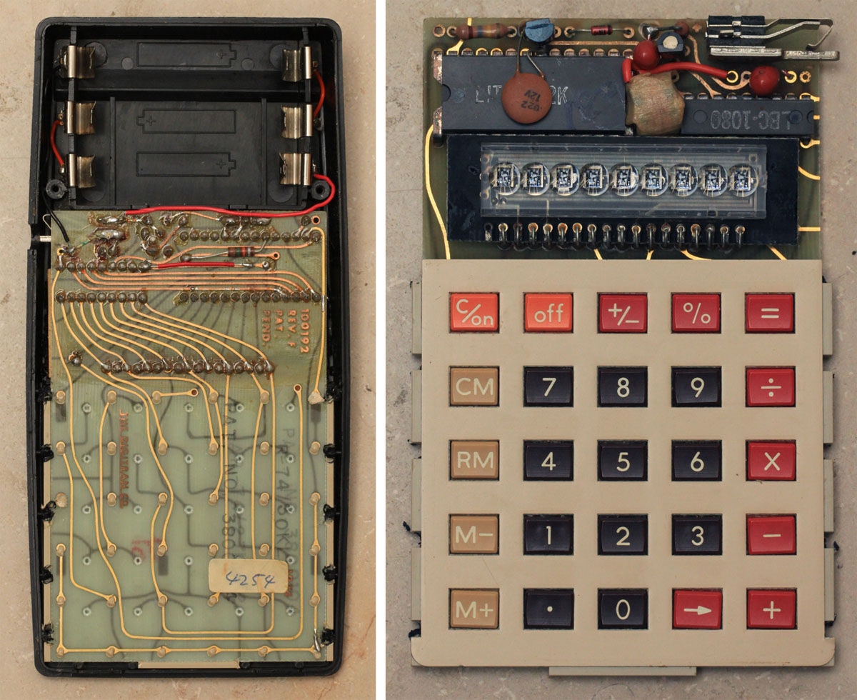
The LIT-2102 is located above the display. The LBC-1080 next to it is not just a segment driver; it is a special auxiliary component.
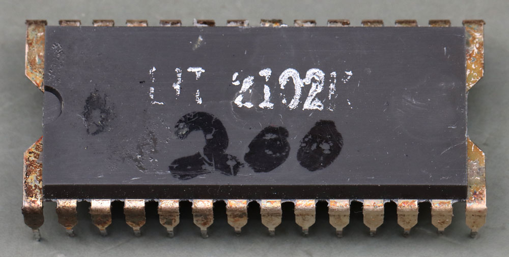
Here is a second LIT2102. Upon closer inspection, you can see an irregularity in the center of the package.
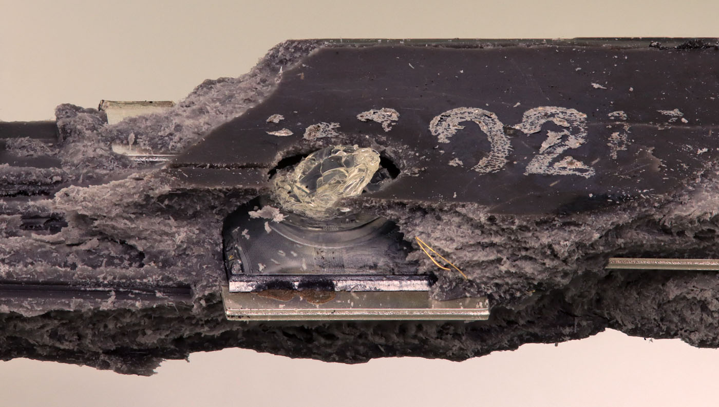
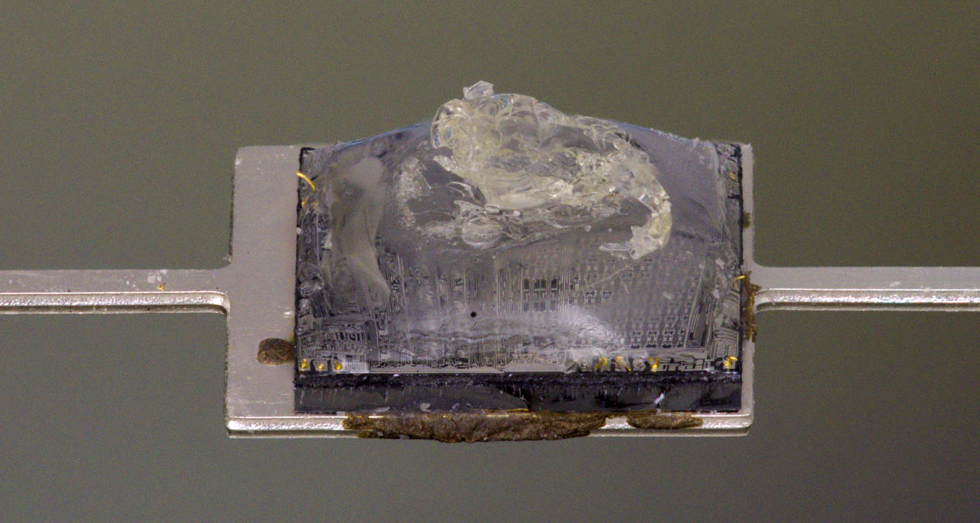
It appears that the irregularity was caused by an excessive amount of silicone. The package material was so thin at this point that it could no longer form a stable layer. From a durability standpoint, this is a major problem, as many substances can diffuse through silicone. It protects the die only from mechanical influences; the package material must provide protection against environmental influences.
Silicone is very difficult to remove without leaving any residue. So-called silicone removers only loosen the silicone; they do not dissolve it. Silicone residue between the circuit traces is particularly stubborn.
No differences can be detected between the two LIT-2102.
This image is also available in a higher resolution:
https://www.richis-lab.de/images/calc/24x05XL.jpg (117MB)
https://www.richis-lab.de/calc20.htm 


