Author Topic: Different die pictures  (Read 212205 times)

0 Members and 7 Guests are viewing this topic.

Offline RoGeorge

  • Super Contributor
  • ***
  • Posts: 8487
  • Country: ro
Re: Different die pictures
« Reply #475 on: February 18, 2026, 05:04:55 pm »
As usual, thanks for the pics.  :-+

Is this the same Omron company that does the Omron microswitches (never seen Omron ICs before  :-//).

Offline NoopyTopic starter

  • Super Contributor
  • ***
  • Posts: 2404
  • Country: de
    • Richis-Lab
Re: Different die pictures
« Reply #476 on: February 18, 2026, 05:42:20 pm »
Thanks! I'm looking forward to share a lot more pictures.  8)

As far as I know it's the same Omron.  :-+ Omron did a lot of things during the past decades.
 
The following users thanked this post: RoGeorge

Offline NoopyTopic starter

  • Super Contributor
  • ***
  • Posts: 2404
  • Country: de
    • Richis-Lab
Re: Different die pictures
« Reply #477 on: February 24, 2026, 04:03:24 am »


The BT8922H2 is a special microcontroller from the Chinese company Bluetrum, founded in 2016. The component is apparently used in in-ear headphones. A correspondingly small QFN32 package was chosen for the package (4mm x 4mm). The core of the microcontroller is a 125 MHz RISC-V processor with DSP functionalities. 256kB RAM and 16Mbit flash are available as memory.

A Bluetooth transceiver has been integrated into the BT8922H2. In addition, there is a stereo DAC, two inputs with microphone amplifiers, and two audio ADCs. The chip offers some functions typical for a microcontroller and can operate as a USB 2.0 host. It also has special functions such as wear detection and monitoring of touch buttons with low energy consumption.


The package contains a die measuring 2,0mm x 1,8mm. The RF circuits are clearly visible in the upper right-hand area. Functions such as DACs and ADCs are presumably integrated on the left edge. It is noticeable that additional bondpads are placed within the outer bond frame. These bondpads most likely connect to the flash memory, which was placed on the controller as an additional die.

This image is also available in higher resolution: https://www.richis-lab.de/images/uC/11x02XL.jpg (40MB)


The area of the RF circuits is somewhat more open and gives at least a sense of the structural sizes in the metal layers.


The 16Mbit flash memory is placed on the microcontroller as an additional die measuring 0,97mm x 1,28mm. Eight bondwires connect the two components. It is interesting to note how many different bond options the memory offers. In the lower area, some bondpad pairs appear to serve only as electrical connections between two bondwires.

This image is also available in a higher resolution: https://www.richis-lab.de/images/uC/11x05XL.jpg (53MB)


While the lower part represents the actual memory, the upper part houses the control unit. The memory comes from the Chinese company Puya. It can be assumed that PY1902V1 is an internal designation. The letter C could stand for a revision of the design.


https://www.richis-lab.de/uC11.htm

 :-/O
 
The following users thanked this post: RoGeorge, D Straney

Offline NoopyTopic starter

  • Super Contributor
  • ***
  • Posts: 2404
  • Country: de
    • Richis-Lab
Re: Different die pictures
« Reply #478 on: February 27, 2026, 04:38:49 am »


The JL7013A6 is a microcontroller in a QFN-68 package. The logo, reminiscent of the symbol Pi, belongs to the Chinese company Jieli Technology, founded in 2010. The datasheet lists typical applications as smart watches, smart speakers, and other home applications with Bluetooth interfaces.


The block diagram in the datasheet shows the integrated function blocks. The dual-core CPU operates at up to 160 MHz. The number 6 at the end of the designation indicates the version with 16MBit flash memory. PSRAM is not integrated. For this to be the case, there would need to be another number after the number 6.


The package contains a die measuring 2,2mm x 2,1mm. The RF circuit of the Bluetooth transceiver can be seen in the upper left corner. The lower right corner probably contains circuit components such as ADCs and DACs. Where the upper metal layer is used solely for power supply, the logic circuits and integrated RAM are most likely located. The flash memory, which is mounted on the microcontroller as a separate die, is connected via the partially double-row bondpads.

This image is also available in higher resolution: https://www.richis-lab.de/images/uC/12x02XL.jpg (51MB)


The dimensions of the flash memory are 1,3mm x 1,4mm. The bondpads in the center of the die appear to serve only to connect bondwires to each other. These contacts may be used if additional PSRAM needs to be connected.

This image is also available in higher resolution: https://www.richis-lab.de/images/uC/12x03XL.jpg (18MB)


The manufacturer of the memory cannot be identified. Only the character string S1224 has been integrated into the top metal layer.


https://www.richis-lab.de/uC12.htm

 :-/O
 
The following users thanked this post: RoGeorge, D Straney

Offline NoopyTopic starter

  • Super Contributor
  • ***
  • Posts: 2404
  • Country: de
    • Richis-Lab
Re: Different die pictures
« Reply #479 on: February 27, 2026, 04:39:45 am »


The JL7014F5 is very similar to the JL7013A6. The QFN-42 package is not square.


The JL7014F5 is also very similar to the JL7013A6 in terms of its block diagram. The only differences are the absence of PSRAM and the IIS digital audio interface. The suffix 5 stands for the version with 64MBit flash memory.


At first glance, it appears that the same die as in the JL7013A6 has been used.

This image is also available in a higher resolution: https://www.richis-lab.de/images/uC/13x02XL.jpg (52MB)


The dimensions of the 64MBit flash memory are 1,8mm x 2,2mm. The long edge is therefore the same length as the long edge of the microcontroller. This makes it almost impossible to place the two dies on top of each other. Perhaps this was one reason for choosing the elongated package. A clear division into four sections can be seen on the die. Each section has a whole row of double-connected bondpads.

This image is also available in a higher resolution: https://www.richis-lab.de/images/uC/13x03XL.jpg (50MB)


The memory is from Puya and has the internal designation PY1903V2. The letter A could stand for the revision of the design.


https://www.richis-lab.de/uC13.htm

 :-/O
 
The following users thanked this post: RoGeorge, D Straney

Offline NoopyTopic starter

  • Super Contributor
  • ***
  • Posts: 2404
  • Country: de
    • Richis-Lab
Re: Different die pictures
« Reply #480 on: March 04, 2026, 03:52:35 am »


And here you see what is hidden under the metal layers. Although the Flash memory is placed externaly there are a lot of memory areas on the die.

This image is also available in a higher resolution: https://www.richis-lab.de/images/uC/12x06XL.jpg (141MB)


https://www.richis-lab.de/uC12.htm#sub

 :-/O
 
The following users thanked this post: RoGeorge, iMo

Offline NoopyTopic starter

  • Super Contributor
  • ***
  • Posts: 2404
  • Country: de
    • Richis-Lab
Re: Different die pictures
« Reply #481 on: March 18, 2026, 04:25:35 am »


The TMS0803 is the successor to the TMS0102.


The die measures 5,0mm x 5,0mm.

This image is also available in a higher resolution: https://www.richis-lab.de/images/calc/15x02XL.jpg (60MB)


The numbers 0800 are printed on the metal layer, while 0803A can be seen in a lower layer. As with other Texas Instruments calculator series, the variants differ here as well on a lower layer.


There are six masks shown in the lower right corner.


The die contains several different test structures.


The TMS0803 documented here was located in a Texas Instruments TI-1500.


A leaking battery has severely damaged the circuit board of the TI-1500.


https://www.richis-lab.de/calc13.htm

 :-/O
 
The following users thanked this post: RoGeorge, D Straney

Offline NoopyTopic starter

  • Super Contributor
  • ***
  • Posts: 2404
  • Country: de
    • Richis-Lab
Re: Different die pictures
« Reply #482 on: March 21, 2026, 04:37:27 am »


The LIT-2314 is a calculator controller manufactured by the American company Litronix. The package material resembles the gray compound which is more reminiscent of hard silicone than epoxy.


LIT-2314 contains a die measuring 4,6mm x 4,7mm. Residues of the special package material remain on the surface, which cannot be removed thermally. These residues are not soluble in common solvents.

This image is also available in higher resolution: https://www.richis-lab.de/images/calc/16x02XL.jpg (63 MB)


The design was created by Litronix itself. The copyright date is 1974.


In total, there are six mask designations. The number 23 is depicted in the metal layer, with the number 14 directly next to it. It seems very likely that the sequence 2314 is related to the part name. In this case, 23 stands for the base design 2300, of which several variants exist, and the mask with the number 14 defines the specific variant.


In the center of the die, there is an additional "2" in the metal layer.


In the upper-right corner of the screen, there is an interesting test structure that allows you to measure various elements.


The documented LIT-2314 comes from the Litronix 2250 calculator shown here.


The LIT-2314 is located above the display. The LIT-1082 next to it is not just a segment driver; it is a special auxiliary circuit.


https://www.richis-lab.de/calc14.htm

 :-/O
 
The following users thanked this post: RoGeorge

Offline NoopyTopic starter

  • Super Contributor
  • ***
  • Posts: 2404
  • Country: de
    • Richis-Lab
Re: Different die pictures
« Reply #483 on: March 21, 2026, 04:38:23 am »


The Litronix LBC-1082 is a peripheral integrated circuit used in conjunction with the LIT-2314 calculator controller.


The die measures 1,7mm x 1,4mm. A slightly clearer image follows. The designation LBC1082 is visible in the lower left corner.

This image is also available in higher resolution: https://www.richis-lab.de/images/calc/17x02XL.jpg (33 MB)


The LBC-1082 has four inputs (yellow) that, via a matrix, enable the control of 9 digits (red). In the upper right section, there is an isolated circuit connected to three bondpads (green). Looking at the circuit connected to the outer pins there, it appears to be an auxiliary circuit for the calculator’s power supply. A single, larger component is also integrated along the top edge, which is not connected to any other parts of the circuit (blue). The corresponding bondpad was not used. It is likely a diode or Zener diode that could also be used in the power supply section.


Here is another LBC-1082, which bears the full designation.


This die appears to have exactly the same structure as the first die. However, it sustained less damage during the excavation.

This image is also available in a higher resolution: https://www.richis-lab.de/images/calc/18x02XL.jpg (32MB)


 :-/O
 
The following users thanked this post: RoGeorge, D Straney

Offline NoopyTopic starter

  • Super Contributor
  • ***
  • Posts: 2404
  • Country: de
    • Richis-Lab
Re: Different die pictures
« Reply #484 on: April 01, 2026, 03:16:06 am »


The Quintic QN8075 is a complete FM receiver controlled via an I2C interface. Quintic is an American company that has been acquired by NXP.


The die has an edge length of 1,2mm.

This image is also available in a higher resolution: https://www.richis-lab.de/images/radio/04x03XL.jpg (63 MB)


The left edge reveals that the QN8075 is based on the QN8035, a very similar FM receiver. The manufacturing process appears to involve six metal layers.


https://www.richis-lab.de/radio04.htm

 :-/O
 
The following users thanked this post: RoGeorge, D Straney

Online Renate

  • Super Contributor
  • ***
  • Posts: 1749
  • Country: de
    • Renate's Android Page
Re: Different die pictures
« Reply #485 on: April 01, 2026, 07:55:56 am »
Is that an antenna in the lower right corner of the QN8075?
 

Offline NoopyTopic starter

  • Super Contributor
  • ***
  • Posts: 2404
  • Country: de
    • Richis-Lab
Re: Different die pictures
« Reply #486 on: April 01, 2026, 10:35:24 am »
No, that is just an inductance. Something in the RF part, could be the oscillator.  :-//

Offline NoopyTopic starter

  • Super Contributor
  • ***
  • Posts: 2404
  • Country: de
    • Richis-Lab
Re: Different die pictures
« Reply #487 on: April 14, 2026, 03:07:55 am »


The TMS0102 calculator controller had three successors: the TMS0600, TMS0700, and TMS0800. Each of these controllers was available in different versions. Pictured here is the TMS0601.


The die measures 5,3mm x 5,6mm.

This image is also available in a higher resolution: https://www.richis-lab.de/images/calc/19x02XL.jpg (69 MB)


There are six masks depicted in the lower left corner.


In the metal layer, the number sequence 0600 refers to the controller family. The “A” could stand for a revision. As with the other calculator controllers in this group, a lower layer appears to define the variant. The numbers 0601 are shown there.


https://www.richis-lab.de/calc16.htm

 :-/O
 
The following users thanked this post: RoGeorge, D Straney

Offline NoopyTopic starter

  • Super Contributor
  • ***
  • Posts: 2404
  • Country: de
    • Richis-Lab
Re: Different die pictures
« Reply #488 on: April 22, 2026, 09:50:05 am »


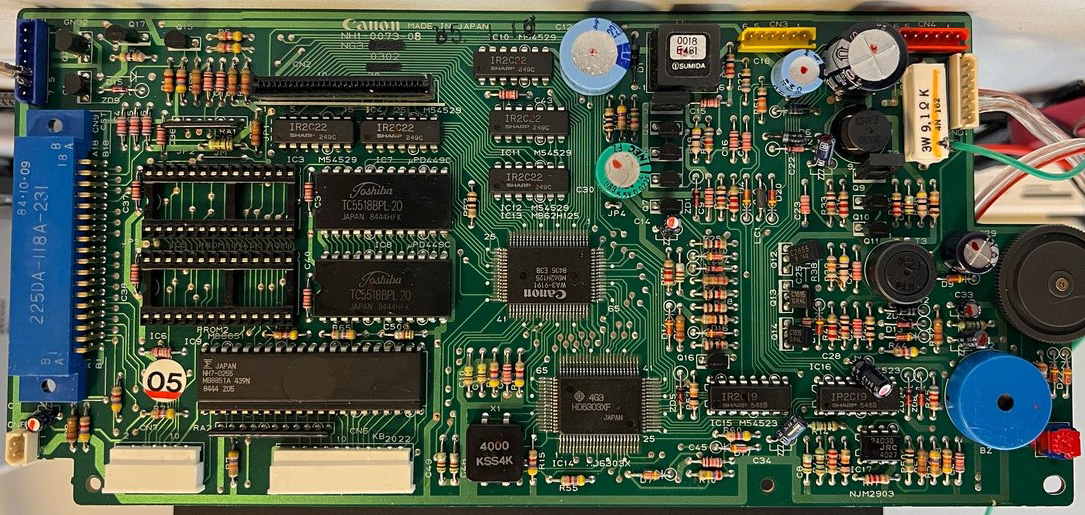
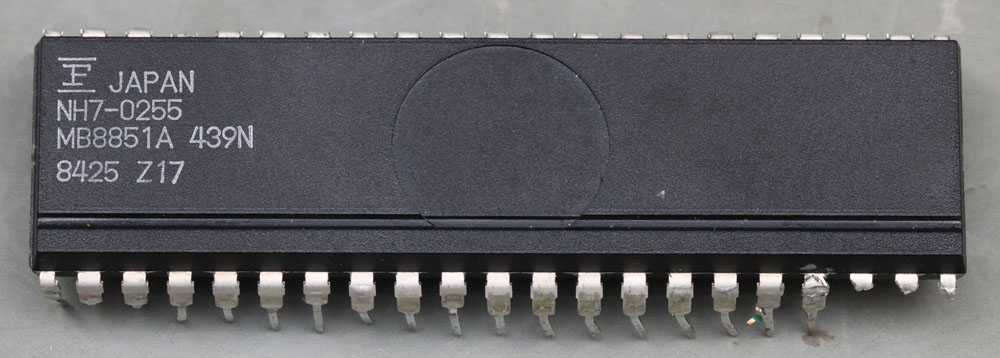
The circuit board shown above is from the Canon S-60 typewriter. The typewriter is controlled by a Hitachi HD6303XF. The additional 4Bit Fujitsu MB8851 microcontroller is used to read the keyboard matrix and cache it as needed. The pressed keys are ultimately transmitted to the main controller via a serial interface.
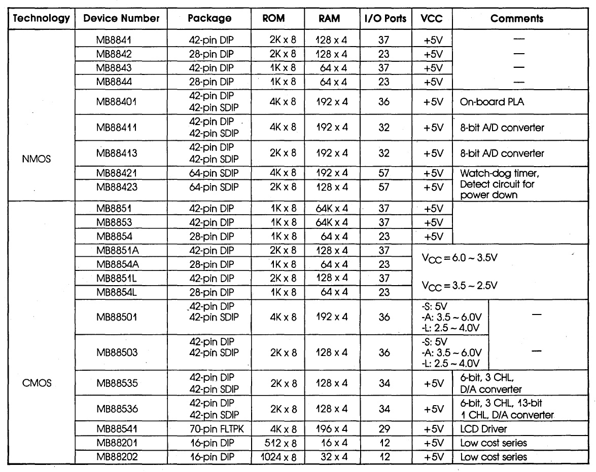


The MB8851 belongs to a whole family of microcontrollers. The MB8851 is a CMOS device that contains 2KB of ROM and 64B of RAM. The program memory is a mask ROM, meaning it is programmed during the manufacturing process.

In addition to the A variant documented here, there is a standard variant and an L variant. They differ in their permissible supply voltage and operating temperature ranges and also regarding the integrated memory.
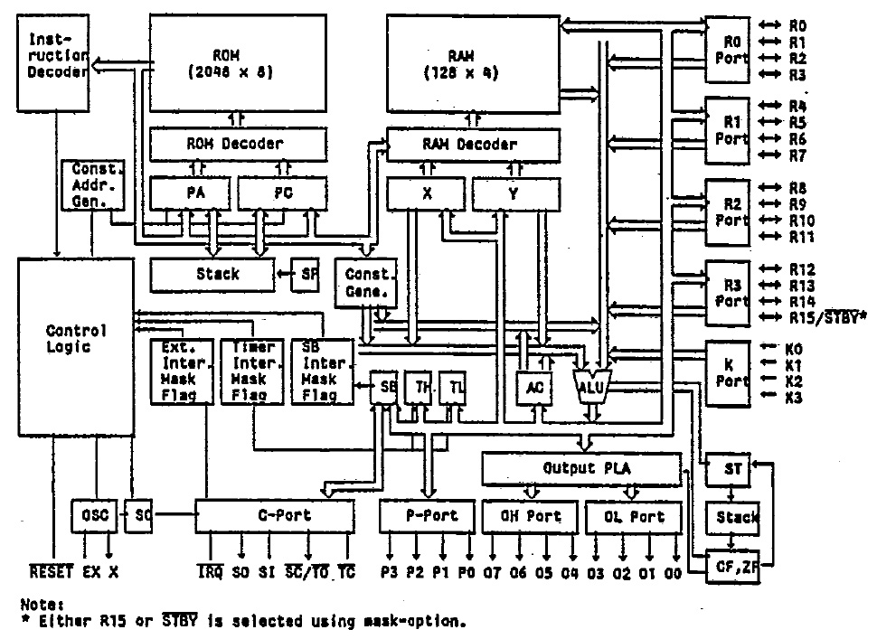


The datasheet shows the typical block diagram of a simple microcontroller. Output R15 can be reconfigured as a standby interface via the mask. The datasheet describes additional configuration options of this kind. Of particular technical interest is the programmable logic array, which enables more efficient control of Port O.
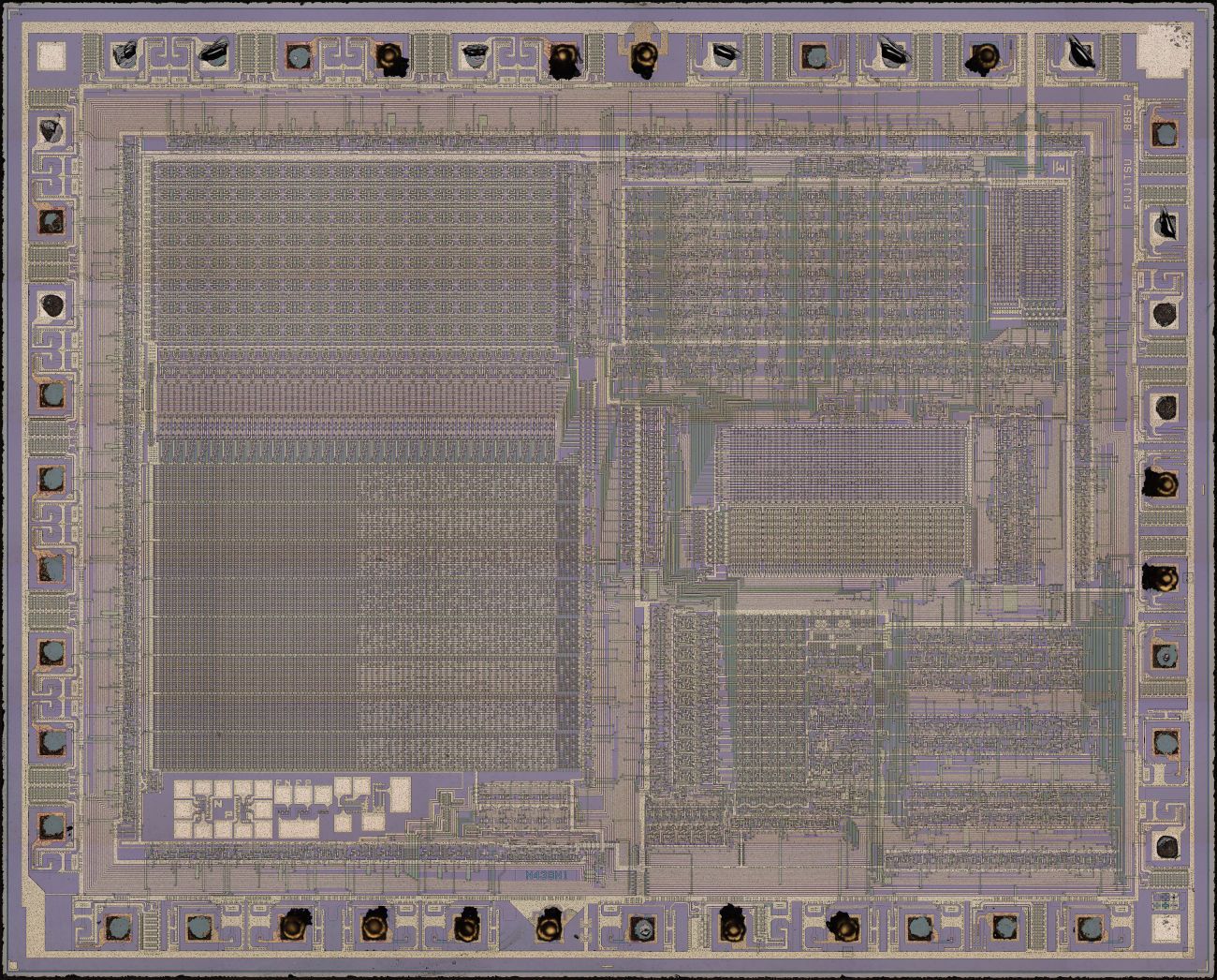


The die measures 5,7mm x 4,6mm.

This image is also available in a higher resolution: https://www.richis-lab.de/images/uC/14x05XL.jpg (220MB)
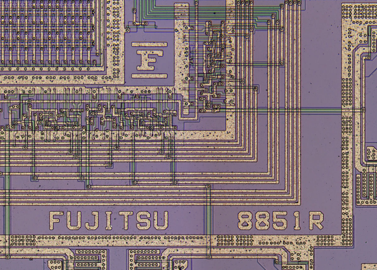


The numbers 8851 almost certainly refer to the variant of the microcontroller family. The letter R could represent a revision number.
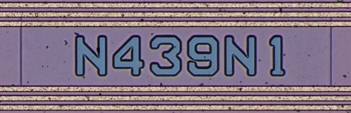


The string N439N1 could be the specific project name. As will become clear shortly, the microcontroller is programmed by putting contacts into the memory area. The mask shown here in blue could be this contact mask.
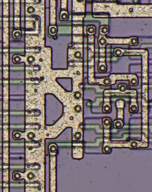


The traces on the MB8851 are efficiently laid out, as one would expect from an integrated circuit. In one spot, however, two traces are connected via a strangely intricate pattern of lines. Upon closer inspection, this might be a small, inconspicuous work of art created by the developers. It could be intertwined initials or a Japanese character.
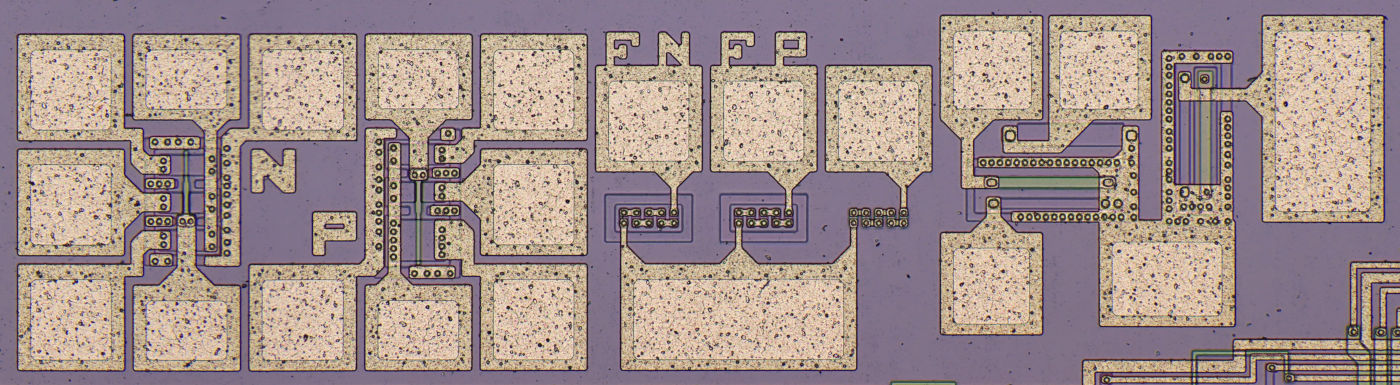


The lower left section shows several test structures. From left to right, the first structures shown are N-channel and P-channel MOSFETs of various widths. These are followed by three contact chains in different areas. At the end, you can measure strips in different areas.
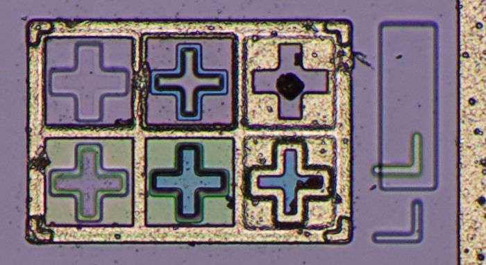


In the lower-right corner are test patterns that allow you to check the alignment of the masks relative to one another.
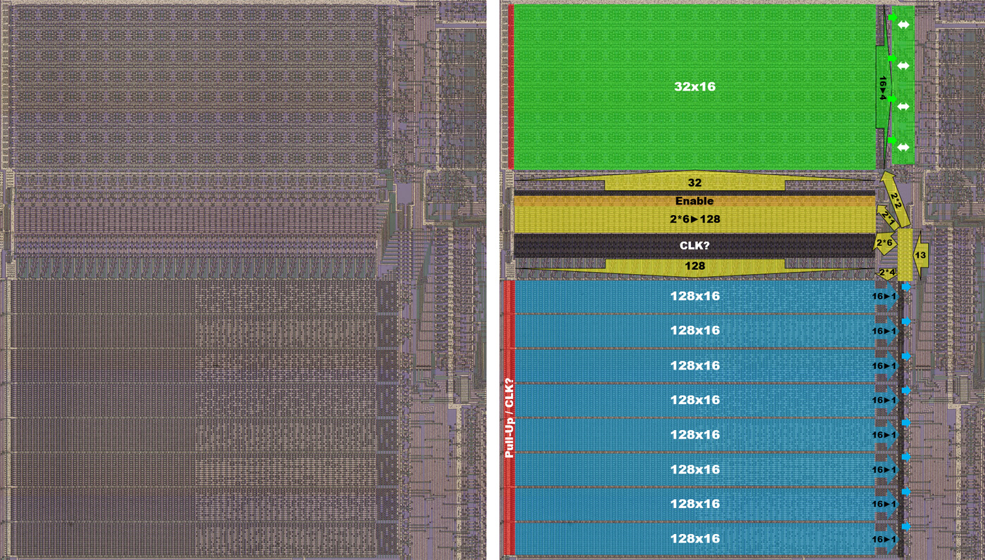


The very large memory areas occupy nearly half of the silicon. The mask ROM (blue) is located in the lower section. It is clearly visible that only half of the memory area has been used. The ROM consists of eight blocks, each with 128 columns and 16 rows. A switched pull-up structure (red) is located at the left edge. Control is not performed using a dedicated control signal. It could be a clock signal that cyclically activates the ROM. To read out an 8Bit data word, one column is activated. At the right end of the blocks, each of the eight multiplexers put out one of the rows.

Control is handled via 13 lines arriving from the right (yellow). A small circuit additionally generates the inverted control signals. Two times four control signals lead to the eight output multiplexers of the ROM. Two times six control signals lead to the area between RAM and ROM and implement the selection of one of the 128 columns. This column selection applies equally to RAM and ROM. On the ROM side, there is an additional connection with a control signal that is not exclusively assigned to the ROM (black). On the upper side, one of the control signals can activate or deactivate the selection of the RAM column.

The RAM area consists of 32 columns and 16 rows. Consequently, fewer control signals are required for column selection. Four addresses are combined for each column. Switchable pull-up structures are also located to the left of the RAM area. On the right edge, two times two control signals control four multiplexers, which ensure that a 4Bit wide word is formed from the 16 rows. This is followed by four blocks that control read and write.
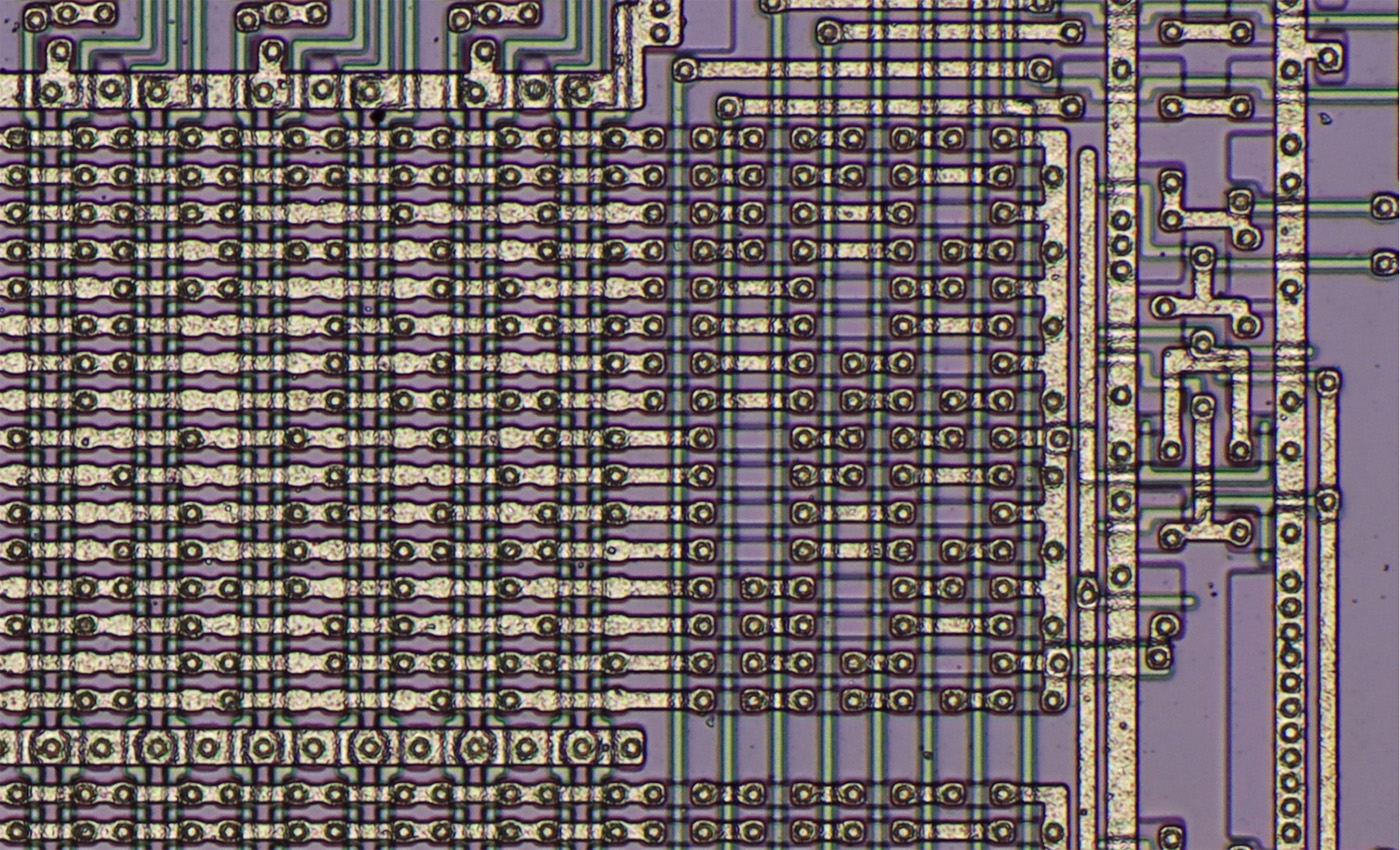
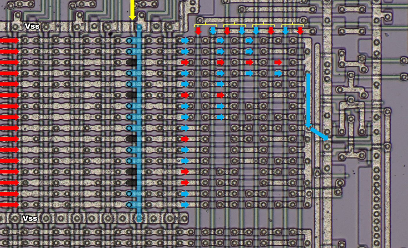


The working principle of the ROM is easy to understand. Each row is pulled to a high potential via the pull-up structure on the left edge. Column selection is performed via polysilicon strips, which serve as the gate electrodes of MOSFETs in each row. These MOSFETs are connected to the VSS potential on one side. The other side is either open or connected via a contact to the overlying metal strip. If there is a connection to the row in the active column, the potential of that row is pulled to a low level. This results in a sequence of high and low levels that depend on the placement of the contacts and thus output the programming.

The multiplexer is also very straightforward. Four control signals and their inverted signals are connected to eight polysilicon strips. The polysilicon strips form MOSFETs with transverse strips in the substrate. In some cases, short metal strips act as bridges. This results in only one row ultimately being switched through to the output.
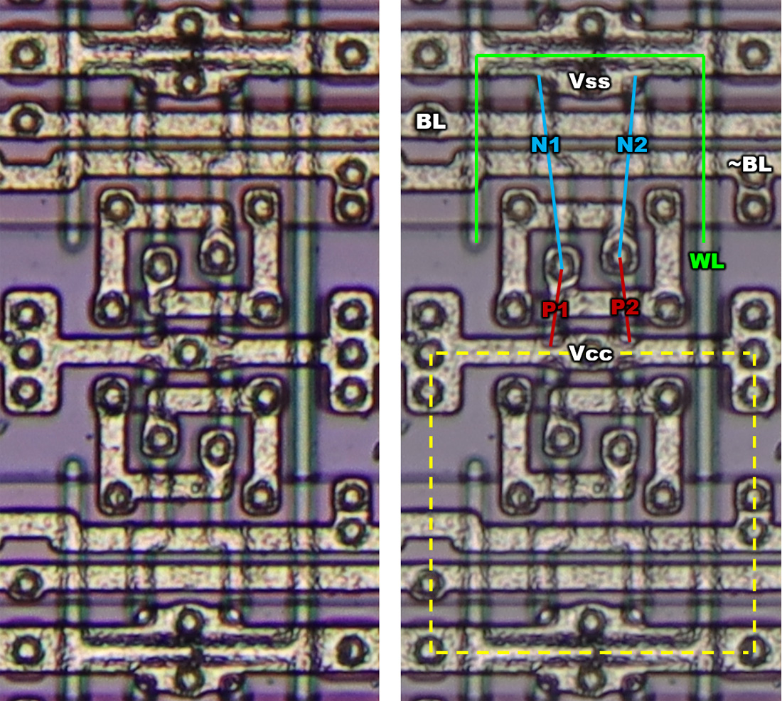


The SRAM cells consist of six transistors. Vertical word lines activate one of the columns (green). The cell can be written to and read from via the horizontal lines BL and ~BL. The memory cell itself consists of the familiar cross-connected combination of two NMOS and two PMOS transistors.
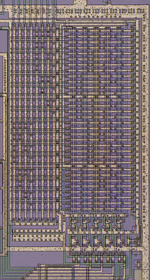


In the upper-right section of the die is the programmable logic array, which can be used to efficiently utilize Port O. The datasheet lists the control of 7-segment displays as a typical application.


https://www.richis-lab.de/uC14.htm

 :-/O
« Last Edit: April 22, 2026, 10:16:43 am by Noopy »
 
The following users thanked this post: RoGeorge, D Straney, MT4S301

Offline NoopyTopic starter

  • Super Contributor
  • ***
  • Posts: 2404
  • Country: de
    • Richis-Lab
Re: Different die pictures
« Reply #489 on: April 30, 2026, 03:42:59 am »


The Injoinic Technology IP5306 is an IC that is used in power banks to controls battery charging and the output of a stable 5V. The charging current can reach up to 2,1A. The 5V output can handle a load of up to 2,4A.


The datasheet includes a schematic diagram of a typical application. The SO-8 chip requires only a few additional passive components. The switching frequency is 750kHz during charging and 500kHz during discharging. It remains unclear why different switching frequencies were chosen. Up to four LEDs indicate the current charge status. Additionally, a flashlight function can be implemented.


The die measures 1,85mm x 1,35mm. A large logic block is located in the upper left corner. The power semiconductors are situated in the right-hand section. The power semiconductors’ terminals are connected to the outside via several bond wires. However, there still appear to be too many bond wires for the package’s eight pins.

This image is also available in a higher resolution: https://www.richis-lab.de/images/li/05x03XL.jpg (26MB)


The top metal layer has significantly coarser structures than the lower layers. It cannot be made finer because it is significantly thicker. This results in a low-impedance plane, which is very beneficial for the power section.


https://www.richis-lab.de/li05.htm

 :-/O
« Last Edit: April 30, 2026, 04:27:35 pm by Noopy »
 
The following users thanked this post: RoGeorge, D Straney

Offline magic

  • Super Contributor
  • ***
  • Posts: 8063
  • Country: pl
Re: Different die pictures
« Reply #490 on: April 30, 2026, 04:23:57 pm »
This image is also available in a higher resolution: https://www.richis-lab.de/images/li/05x03XL.jpg (26MB)
Actually, you have embedded the 26MB version already :scared:
 

Offline NoopyTopic starter

  • Super Contributor
  • ***
  • Posts: 2404
  • Country: de
    • Richis-Lab
Re: Different die pictures
« Reply #491 on: April 30, 2026, 04:28:25 pm »
This image is also available in a higher resolution: https://www.richis-lab.de/images/li/05x03XL.jpg (26MB)
Actually, you have embedded the 26MB version already :scared:

Oh... Good for everybody with big screens. ;D
Changed it...

Offline NoopyTopic starter

  • Super Contributor
  • ***
  • Posts: 2404
  • Country: de
    • Richis-Lab
Re: Different die pictures
« Reply #492 on: May 02, 2026, 04:00:35 am »


The TMS0602 is a calculator controller from the TMS0600 family.


The die dimensions are 5,85mm × 5,86mm. Surprisingly, the layout differs significantly from that of the TMS0601 (https://www.richis-lab.de/calc16.htm). While the arrangement of the major functional blocks is the same or at least very similar, this is clearly not just a variant in which only one mask has been changed.

This image is also available in higher resolution: https://www.richis-lab.de/images/calc/20x02XL.jpg (90MB)


Six masks are depicted along the bottom edge. It remains unclear whether the “A” next to mask 3 indicates a mask revision or whether it refers to a modified process step compared to TMS0601.


As with the TMS0601, the number sequence 0600 is printed on the metal layer, indicating the controller family. Below that are the numbers 0602, which identify this specific model.


https://www.richis-lab.de/calc17.htm

 :-/O
 
The following users thanked this post: RoGeorge, D Straney

Offline Ranayna

  • Super Contributor
  • ***
  • Posts: 1308
  • Country: de
Re: Different die pictures
« Reply #493 on: May 02, 2026, 11:30:47 am »
Looking at these old ICs, i find it surprising that they use all their precision making the dies, and then do such a slipshod print on the package that it does not look like they even tried to print the label straight. :D
 

Offline NoopyTopic starter

  • Super Contributor
  • ***
  • Posts: 2404
  • Country: de
    • Richis-Lab
Re: Different die pictures
« Reply #494 on: May 03, 2026, 07:12:55 pm »
I agree with you. The marking was definitely not important for them.  ;D

Offline NoopyTopic starter

  • Super Contributor
  • ***
  • Posts: 2404
  • Country: de
    • Richis-Lab
Re: Different die pictures
« Reply #495 on: May 14, 2026, 03:52:38 am »


The controller documented here comes from an Adler 80C calculator. The logo belongs to the American company Electronic Arrays. The part number is EA7044. 7432 is definitely the datecode.


The die measures 3,8mm x 3,7mm.

This image is also available in a higher resolution: https://www.richis-lab.de/images/calc/21x02XL.jpg (130MB)


The label on the bottom edge indicates that the integrated circuit was developed by Antex. According to Wikipedia, both Antex Industries and Electronic Arrays are among the so-called “Fairchildren”—that is, companies founded by former Fairchild employees. The internal designation was apparently ML1003A.


There are four masks depicted along the top edge.


Here is the calculator from which the EA7044 was taken.


https://www.richis-lab.de/calc18.htm

 :-/O
 
The following users thanked this post: RoGeorge, ch_scr, D Straney

Offline NoopyTopic starter

  • Super Contributor
  • ***
  • Posts: 2404
  • Country: de
    • Richis-Lab
Re: Different die pictures
« Reply #496 on: May 14, 2026, 03:53:26 am »


The controller documented here comes from a Litronix calculator. It appears to be designated LIT-3003, even though only the numbers 3003 are shown on the package.


A layer remains on the die that cannot be removed. At least some of the structure is still visible.

This image is also available in a higher resolution: https://www.richis-lab.de/images/calc/22x02XL.jpg (57MB)


The label visible on the bottom edge reveals that this is an Antex ML1003A, the same model used in the Electronic Arrays EA7044. This makes sense when you consider that Antex was acquired by Litronix in 1975, as documented here, for example: https://archive.computerhistory.org/resources/access/text/2016/12/102762574-05-01-acc.pdf


https://www.richis-lab.de/calc19.htm

 :-/O
 
The following users thanked this post: RoGeorge, ch_scr, AnalogTodd

Offline AnalogTodd

  • Regular Contributor
  • *
  • Posts: 221
  • Country: us
Re: Different die pictures
« Reply #497 on: May 14, 2026, 01:03:19 pm »
I'm waiting for the day I see pictures of one of my parts posted by you!
Lived in the home of the gurus for many years.
 

Offline NoopyTopic starter

  • Super Contributor
  • ***
  • Posts: 2404
  • Country: de
    • Richis-Lab
Re: Different die pictures
« Reply #498 on: May 14, 2026, 01:06:46 pm »
I still have quite a lot of parts here. We will see...  ;D

Offline Zoli

  • Frequent Contributor
  • **
  • Posts: 799
  • Country: ca
  • Grumpy old men
Re: Different die pictures
« Reply #499 on: May 15, 2026, 06:39:46 am »
That means I was lucky to wait only one year? >:D :-DD


Share me

Digg  Facebook  SlashDot  Delicious  Technorati  Twitter  Google  Yahoo
Smf


-->