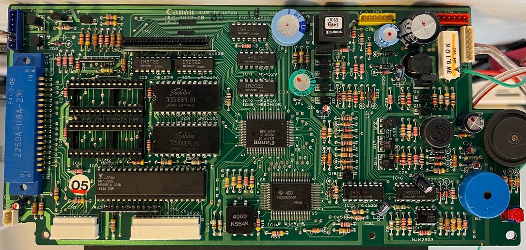
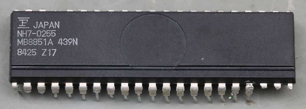
The circuit board shown above is from the Canon S-60 typewriter. The typewriter is controlled by a Hitachi HD6303XF. The additional 4Bit Fujitsu MB8851 microcontroller is used to read the keyboard matrix and cache it as needed. The pressed keys are ultimately transmitted to the main controller via a serial interface.
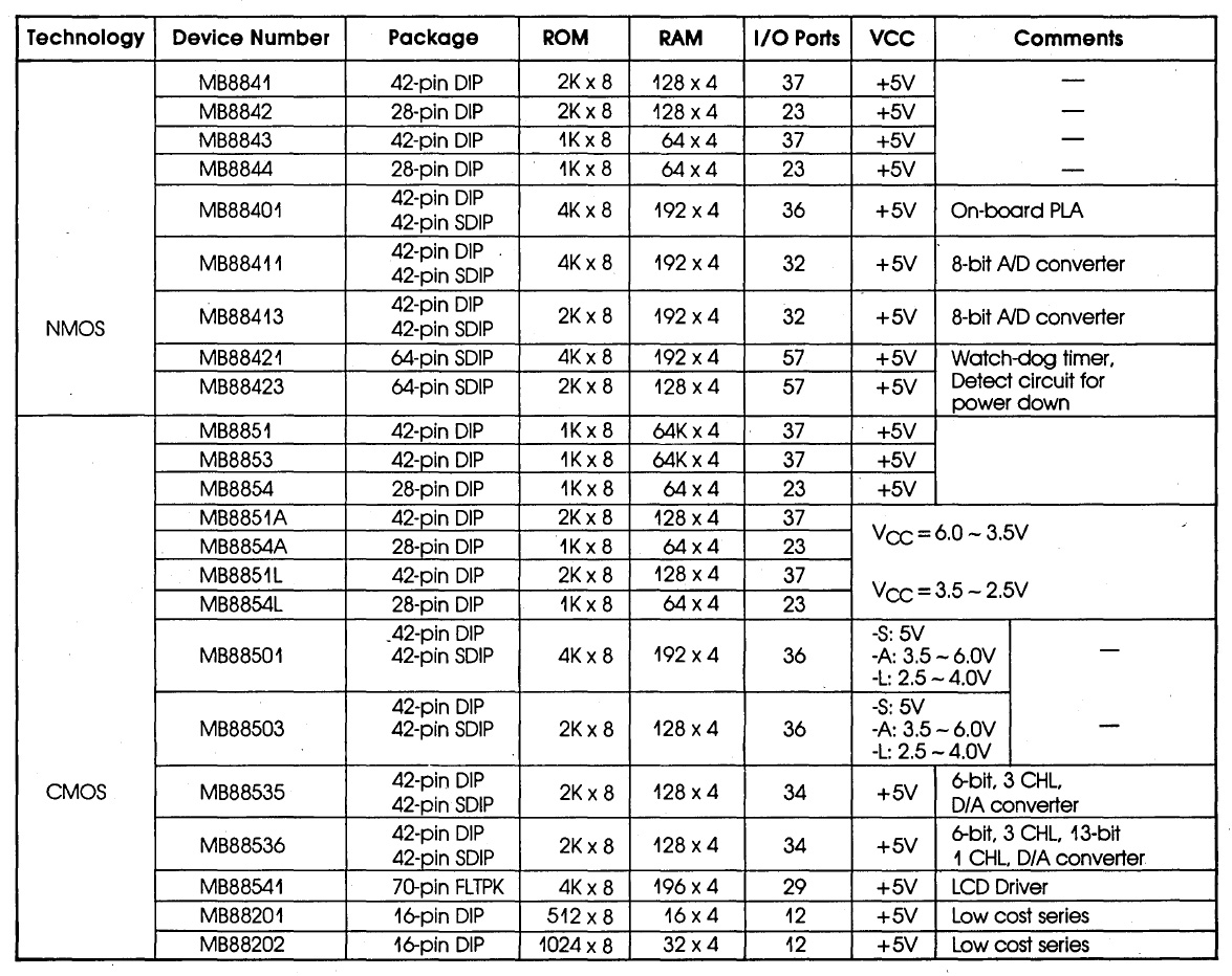
The MB8851 belongs to a whole family of microcontrollers. The MB8851 is a CMOS device that contains 2KB of ROM and 64B of RAM. The program memory is a mask ROM, meaning it is programmed during the manufacturing process.
In addition to the A variant documented here, there is a standard variant and an L variant. They differ in their permissible supply voltage and operating temperature ranges and also regarding the integrated memory.
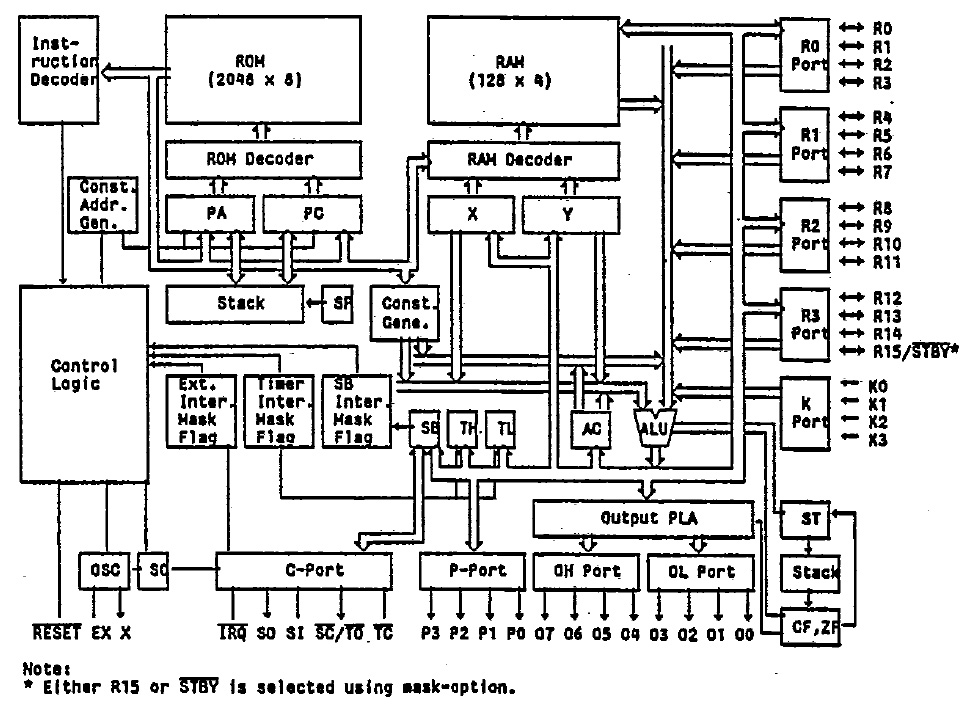
The datasheet shows the typical block diagram of a simple microcontroller. Output R15 can be reconfigured as a standby interface via the mask. The datasheet describes additional configuration options of this kind. Of particular technical interest is the programmable logic array, which enables more efficient control of Port O.
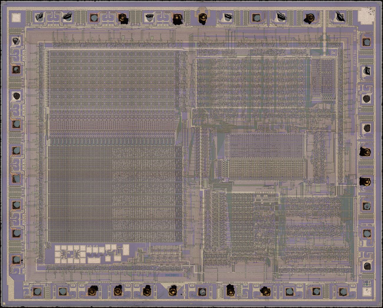
The die measures 5,7mm x 4,6mm.
This image is also available in a higher resolution:
https://www.richis-lab.de/images/uC/14x05XL.jpg (220MB)
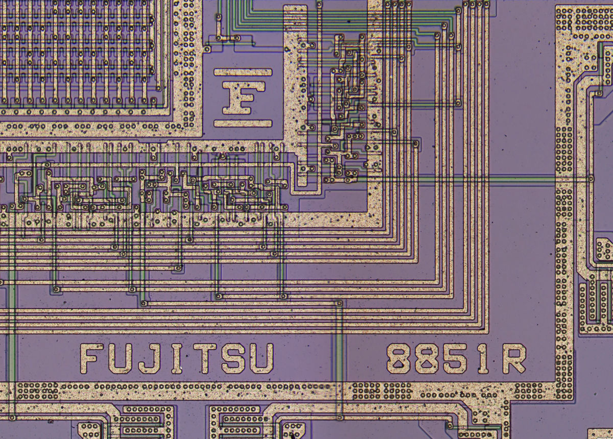
The numbers 8851 almost certainly refer to the variant of the microcontroller family. The letter R could represent a revision number.
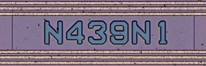
The string N439N1 could be the specific project name. As will become clear shortly, the microcontroller is programmed by putting contacts into the memory area. The mask shown here in blue could be this contact mask.
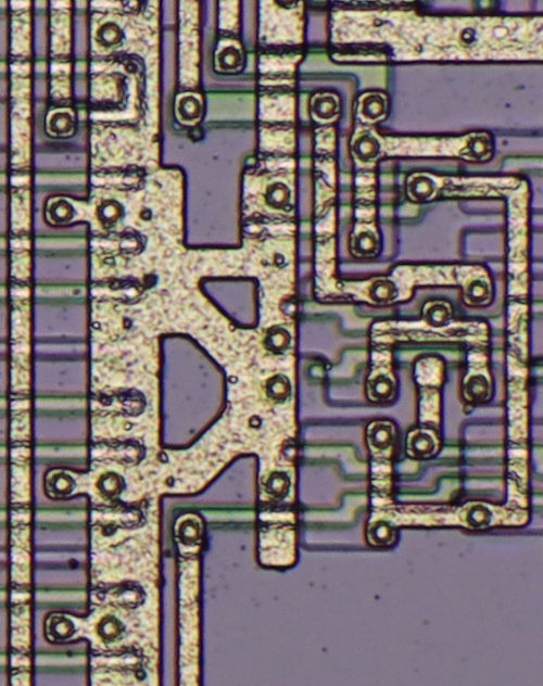
The traces on the MB8851 are efficiently laid out, as one would expect from an integrated circuit. In one spot, however, two traces are connected via a strangely intricate pattern of lines. Upon closer inspection, this might be a small, inconspicuous work of art created by the developers. It could be intertwined initials or a Japanese character.
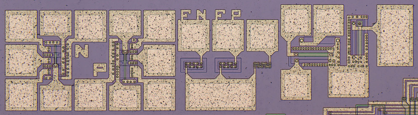
The lower left section shows several test structures. From left to right, the first structures shown are N-channel and P-channel MOSFETs of various widths. These are followed by three contact chains in different areas. At the end, you can measure strips in different areas.
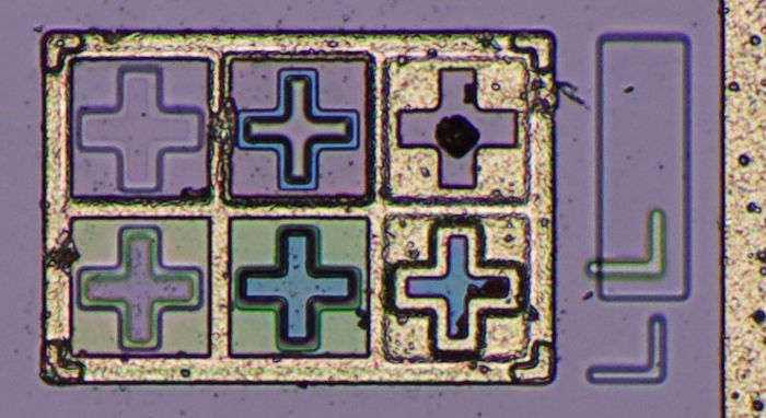
In the lower-right corner are test patterns that allow you to check the alignment of the masks relative to one another.
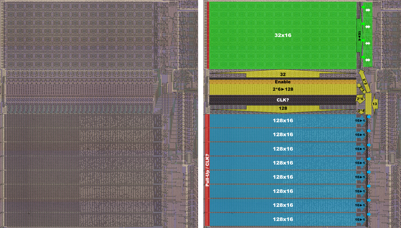
The very large memory areas occupy nearly half of the silicon. The mask ROM (blue) is located in the lower section. It is clearly visible that only half of the memory area has been used. The ROM consists of eight blocks, each with 128 columns and 16 rows. A switched pull-up structure (red) is located at the left edge. Control is not performed using a dedicated control signal. It could be a clock signal that cyclically activates the ROM. To read out an 8Bit data word, one column is activated. At the right end of the blocks, each of the eight multiplexers put out one of the rows.
Control is handled via 13 lines arriving from the right (yellow). A small circuit additionally generates the inverted control signals. Two times four control signals lead to the eight output multiplexers of the ROM. Two times six control signals lead to the area between RAM and ROM and implement the selection of one of the 128 columns. This column selection applies equally to RAM and ROM. On the ROM side, there is an additional connection with a control signal that is not exclusively assigned to the ROM (black). On the upper side, one of the control signals can activate or deactivate the selection of the RAM column.
The RAM area consists of 32 columns and 16 rows. Consequently, fewer control signals are required for column selection. Four addresses are combined for each column. Switchable pull-up structures are also located to the left of the RAM area. On the right edge, two times two control signals control four multiplexers, which ensure that a 4Bit wide word is formed from the 16 rows. This is followed by four blocks that control read and write.
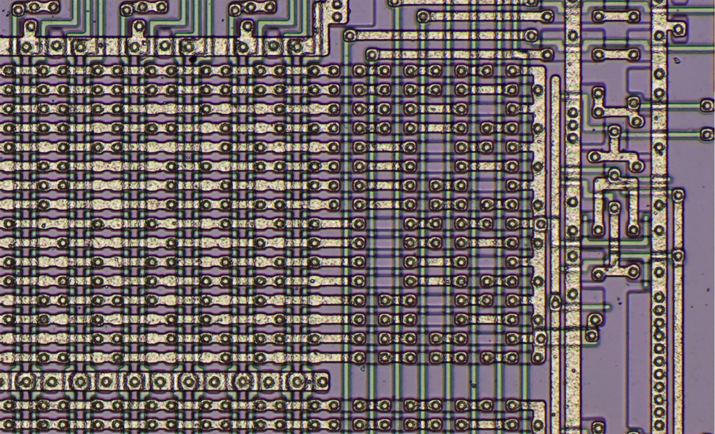
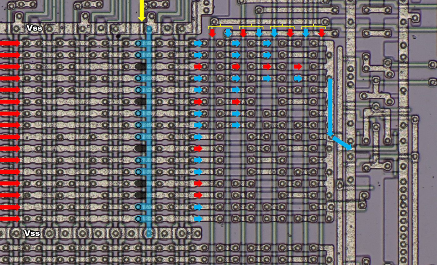
The working principle of the ROM is easy to understand. Each row is pulled to a high potential via the pull-up structure on the left edge. Column selection is performed via polysilicon strips, which serve as the gate electrodes of MOSFETs in each row. These MOSFETs are connected to the VSS potential on one side. The other side is either open or connected via a contact to the overlying metal strip. If there is a connection to the row in the active column, the potential of that row is pulled to a low level. This results in a sequence of high and low levels that depend on the placement of the contacts and thus output the programming.
The multiplexer is also very straightforward. Four control signals and their inverted signals are connected to eight polysilicon strips. The polysilicon strips form MOSFETs with transverse strips in the substrate. In some cases, short metal strips act as bridges. This results in only one row ultimately being switched through to the output.
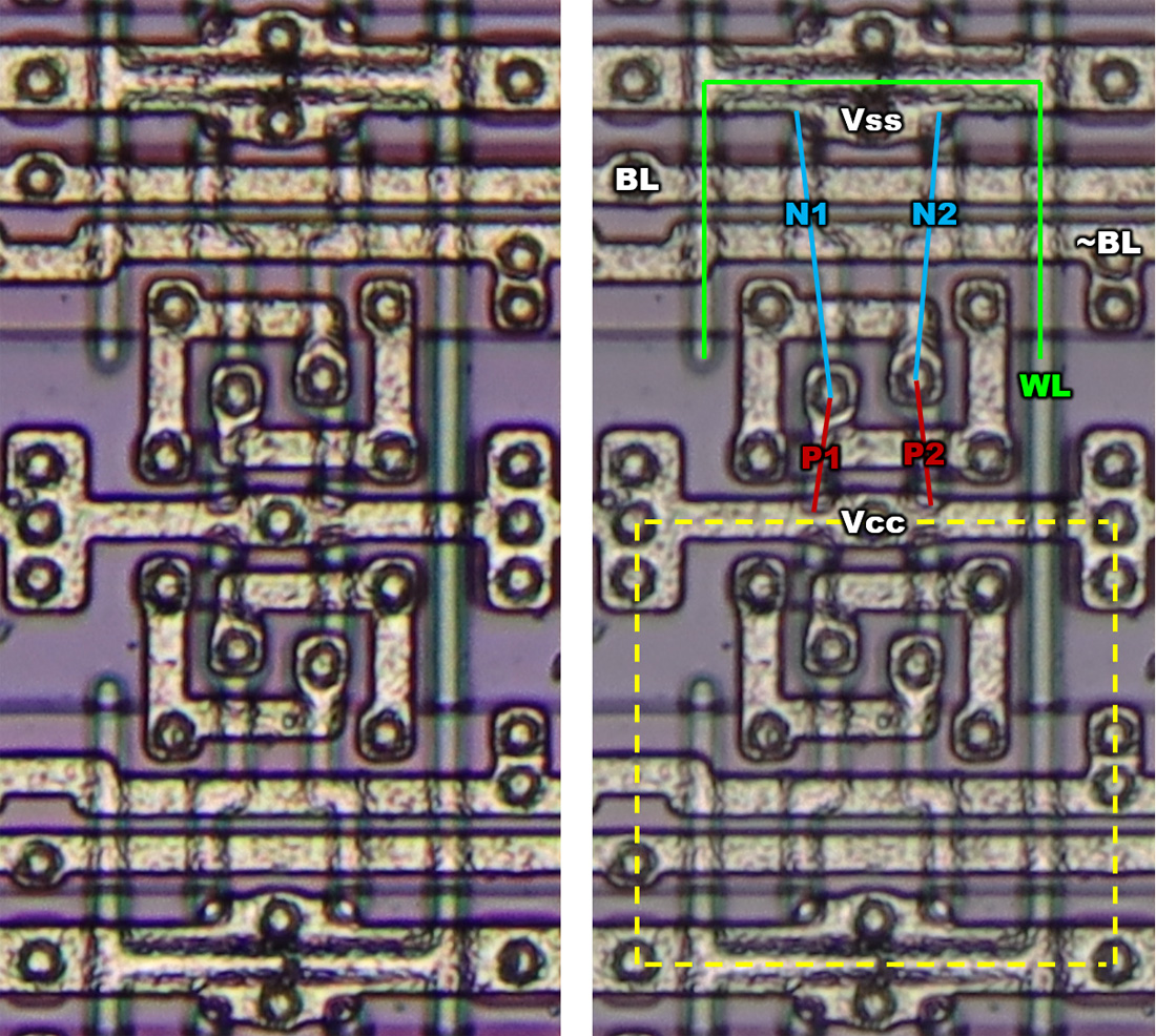
The SRAM cells consist of six transistors. Vertical word lines activate one of the columns (green). The cell can be written to and read from via the horizontal lines BL and ~BL. The memory cell itself consists of the familiar cross-connected combination of two NMOS and two PMOS transistors.
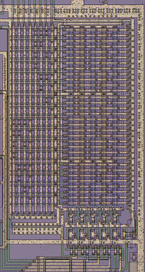
In the upper-right section of the die is the programmable logic array, which can be used to efficiently utilize Port O. The datasheet lists the control of 7-segment displays as a typical application.
https://www.richis-lab.de/uC14.htm 

 Home
Home Help
Help Search
 Login
Login Register


