Author Topic: 68010 custom computer build  (Read 3764 times)

xrunner and 16 Guests are viewing this topic.

Online paulcaTopic starter

  • Super Contributor
  • ***
  • Posts: 6358
  • Country: gb
Re: 68010 custom computer build
« Reply #25 on: September 03, 2026, 05:15:41 pm »
Interesting debug on the ROM programmer.  Helped by claude for number crunching while I feed it copy pasta from datasheets.

Problem:  Spuratic write failures.  Random addresses, clustered in time.  No errors for a full sweep of random write/read/verifies across the whole chip.  Then the next past a cluster of 4 or 5 failed writes, "0xFF" default erase value.

My first test was to lift the board while running error free and stuff my fingers onto every pin I could, really "finger roll it".  Underside too.  Brought the flurescent light down an inch from it and power cycled it.

It didn't flinch or drop a bit.

So I moved to timing.  Asked claude if the delay loop it wrote was tight.  It was.  Did it also include the '245 transsciever switch, drive and settle times?  Nope.

So it number crunched those from the timing table I copy pasta'd to it.  Then it ran a delay loop calibration thing, a gcc builtin? on the STM32F411.  Produced a delay table.  Implemented.

Still a cluster of errors only 25% through the first sweep.

So I told it to leave the documentation for those delay values in place and state that we doubled them for engineering grace.

Still no errors this pass.  However.  It's now, both chips, full 512Kbyte 0x80000 write, read cycles x2 chips.  Its not at all fast.  Like 15-20 minutes per full write. 

Part of my doesn't care.  It will be a while before I need a ROM anywhere near that size, but part of me thinks the timing, somewhere, is bogus.  Like a stupid HAL_Delay(1) hiding.
"What could possibly go wrong?"
Current Open Projects:  68000 Self Build computer + OS.
 

Online paulcaTopic starter

  • Super Contributor
  • ***
  • Posts: 6358
  • Country: gb
Re: 68010 custom computer build
« Reply #26 on: September 03, 2026, 08:44:21 pm »
68k ROM flash CLI ready. Type 'help' for commands.
Sweep 1: erasing...
Sweep 1: PASS (0x80000 addresses x2 chips)
Sweep 2: erasing...
Sweep 2: PASS (0x80000 addresses x2 chips)
Sweep 3: erasing...
Sweep 3: PASS (0x80000 addresses x2 chips)
Sweep 4: erasing...
Sweep 4: PASS (0x80000 addresses x2 chips)
Sweep 5: erasing...


Sums up how my evening went.  If only it didn't take 30mins per test.  Then again, this is absolutely worst case.  Each byte is a write, then read, low chip, then high chip.  Single threaded.  Writing a straight block and verifying a straight block has WAY less timing delay involved.
"What could possibly go wrong?"
Current Open Projects:  68000 Self Build computer + OS.
 

Online paulcaTopic starter

  • Super Contributor
  • ***
  • Posts: 6358
  • Country: gb
Re: 68010 custom computer build
« Reply #27 on: September 05, 2026, 08:24:40 am »
Feet dragging time again...

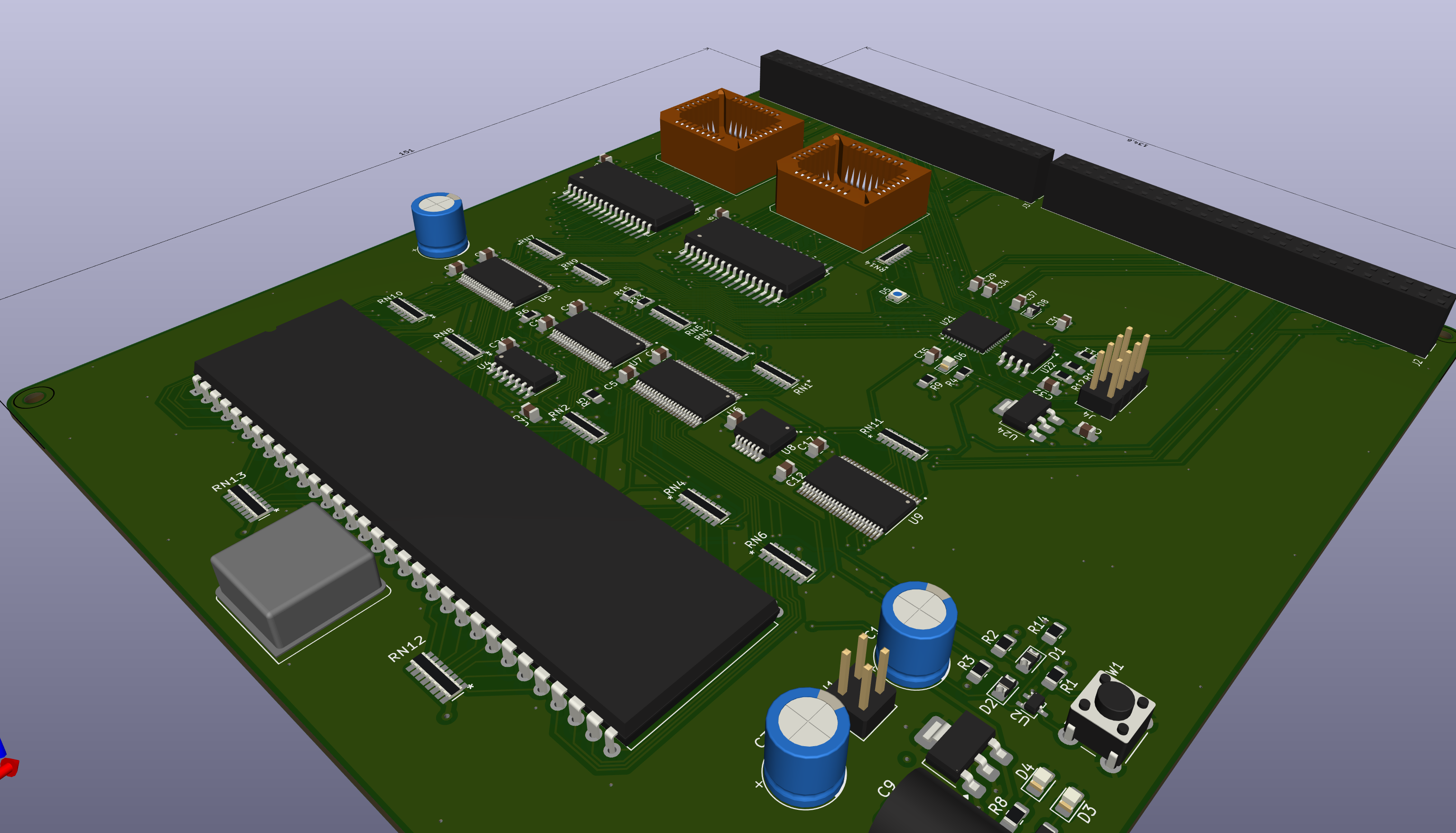
I have this routed with 0 warnings DRC/ERC, could use a bit of labelling on the silk.  Its a fully SBC bootable computer.  5V CPU, 3v3 everthing else.

But...  I'm procrastinating now.  The board has ZERO input or output except the IDC headers which exports an 8bit IO bus. 

Im basically setting myself up to debug a blind, headless PCB.  If it works and I attack something to that IOBus it might say "Hello world", but if it doesn't work.  Its going to be formidable to work out why.

As a minima if it's "going to press", I need to add as many test points as the route will permit.  They will be scattered to the 9s but there is plenty of room around to route edges if I can catch signals in the open for a test point.  The header itself covers a good 75% of important test points.


Period UART is already out.  The board is firmly 3v3 beyond the CPU and I spent a lot of time and effort ensuring that.  So it's a 3v3 UART ... or I2c... or SPI.... or why not an STM32F411 doing all of the above on that io bus?  Because none of that part is tested yet.  The FPGA in circuit is deliberately small and deliberately only there so I can get a few mistakes in the address glue and DTACK timing without a board respin.   It does not have the IO to run a UART.

I want to get this board "Out of the way" as it's blocking the 'real' board building, as it tests a lot of things in concert.  If they work, the board basically gets cut in four.  CPU+Transciever on one PCB.  Memory/FPGA on a Memory card.  Powersupply and bus pulls on the interconnect/backplane.  Then I can add as many IO cards or experiements as I like.
« Last Edit: September 05, 2026, 08:27:03 am by paulca »
"What could possibly go wrong?"
Current Open Projects:  68000 Self Build computer + OS.
 

Online paulcaTopic starter

  • Super Contributor
  • ***
  • Posts: 6358
  • Country: gb
Re: 68010 custom computer build
« Reply #28 on: September 14, 2026, 02:50:56 pm »
So this arrived.

2911822-0

2 hours of placing and abracadabra:


In review.  Those RNetwork footprints provide zero margin for error.  Like none.  When placed the castled edges barely touch pads on both sides.  Some did not make bond on both sides, but most did.  The FPGA looks like it doesn't even need touched up or reworked.  The LVC level shifters I can see are going to be a pain as always.

Just a coupled of caps which escaped solder paste somehow and the through hole stuff to go.
« Last Edit: September 14, 2026, 07:20:42 pm by paulca »
"What could possibly go wrong?"
Current Open Projects:  68000 Self Build computer + OS.
 

Offline SiliconWizard

  • Super Contributor
  • ***
  • Posts: 17773
  • Country: fr
Re: 68010 custom computer build
« Reply #29 on: September 14, 2026, 09:02:08 pm »
I was just thinking - do you have a means of uploading code to RAM without having to re-program EPROMs? That sure would make development much easier.
 

Online paulcaTopic starter

  • Super Contributor
  • ***
  • Posts: 6358
  • Country: gb
Re: 68010 custom computer build
« Reply #30 on: Yesterday at 07:49:21 am »
I was just thinking - do you have a means of uploading code to RAM without having to re-program EPROMs? That sure would make development much easier.

Its the immediate goal after it boots, but it needs the IO header and the IO board is still in KiCAD.

The most this board is going to do is light LEDs on the IO header to tell it's booted or not.

For V2, it going modular, but the memory card won't have any ROM.  It will just have the FPGA memory "controller" contain a bootloader and enough for the CPU to go get it's boot code from an SDCard or similar "disc" surrogate.
« Last Edit: Yesterday at 07:53:25 am by paulca »
"What could possibly go wrong?"
Current Open Projects:  68000 Self Build computer + OS.
 

Online paulcaTopic starter

  • Super Contributor
  • ***
  • Posts: 6358
  • Country: gb
Re: 68010 custom computer build
« Reply #31 on: Today at 12:13:02 pm »
So I reworked the bridges and fixed up the RNetworks. 

The RNetworks are a ___ing curse.  I am changing that footprint for any future use of these, even if it means I can't sneak a via between the pads.  The actual package is about 0.2mm wider than the space between the pads.  If the placement is off by 0.2mm only one side "flows" onto the pads.  It took me an hour to fix them all an I had to resort to some rather janky techniques.  Like "skating them around with the iron until they got aligned and then holding them down with tweasers ... all while the solder was flowing. 

I tried removing them, cleaning it up and hand soldering them but there was just not enough area to even "tack" them down.  The moment you touched the other end it would twist out of alignment.  I tried removing, cleaning up, applying solder paste by hand and air reflowing them...  Not a hope in hell.  They just pulled to one side or other because the air couldnt get both side flowing at exactly the same time.    They are not pretty.

I may have screwed up the footprint, but I was sure I download it from Digikey.  Then again I suppose they are not only in error sometimes, but in others they give NO tolerance and expect machine placed, machine pasted and oven soldered.  0.2mm placement accuracy is a given.

On the other hand.  The many bridges on the LVC transcivers came out with just a touch of the iron.  Only one needed a blob removed with wick.
"What could possibly go wrong?"
Current Open Projects:  68000 Self Build computer + OS.
 

Online paulcaTopic starter

  • Super Contributor
  • ***
  • Posts: 6358
  • Country: gb
Re: 68010 custom computer build
« Reply #32 on: Today at 12:22:54 pm »
The choice to use a small FPGA instead of a crowd of 74 series gates, pays off already.

I found a bug in the signal logic for DTACK.  Specifically with the TAS instruction.  It performs TWO data operations within a single bus transaction.  Or rather, AS is asserted through two data transactions.  The CPU requires you to deassert DTACK in between them.  Not doing so would be undetermined.  Most likely a bus hang or glitched databus.

That becomes a lot easier to fix.  Its a single line of verilog to change the signal set which clears the DTACK register from "AS" to UDS|LDS.  Although you need to rotate it for negative logic and positive clocking.

This is a similar cousin circuit on the IO board in design.  Its also getting closer to the point a small FPGA would help.  The highlighted note is now out of date.
« Last Edit: Today at 12:32:34 pm by paulca »
"What could possibly go wrong?"
Current Open Projects:  68000 Self Build computer + OS.


Share me

Digg  Facebook  SlashDot  Delicious  Technorati  Twitter  Google  Yahoo
Smf