Hi. I'm looking for opinions or advice on my PCB layout.
It's simply an adapter for the STM32L4R9I-DISCOVERY board to allow me to use a large round Panasys MIPI LCD display. It is to go in place of the supplied MB1314 AMOLED smartwatch daughterboard.
So it has a backlight LED driver, basically following the datasheet circuit diagram, and then just tracks between the connectors. Both clock and DSI are high speed differentials. Annoyingly the P/N of the differential pairs always seemed to need to cross over each other! On the big connector they are side by side, but as the LCD panel's connector is double row, they are opposite each other instead!
Things I thought about:
- I could have made use of the bottom layer for more than just one big ground fill. That could have made it much easier to route the tracks. I was trying to keep it simple though and wasn't sure if that was a good or bad idea.
- Number of vias to the ground layer.. too many? not enough?
I suppose once I have one in my hand I will have a better idea of size and where I could have gone bigger or smaller. I will do a print out as well.
I started with the ST schematics, just so I could get the big Samtec connector. That's why it still has their logo on it, and is named 'copy of mb1314' :-)
Here's a PDF:
http://www.internetsomething.com/lcd/pcb/PDF.pdfThe rest (gerbers etc) can be downloaded from this directory:
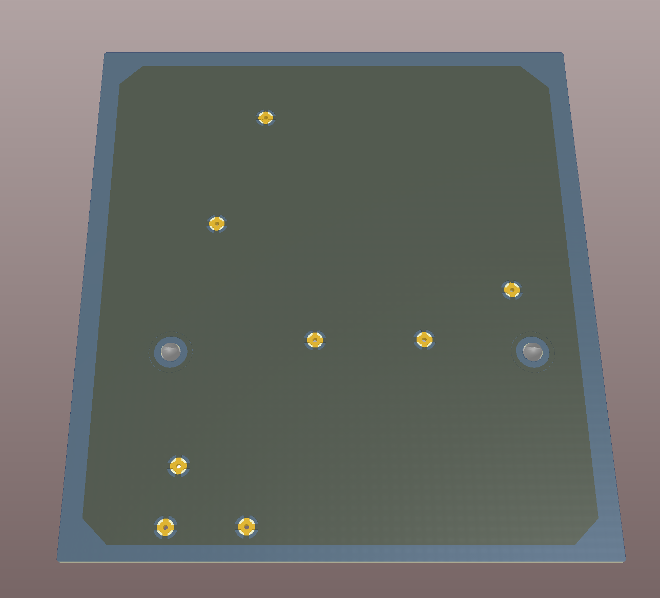
http://www.internetsomething.com/lcd/pcb/and here's 3D pictures:


Any obvious total fails? Other suggestions?


