Weird, what's up with the pads in the middle of the non-pop polymer chip footprints? Are they making them in LGA styles now?
Maybe it's just an alternate placement for some ceramic chips there.
EDIT: I should have guessed, there's already a
thread about this.
Well, you have no idea how relevant this question has become. In a fascinating twist, it seems NVidia might have been a little too permissive in allowing board partners to use the big, cheap polymer caps instead of ceramic chip arrays:
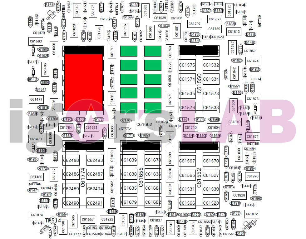
And apparently this is a leading theory for why some cards (which all?/often? happen to use the polymer caps all in 6 positions) become unstable in certain light workloads that permit peakier loading of the CPU (which leads to higher clock frequencies). And so now decoupling capacitors have become a front-and-centre topic in the gaming hardware community:
link + countless YouTube videos that I won't bother linking. Never thought I'd see YouTube commenter gamers saying they'll insist on cards with MLCCs only!
I wonder at what point it becomes economical to use dielectric-loaded PCB layers. They've got a few thousand capacitors on there, I would guess. Well, apparently this still isn't to that point... (Embedded or carbon-ink resistors too, for terminations and such. That was an IBM thing, among others, don't know that it's ever been used on PC gear though.)
I thought the space between layers, while thin by any normal definition, are so thick compared to the layers in an MLCC that that'd not add up to much. But I suppose the huge area, plus the fact that the ESR/ESL is practically exactly zero, could be helpful.
BTW, I always appreciate your messages so much Tim!


