Author Topic: Different die pictures  (Read 87032 times)

0 Members and 1 Guest are viewing this topic.

Offline NoopyTopic starter

  • Super Contributor
  • ***
  • Posts: 1736
  • Country: de
    • Richis-Lab
Re: Different die pictures
« Reply #300 on: June 26, 2023, 09:45:55 am »


Here you can see a finished A231. The letters MD are ambiguous. They can stand for October 1963 or December 1980. In this case, it is certainly December 1980.


The datasheet contains just a block diagram of the A231. As an RGB matrix, the A231 generates the three color signals in analog color televisions from the luminance signal and the two color difference signals. The block diagram also includes a reference voltage source and a dark keying circuit.


A detailed circuit diagram of the A231 is shown in Radio Fernsehen Elektronik 5/1978.


The die in the A231 housing is exactly the same size as the individual elements on the mask (2,2mm x 1,7mm) within the tolerances. The characters 02A231 are shown on the upper edge. Consequently, this is the same revision that is also shown on the mask.


There is also a die that has been sorted out. In the center, you can still see the remains of the colored dot that marks the die as a reject. This is also the second revision and there are no other special features.


With the real circuit, one can now also take a closer look at the structures of the mask. Here, the areas that are p-doped as part of this process step are colored.


You can also invert the mask to mark the areas that will be left out by the p-doping.


On the left and on the upper edge there are two points each (yellow), which are used to place the individual masks exactly on top of each other. In the lower left corner, further structures show how well the masks are aligned against each other (orange).

No p-doping is introduced under the bondpads. Only in the upper left corner the mask defines a p-doping (green). The reference potential of the A231 is supplied via this bondpad. The p-doping connects the reference potential to the substrate and ensures that the individual wells of the device remain isolated from each other.

The resistors are represented by strips of p-doping (pink). Thin strips have larger contact areas at the ends. Thick strips can be contacted without special geometries.

The NPN transistors (blue) are of different sizes. They have a strip of p-doping as a base area. Partly there is an additional narrow strip in the corresponding wells, which can be used as a resistor or for crossing lines.

In the left area there are two PNP transistors (red).


The two NPN transistors T24 and T25 are shown here as examples. As described, the p-doping forms the base areas of these transistors, into which the emitter areas are then introduced. The additional stripe in the upper transistor represents the resistor R29.


The outputs of the A231 are equipped with large NPN transistors. The large collector contact can be seen on the left under the metal layer. In the large base area there are three emitter areas, in the spaces between which the base potential is supplied.

In the lower area a square can be seen, which represents a driver transistor. The emitter area can be seen a little better in other pictures. Together the two transistors represent a Darlington pair.


The double structure in the left area of the die generates the two PNP transistors T31 and T32. Usually the smaller p-doped area in the center of such a structure is the emitter, here the collectors are located there. The large p-doped rectangle forms the common emitter. The n-doped well represents the base area.

From the emitter rectangle a stripe leads to the transistor T52, which seems to be overlaid by the strong n-doping of the NPN emitters. As a pinch resistor, this structure provides a relatively high resistance value. The resistor is not mentioned in the schematic.


https://www.richis-lab.de/maske01.htm

 :-/O
 
The following users thanked this post: xrunner, RoGeorge, ch_scr

Offline NoopyTopic starter

  • Super Contributor
  • ***
  • Posts: 1736
  • Country: de
    • Richis-Lab
Re: Different die pictures
« Reply #301 on: July 06, 2023, 10:57:47 am »


The XR2206 is a function generator from Exar that covers a frequency range from 0,01Hz to 1MHz. The device can generate a sine, a square wave, a triangle signal and a ramp. Amplitude, frequency and duty cycle can be modulated. The supply voltage may range between 10V and 26V.


In the datasheet a block diagram shows the integrated function blocks. The base is a VCO, a voltage controlled oscillator. The clock frequency is defined by an external capacitor at pins 5 and 6 and external resistors at pins 7, 8 and 9. With a fixed capacitance value a frequency range of 2000:1 can be swept. Via inputs 7, 8 and 9

The square wave signal is output directly. The VCO also feeds a sine converter. The connection is not shown. Depending on the position of switch S1, the function block supplies a triangle or a sine signal. Pins 15 and 16 can be used to adjust the symmetry of the signal. R3 influences the level of the triangle or sine signal.


The datasheet also contains a complete circuit diagram of the XR2206.


The dimensions of the die are 2,6mm x 2,2mm. The metal layer shows the designation 2206. The numbers 05 in the upper right corner cannot be assigned directly, perhaps it is a revision counter. In the silicon, there is the string M5145. Maybe the basic design is used for another device. This theory is supported by the fact that quite some elements are not connected in the XR2206.


The non used elements and the large structures give us a very clear picture of the structures of the different components.


https://www.richis-lab.de/gen03.htm

 :-/O
 
The following users thanked this post: RoGeorge, ch_scr, MegaVolt, iMo

Offline NoopyTopic starter

  • Super Contributor
  • ***
  • Posts: 1736
  • Country: de
    • Richis-Lab
Re: Different die pictures
« Reply #302 on: July 20, 2023, 08:40:23 pm »


Motorola developed the Optobus, a system that should make it possible to use the large bandwidth of optical fibre connections without the usually high investment. The IEEE paper "A Low-Cost High-Performance Optical Interconnect" states a target of $300/GBit. In Motorola's application note AN1572, there is even a figure of $100/GBit for a high volume production run. Motorola had a website for the Optobus system which contains the specifications of the Optobus module. A transmission rate of 4GBit/s over 300m is specified. Strictly speaking, it is 10Bit transmitted in parallel at 400MBit/s.

The Optobus system was apparently never produced in a larger quantities. In the magazine Electronic News Vol. 40 (November 1994) you can read that series production was supposed to start in the third quarter of 1995. The transceiver shown here must still be a sample. It was produced in June 1994. As will be shown later, the construction does not yet correspond to the series production. There are many IEEE articles on the Optobus system, some of which contain different specifications. They apparently reflect the development of the transceivers.

 The Motorola website also contains information on the successor Optobus II, which was supposed to enable a transmission rate of 8GBit/s over 200m. The IEEE paper "OPTOBUS I: Performance of a 4Gb/s Optical Interconnect" (1996) mentions that the Optobus II modules should be available at the end of 1996, only shortly after the Optobus I system.


Application Note AN1572 shows for which bandwidths and distances the Optobus system is suitable and for which areas it should be developed further.


The IEEE article "OPTOBUS I: Performance of a 4Gb/s Optical Interconnect" shows a rough block diagram of the device. It is a transparent interface. The input signal controls a laser diode, whose signal is evaluated by a photodetector and output again. The switching threshold is fixed.


Application Note AN1572 shows the function blocks in more detail. These are two 10Bit wide interfaces. One interface is used for sending, the other for receiving data. Only one transmission direction is shown here.

The transmitting side contains special laser drivers. The receiving side has four stages. The first stage is a transimpedance amplifier that converts the current of the photodiode into a voltage. The second stage amplifies the signal, which is evaluated in a third stage. Special output drivers finally output the transmitted data differentially.


The dimensions of the Optobus module are 3,7cm x 3,9cm. It is a pin grid array (PGA-196) with 96 pins on the underside. 40 pins carry 10 differential input signals and 10 differential output signals. The other 56 pins are connected to the supply and reference potentials and ensure that the high frequencies remain controllable. In addition, the many pins improve the heat dissipation of the module. Motorola's Optobus website assigns 101 pins to the module. Apparently, five more pins have been added to the series version.

As you can clearly see, this is a used module that was already soldered into a circuit board. When the module was removed from the board, some of the pins were torn out of the pin grid array.


In the upper left area, the placement print represents some strings that can only be partially assigned. MCM-L stands for "laminated multichip module". Formation B could indicate a second revision. 9351 probably represents a datecode.


The board has an edge length of 3,56 cm. There is no solder resist on the top side, so that you can partly see the traces in the second layer. The copyright in the upper right corner refers to the year 1993, which matches the datecode in the assembly print on the back.

On the upper edge, the two components that represent the optical interfaces stand out. They are made of a translucent polymer. A more detailed analysis of these elements will follow. The right-hand component was soldered off the board and then reattached with hot glue. Probably one wanted to keep the optical appearance to some extent.

Motorola attached the integrated circuits as bare die to the board and connected them electrically with bondwires. Most of the bondwires are already bent and torn off.


In order to be able to present a transceiver module that is as cost-effective as possible, a common FR4 board material was used. The layer structure is described very differently in the various IEEE articles. Presumably they reflect the further development of the module:
"Parallel Optical Interconnects Using VCSELs" (August 1995): 7 layers, 4 of them with 70µm.
"Characteristics of VCSEL Arrays for Parallel Optical Interconnects" (May 1996): 4 layers, 2 of them with 70µm
"A Low-Cost High-Performance Optical Interconnect" (August 1996): 8 layers, 4 of them with 70µm

The many layers were necessary to guarantee sufficient signal integrity. The high copper content has a positive effect on heat dissipation too. There are also different specifications for the power dissipation of the module:
"Parallel Optical Interconnects Using VCSELs" (August 1995): 1,7W.
"Characteristics of VCSEL Arrays for Parallel Optical Interconnects" (May 1996): 1,5W
"A Low-Cost High-Performance Optical Interconnect" (August 1996): 1,6W
Optobus website of Motorola: 1,35W

In detail, you can see the glass fibre mats embedded in the epoxy, which consist of longitudinal and transverse interwoven bundles. In the upper and lower areas, the bundles are thinner and are correspondingly closer together. At these levels, the parasitic properties are more homogeneous, which is advantageous for very fast signals. Whether this fact was relevant here or whether the layers simply resulted that way remains open. A layer structure cannot be clearly recognised in these images.


If one grinds the board at the lower left and right corners up to the first vias, these pictures emerge. Seven layers are visible. This is unusual, as boards are usually built symmetrically. The thicknesses of the copper layers are also asymmetrical here. In the upper area there are two 35µm copper layers, while most of the other layers have a thickness of 70µm. The bottom layer is a little thicker at 105µm.


This transceiver is obviously a development model. The IEEE articles describe that it was planned to encapsulate the circuit carrier. The shape of the housing was obviously also adapted in this context.

(Left: "Handbook of fibre optic data communication" Middle: IEEE "OPTOBUST: A Parallel Interconnect Solution" Right: Motorola Optobus website)


The IEEE article "A Low-Cost High-Performance Optical Interconnect" describes the construction of the series module in more detail. According to this, a dam is placed in the outer area of the board, which makes it easier to encapsulate the electronics completely.

In the picture on the left from the "Handbook of fibre optic data communication" the dam is clearly visible. The layout of the transceiver is slightly different from the module documented here. In the right picture from "Optobus I: Performance of a 4Gb/s Optical Interconnect" again a slightly different revision can be seen. There, the optical modules seem to be constructed differently too.


The two optical components each contain 10 channels. The receiver is integrated in the left half. After the optical signals have been converted into electrical signals, they are first evaluated in the input amplifier (red). Its output signals pass through two output drivers (yellow).

The transmitter of the Otpobus module is located in the right half. A laser driver (green) receives the input signals and controls the laser diodes. A reference voltage source is integrated on the right edge (purple).


[...]

 :-/O
 
The following users thanked this post: T3sl4co1l, doktor pyta, RoGeorge, ch_scr, MegaVolt, D Straney

Offline NoopyTopic starter

  • Super Contributor
  • ***
  • Posts: 1736
  • Country: de
    • Richis-Lab
Re: Different die pictures
« Reply #303 on: July 20, 2023, 08:41:32 pm »


Application Note AN1572 shows the circuitry at the outputs of the Optobus module in more detail. A so-called Current Mode Logic (CML) is used. This is a differential amplifier from which the differential output signal can be tapped. With a total current of 5mA and 50Ω pull-up resistors, the voltage between the outputs is 0.25V. This setup allows rise and fall times of 500ps. According to the IEEE articles, the receiver side of the Optobus module draws a current of between 160mA and 200mA at 5V.


The IEEE article "Parallel Optical Interconnects Using VCSELs" (August 1995) describes that especially the design of the receiver component was challenging. The input capacitance was not allowed to exceed 5pF. The inductance had to remain below 7nH. The receiver can evaluate currents from 20µA. Consequently, signals from 40µW can be detected on the optical side. A little later, the value is reduced to 29µW ("Characteristics of VCSEL Arrays for Parallel Optical Interconnects", May 1996). The IEEE article "OPTOBUS I: A Production Parallel Fiber Optical Interconnect" (May 1997) states that the bandwidth of the front end is 750MHz, which allows for a safe datarate of 400MBit/s. Up to 600MBit/s has already been shown.

The signals are supplied from the top and output at the bottom edge. The die is supplied from the left and right. You can just about see that in the lower area three signals lead to the left and two signals to the right. The other five signals must be in a lower position. This probably explains part of the board's construction, where layers 2 and 4 have a thickness of 35µm, while all other layers are thicker. Layers 2 and 4 were apparently used as signal layers.


To the left and right of the receiver are three capacitor blocks each. Each capacitor offers a capacity of 1nF.


Special resistors are soldered on the right and left side of the receiver. The right resistor has been calibrated.


Despite the solid metal layer you can clearly see the ten amplifier sections. The signal inputs and outputs are in a second row. Towards the outside, 12 ground bondpads have been placed on both sides. Obviously, the component is supplied from the side edges. The different amplifier stages seem to have two separate supplies.

The IEEE article "A Low-Cost High-Performance Optical Interconnect" states that the switching threshold of the device can be adjusted with metallisation and bonding variants. Neither is evident here. However, it could well be that the switching threshold was set with the adjustable resistors.


The IEEE article "Parallel Optical Interconnects Using VCSELs" (August 1995) describes that Motorola's MOSAIC III process was used here. A bipolar 2µm process with a cut-off frequency of 16GHz. The IEEE article "OPTOBUS I: A Production Parallel Fiber Optical Interconnect" (May 1997) reports a 1,5µm process. Motorola's Optobus website specifies a cut-off frequency of 12GHz.

Motorola's document "ECLinPS Data" contains the above picture. It shows the simplified structure of a transistor from the MOSAIC III process. According to this, it is a process with two polysilicon layers, which makes it possible to build very small structures with very small parasitic capacitances, which has a correspondingly positive effect on the cut-off frequency.


The MCA10000ECL gate array datasheet shows a more realistic cross-section of a MOSAIC III transistor.


The design dates from 1993 and the internal designation appears to be E14HZA1.


At least two layers of metal were used. The large surfaces on the side edges could be capacitors that stabilise the supply voltage.


Underneath the receiver component are two output drivers that are very similar to the input amplifier. They each receive five signals and output them differentially.

It is easy to see that there are areas for placing several capacitors.


The similarity between the two output drivers and the input amplifier is clearly visible.


The designations of the input amplifier (top) and output driver (bottom) are just as similar as their structures. Most likely, the same basic design was used for both circuits and only the metal layer was varied.


Also in detail, the structures are very similar to those of the input amplifier. At the same time, the differences can be seen under the upper metal layer. Here, one channel occupies two of the vertical columns.


Both output amplifiers show severe damage. It could be an electrical overload. However, it could also be that the non-optimal handling over a long period of time has promoted corrosion effects.


Even on the surface, the laser driver looks very different. However, the signal routing is very similar. The ten differential signals arrive from below and are output upwards as control signals for the laser diodes.

The IEEE article "Parallel Optical Interconnects Using VCSELs" contains some details about the laser driver. According to this, it consumes up to 120mA when driving the ten outputs with 5mA each. With the worst possible laser diodes, transmission frequencies of 250MHz would still be possible. Speeds of up to 500MHz have been tested.


Application Note AN1572 shows the structure of the laser driver: A current source provides a certain quiescent current through the laser diode. The current threshold at which the laser effect begins can thus be reached more quickly. Depending on the input signal, a differential amplifier passes an additional current through the laser diode and thus modulates the laser beam.


To the right of the laser driver is a balanced resistor. Compared to the resistors of the input amplifier, the construction only allows for a much less precise adjustment. Most likely, the power of the laser diodes is adjusted with this resistor. In order to achieve a high transmission rate, the power should be as high as possible. At the same time, the optical power of the individual laser diodes must remain below 1mW. Higher powers would force increased protective measures.

It can be assumed that the stable voltage of the voltage reference is also used to adjust the light output. Thus, the light output is much less dependent on the input voltage and the operating temperature.


Motorola's Optobus website states that the driver was manufactured using a 1µm CMOS process. In the IEEE articles, the structure width is documented as follows:
"Parallel Optical Interconnects Using VCSELs" (August 1995): 1µm.
"A Low-Cost High-Performance Optical Interconnect" (August 1996): 0,8µm
"Characteristics of VCSEL Arrays for Parallel Optical Interconnects" (May 1996) 1µm

The division of the die into ten areas for the ten laser diodes is clearly visible. Wide supply lines run between the areas, alternately carrying the two potentials.

The IEEE article "Parallel Optical Interconnects Using VCSELs" mentions that there is a total of 3nF of capacitance on the die to stabilise the supply voltage. This makes it clear that the twice four long horizontal strips represent capacitors. Consequently, the laser drivers only occupy the small part of the area in the middle of the die.

In each column you can see two signal lines coming from the bottom and two signal lines going up. As is well known, the input signal is supplied differentially. The two lines leading upwards carry the output potentials of the differential amplifier. The branch that only diverts the control current to earth is also led to the upper edge of the die and connected to the reference potential outside. This measure guarantees operation with as little interference as possible.


Here you can see the wide supply lines of the circuit. The frame structure has its own supply potentials. The large capacitors do not have any special structures.


The driver itself consists of several elements. In the lower area, the input signal is processed (yellow). A little further away is the differential amplifier that controls the laser diode (green). Above this, three current sources are integrated. Two current sources jointly supply the differential amplifier (red). One current source generates the constant quiescent current through the laser diode (blue).


The IEEE article "Parallel Optical Interconnects Using VCSELs" mentions that one can adjust both the quiescent current and the modulation current via bond connections in 0,5mA steps. The structures confirm this. There are 12 wires running through each of the three current sources. On the left side of the die a circuit controls the 24 lines of the current sources of the differential amplifier. On the right side a similar circuit controls the 12 lines of the current sources for the quiescent current setting. In detail, these are probably individual current sources that can be switched on or off. Fittingly, five leads on the left and four leads on the right lead to the side bondpads.

The additional circuitry in the lower area on the right side of the die certainly represents a common bias setting for the input amplifiers.


https://www.richis-lab.de/transceiver03.htm

 :-/O
 
The following users thanked this post: T3sl4co1l, RoGeorge, ch_scr, D Straney

Offline NoopyTopic starter

  • Super Contributor
  • ***
  • Posts: 1736
  • Country: de
    • Richis-Lab
Re: Different die pictures
« Reply #304 on: July 29, 2023, 08:30:39 pm »
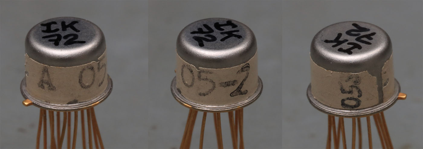
It seems I have postet the IK72 before I startet to post the parts here in the EEVblog-Forum. Now that I have a second (different) IK72 lets talk about both.


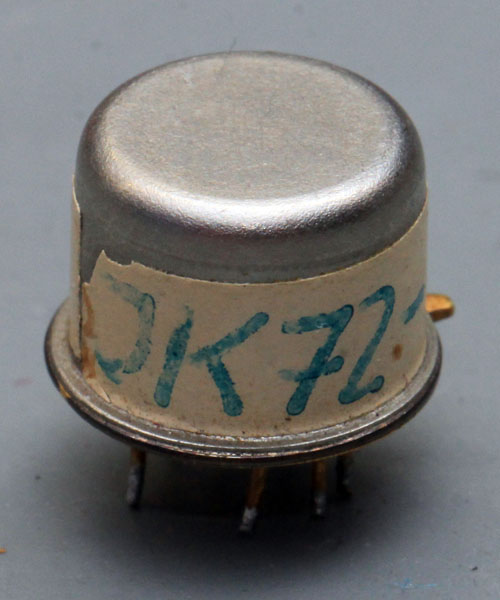
The IK72 is the first monolithic integrated analogue circuit developed in the GDR. The development took place in the R&D department of the Halbleiterwerk Frankfurt Oder (HFO) in Stahnsdorf. The first components were available in 1972. The IK72 represents a differential amplifier including a current sink that can be used for various circuits. Compared to a discrete differential amplifier, an integrated differential amplifier has the great advantage that the transistors have very similar characteristics and also operate at relatively the same temperature levels.

Very little is known about the IK72. The information available online so far was limited to a circuit example from an RFE magazine (1974/18). According to this, the IK72 contains a differential amplifier consisting of two transistors with a third, common transistor at the emitters. However, the article also points out in this circuit diagram that "only the wired parts are shown".

The model seen here is marked with a paper banderole and comes from a developer who should develop a PLL circuit in 1975. It is therefore almost certainly a real IK72.


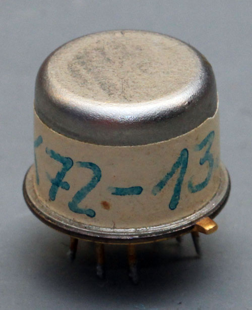
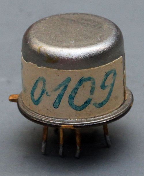
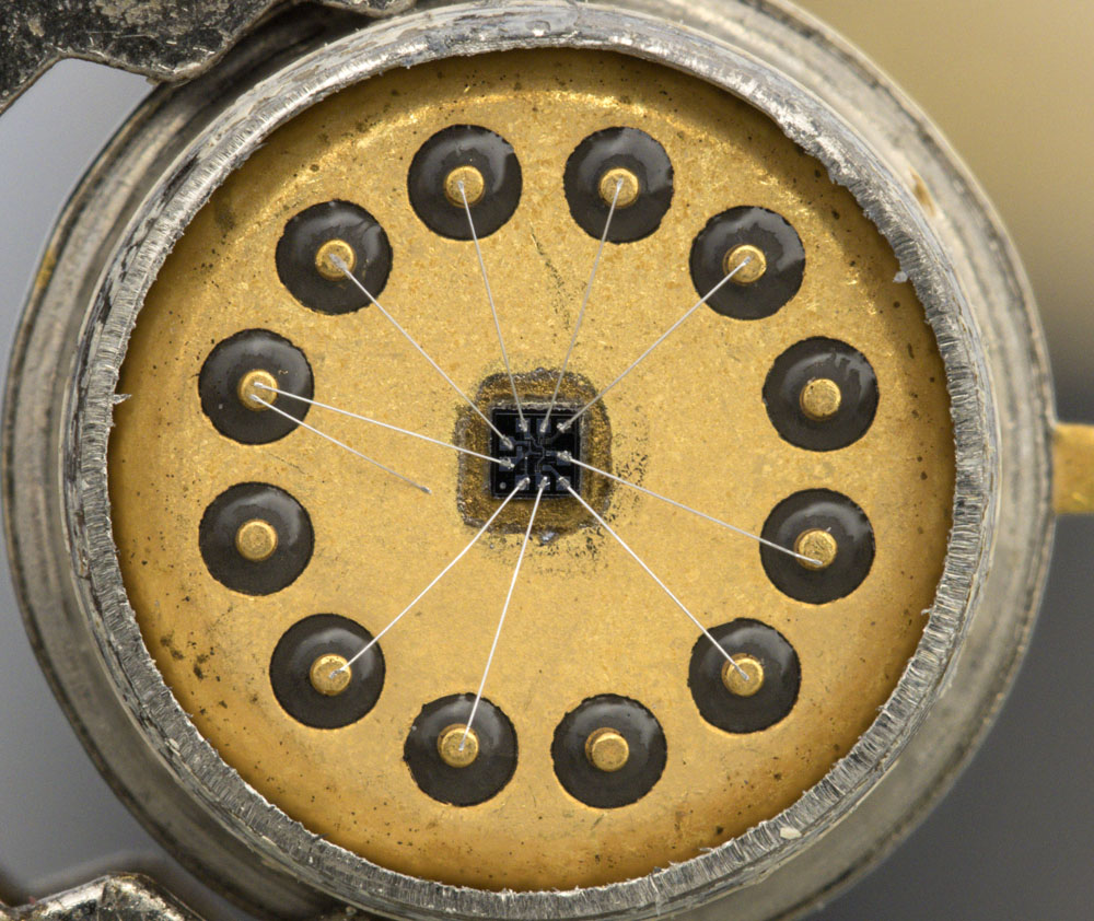
The full designation is IK72-13 0109.


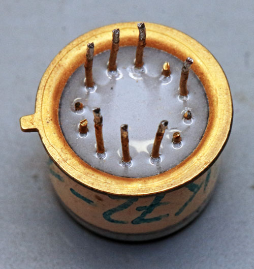
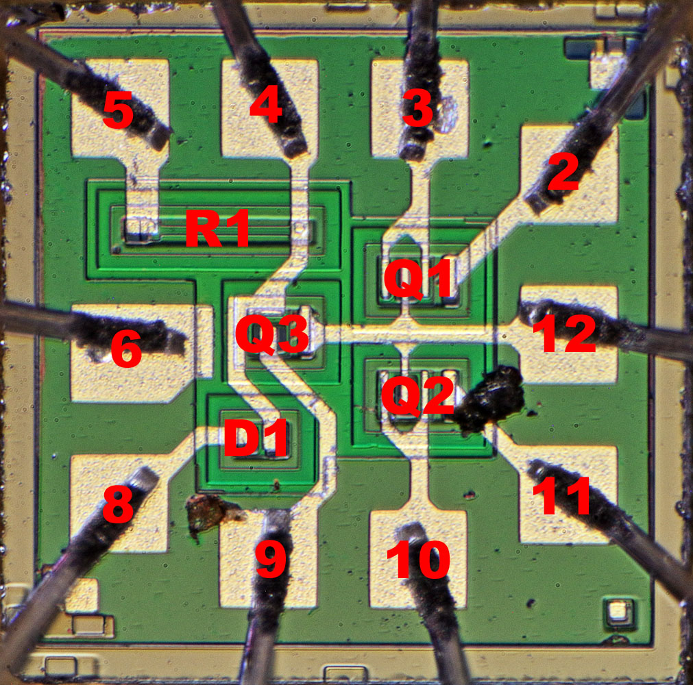
The package has 12 pins. Some of them were cut very short on this component.


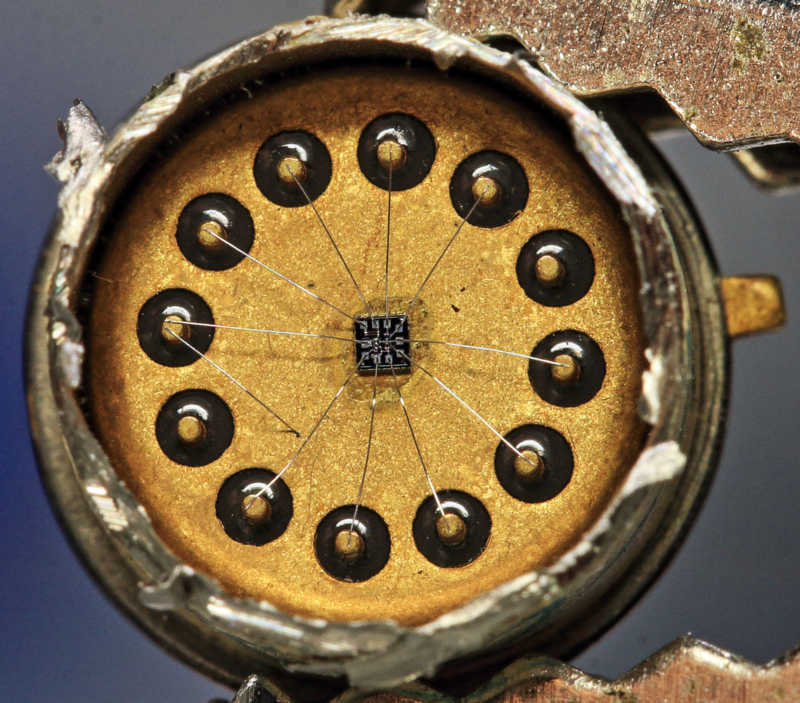
Inside, it shows that 10 of the 12 pins have been connected to the die. One pin additionally defines the housing potential.


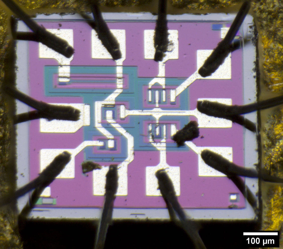
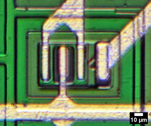
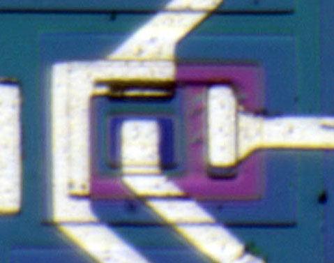
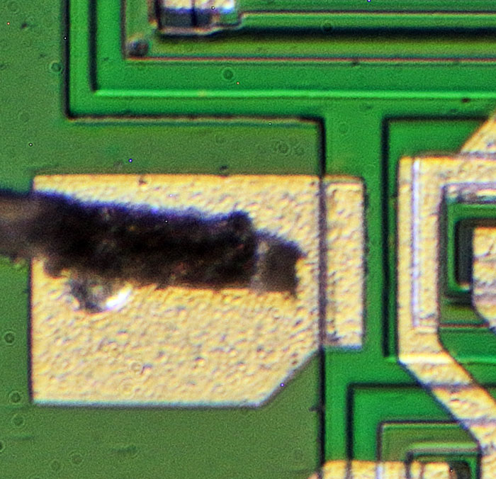
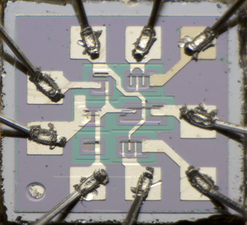
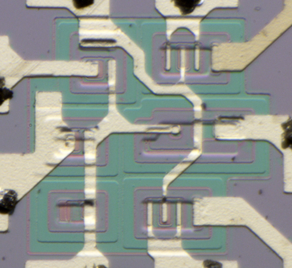
The dimensions of the die are approximately 0,7mm x 0,6mm. There are two particles on the die that cannot be removed with compressed air or by rinsing with isopropanol. Mechanical cleaning could damage the bondwires and should therefore be avoided for the time being.


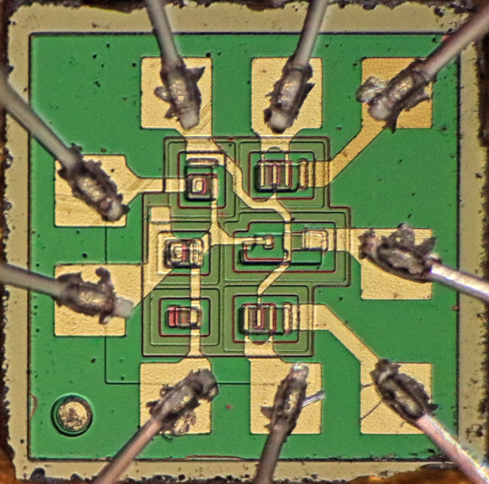
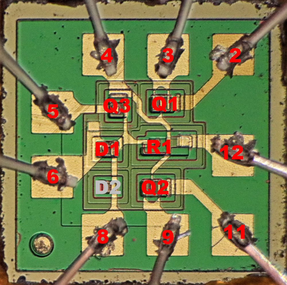
The die houses five elements. On the right are two symmetrical transistors which, with connected emitters, constitute a differential amplifier. To the left is another transistor that can be used as a current sink, for example. In the lower left corner, another transistor is connected as a diode. In the upper left corner there is a resistor.

Geometric shapes are placed in the corners of the dies, which probably facilitate the positioning of the masks and enable a check of the manufacturing process.


The minimum structure width is in the range of 5µm.


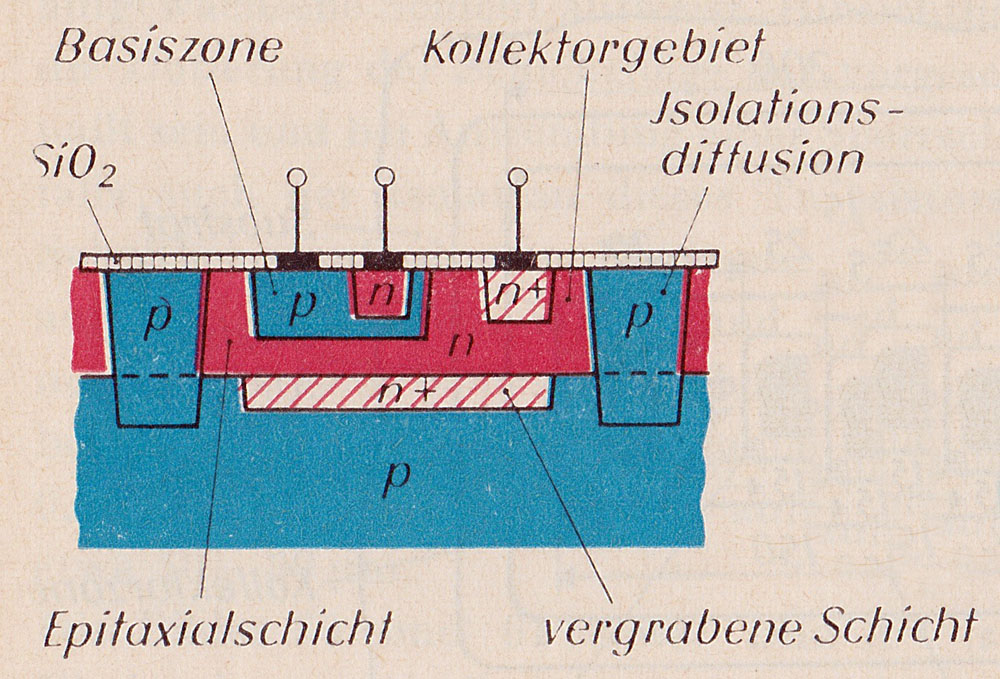
The book Mikroelektronik by W. Glaser and G. Kohl (1970, Naumburg) shows how NPN transistors were usually constructed at that time. The construction of today's bipolar transistors is not fundamentally different.

The basis is a p-doped substrate (blue). A heavily n-doped layer is created where the transistor is to be created later (red/white below). This layer later ensures that the collector potential is transferred from the collector connection to the active area with as low an impedance as possible. A uniform n-doped layer is then applied to the substrate (red), which represents the actual collector. To isolate different transistors and other elements from each other, deep, p-doped frame structures are built up. The resulting pn junctions prevent unwanted current flows across the die. Next, a p-doped base well can be placed in the delimited, n-doped collector area. Finally, the n-doped emitter area is placed inside this base well.

Between the steps described, many intermediate steps take place, which make it possible to form the individual areas as they are shown here. These include, for example, the application, exposure, partial and complete removal of photosensitive layers, the generation and removal of silicon oxide layers and various other process steps.


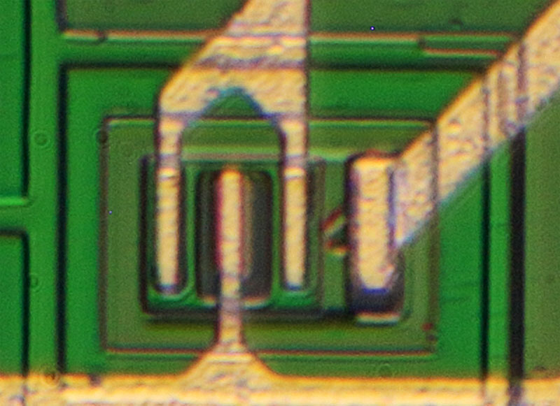
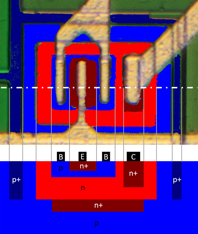
Based on the usual manufacturing process, one can try to assign the visible structures of the IK72 transistors to their functions. A coherent frame can be seen around all active elements, which certainly represents the heavily p-doped insulation. Between the n-doped collector and the isolation frame there is one more area than shown in the schematic above. Often there is still a p-doped zone around the active elements, this must also be the case here. Inside is the n-doped collector area. Below the collector connection, the stronger n-doping can be seen in the connection area. The deeper, stronger n-doping can only be guessed by outlines. To the left of the collector connection is the p-doped base area. This surface is contacted twice. This design reduces the resistance of the base contacting and thus increases the maximum possible switching speed. The n-doped emitter area is then integrated within the base area.


The third transistor, which can be used to realise a current sink, for example, has a slightly different structure than the transistors of the differential amplifier. The basic sequence of the differently doped layers is the same, but there is only one base connection (at the top) and the structure is more square, which means it takes up less surface area. Most likely, this design has a lower cut-off frequency.

In its simplest function, the transistor only controls a constant current, where slightly worse properties are hardly relevant. However, if two of the differential amplifiers are used in an analogue multiplier, the demands on the lower transistor can be as high as on the upper transistors.


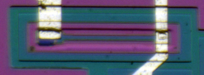
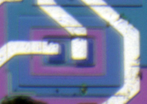
In the upper left corner of the die, a resistor was integrated.


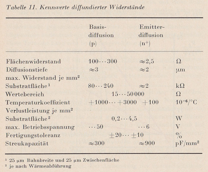
The aforementioned book Microelectronics also presents typical specifications of integrated resistors.

Resistors can be realised with the help of the p-doped base material or with the help of the n-doped emitter material. The two materials cover different resistance ranges. In the BA222 (https://www.richis-lab.de/555_25.htm), the different types of resistors can be seen in real life.


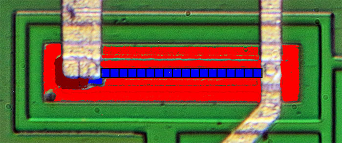
The left feed of the metal layer contacts not only the strip of base material (blue) but also a presumably strongly n-doped area (dark red). Via this path, the n-doped well (red), in which the resistor is located, is connected to a defined potential.

The interconnection on the die makes it possible to measure the resistor from the outside, whereby a value of 2,08kΩ can be determined. There is room for 18 squares in the area of the resistor. With the 2,08kΩ, this results in a specific resistance of 116Ω/sq, which fits quite well with the above characteristic values for a basie diffusion.

The dimensions of the resistor can even be used to estimate the load capacity. With a length of 140µm and a width of 9µm, this results in an area of 0,00012mm². According to the table above, you can expect a power handling of 0,25mW to 5,7mW. What sounds like a very low value can be quite sufficient at the base of a transistor.


At the base of the lower transistor there is a transistor connected as a diode.


The substrate is contacted by its own pin. The exclusive connection enables the substrate to be connected to a lower potential than is available in the IC itself. As a result, the pn interfaces that isolate the transistors from each other widen, less leakage current flows and parasitic capacitances are reduced.


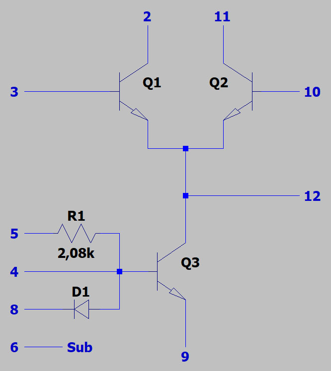
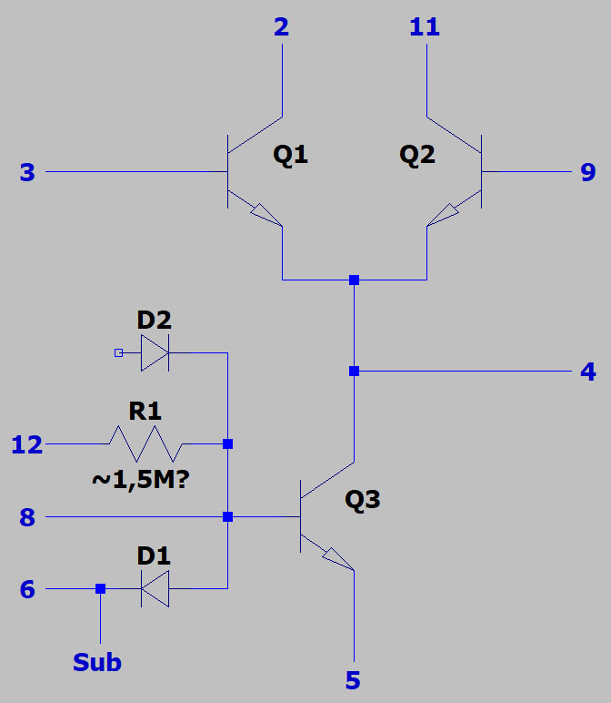
In summary, this results in the circuit shown. The IK72 represents a differential amplifier with a transistor in the emitter path. Transistor Q3 can be used as a current sink or a signal can be applied to it and an analogue multiplier can be built with a second IK72.

The base of transistor Q3 has multiple connections. Pin 4 allows a direct, low-impedance feed-through to the base. Alternatively, resistor R1 can be used as a base resistor. The diode D1, connected in parallel to the base resistor, could make it possible to accelerate the switchoff of the transistor. With this parallel connection, more current can flow from the base, the free charge carriers are discharged more quickly and the transistor switches off faster. However, it is more likely that the resistor and diode in the circuit were used as a current sink to make the current value less dependent on temperature. The temperature drift of the diode then reduces the reference voltage at the base at increased temperature and thus compensates for the drop in the base-emitter voltage of transistor Q3.


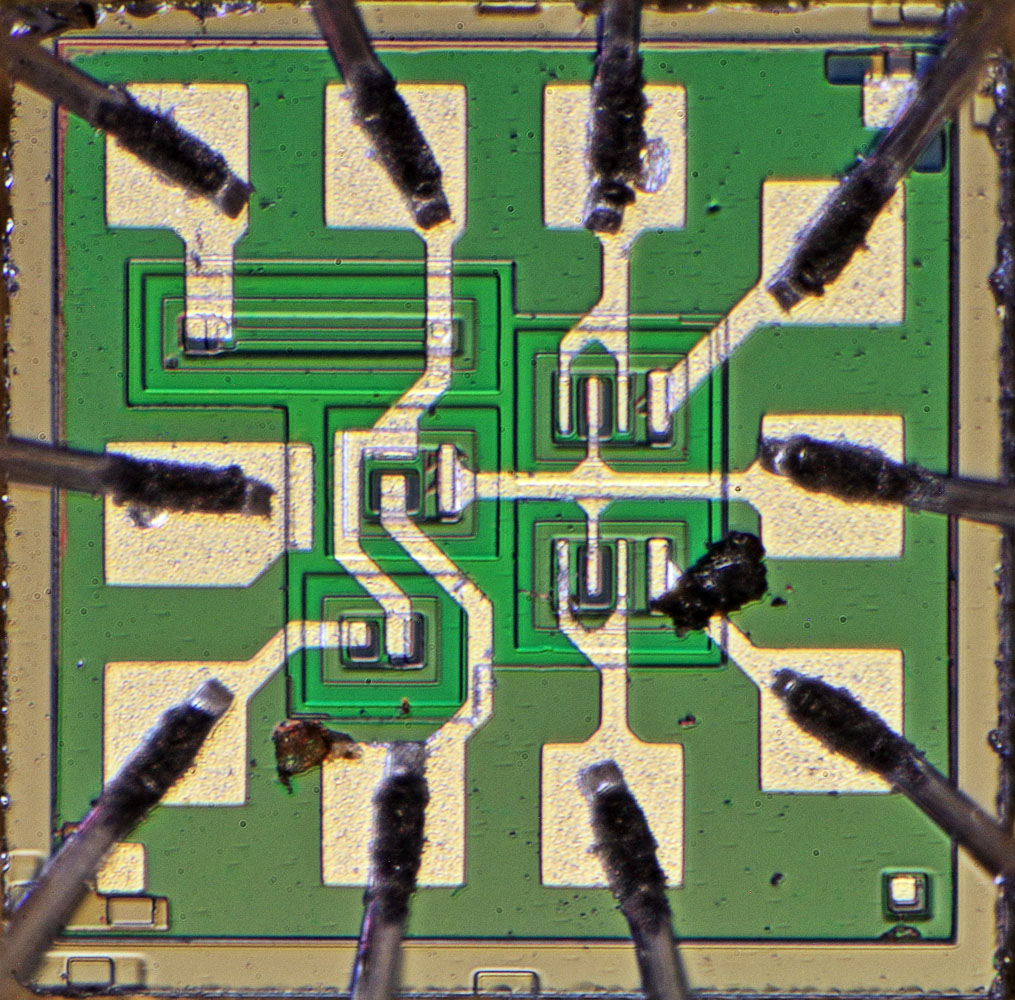
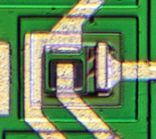
This part should be an IK72 too. The casing matches the casing of the IK72 above. Only the characters "A 05-2" are printed on the paper band. The sequence of characters shown on edge cannot be identified with certainty. It could be the numbers 055.


Superficially, the internal structure is the same as that of the IK72 above. However, pin 10 is not connected to the die.


The edge length of the die is 0,8mm. The construction of the circuit is similar to the IK72 above. In detail, however, there are clear differences.


Unlike the IK72 above, here pin 10 is not connected to the die.


The circuit is basically the same. It is a differential amplifier with some options at the base of the common current sink Q3. The construction and placement of the input transistors Q1/Q2 is the same as the IK72 above. The pinning in this area is similar. However, the remaining pins are pinned significantly differently.

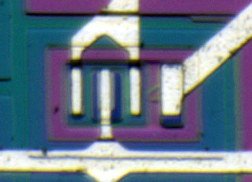
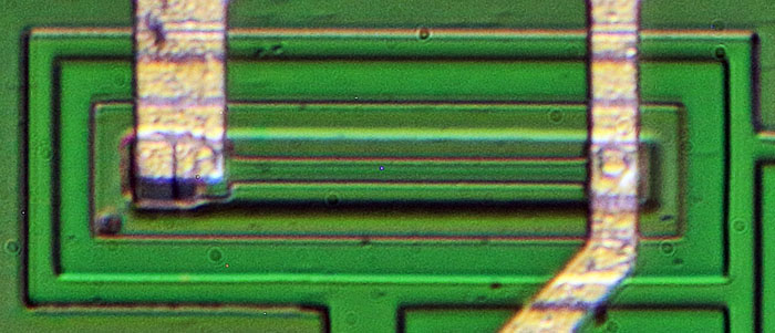
The resistor R1 at the base of transistor Q3 seems to have a surprisingly high resistance value of 1,5MΩ. Perhaps such a high value was not desired. At that time, the integration of resistors was not yet mature.

In this component, there is no separate substrate connection. Instead, pin 6, which contacts diode D1, is additionally connected to the substrate. The die provides an additional diode (D2), but it is not integrated into the circuit.

Perhaps this component is an earlier version of the IK72 or a further development.


The structures of the transistors are clearly visible in detail. The diode D2 seems to have been integrated as a diode only. A collector connection for using the structure as a transistor is not visible. The resistor R1 appears very thin. This would fit the high resistance value.


https://www.richis-lab.de/IK72.htm

 :-/O
 
The following users thanked this post: RoGeorge, ch_scr, iMo

Offline NoopyTopic starter

  • Super Contributor
  • ***
  • Posts: 1736
  • Country: de
    • Richis-Lab
Re: Different die pictures
« Reply #305 on: September 02, 2023, 07:53:39 pm »


Here you can see an RFID sticker as used, among other things, for product identification and as an anti-theft device in retail. The first anti-theft devices consisted just of simple oscillating circuits. In the meantime, however, the cost of RFID chips has become so low that they can be used economically even for low-priced goods. In addition to anti-theft protection, the RFID tags also offer the possibility of storing data and reading it out via radio communication.

The antenna and the RFID chip are located on the back of the label. SML is the manufacturer. The exact designation of the RFID tag can also be found out via the characters "U8" and the shape of the antenna. It is called GB4U8. The datasheet reveals that the RFID chip UCODE 8 from NXP is used here.


The RFID tag's range of up to 12,5m is quite remarkable, but also highly dependent of the direction.


The edge length of the chip can be determined with 0,48mm. According to the datasheet, the UCODE 8 can be obtained as a sawn 8" and 12" wafer. Almost 300.000 RFID chips can thus be obtained from a 12" wafer.


The type of attachment cannot be definitively clarified. The partially transparent material could be a protective lacquer that protects a conductive adhesive or solder connection. However, today there are so-called anisotropic adhesives, which can be applied over a large area and then generates an electrically connection just between the contacts of the chip and the antenna.


The large contacts have a curved contour on the inside. This shape allows a slightly twisted placement on the contacts of the antenna. The smaller pads are electrically isolated, according to the datasheet they only serve to better match the transceiver to the impedance of the antenna.

Between the integrated circuit and the contacts is a 10µm thick polyimide layer, which can be decomposed with increased temperatures.


The UCODE 8 is manufactured with a 140nm CMOS process. The structures are too small to analyze them more precisely. However, it is noticeable that the structure is the same as that of the RFID tag from Race Result (https://www.richis-lab.de/transponder04.htm). Apparently, the UCODE 8 was also used there.


A block diagram is shown in the UCODE 8 datasheet. It shows three basic functional blocks. The front end generates a supply from the received electromagnetic energy, demodulates signals from the transmitter and modulates data to be transmitted to the antenna. The UCODE 8 contains control logic with a relatively large amount of functionality and ultimately an EEPROM as permanent data storage.


https://www.richis-lab.de/transponder05.htm

 :-/O
 
The following users thanked this post: TurboTom, RoGeorge, ch_scr, iMo

Offline NoopyTopic starter

  • Super Contributor
  • ***
  • Posts: 1736
  • Country: de
    • Richis-Lab
Re: Different die pictures
« Reply #306 on: September 11, 2023, 08:51:50 pm »


Two R65C02P4 processors can be seen here. These are the CMOS variant of the widely used 6502 and were produced by Rockwell. P4 stands for the bin, which allows a clock frequency of up to 4MHz. The two devices were purchased from a Chinese distributor. The packages have some peculiarities that give them a suspicious look.

Both chips have exactly the same marking, but the package shape and the package surface differ in some places. For example, only the lower R65C02P4 has two indentations in the upper side and the indentations on the underside are much more pronounced. The upper chip comes from a backend in Thailand. The lower case was made in Taiwan.

The inscription on the lower R65C02P4 is also unclear. Furthermore, it is noticeable that the pin 1 dot is very small and flat. Such conspicuities occur when the surface is abraded. This would also explain why the two large indentations on the upper side are flatter than the one on the bottom.

Both cases show a lot of small damages on closer inspection, especially on the edges. On the upper R65C02P4, the underside appears downright dirty, which does not match the very clean upper side at all. The surface of the pins is irregular. This results from re-tinning, which is often necessary when the surface is oxidized or the components have been desoldered. In addition, some pins are somewhat bent.


The Rockwell R65C02 contains the typical blocks of a 6502 processor.


This die is from the first R65C02. This image is also available in a higher resolution (18MB): https://www.richis-lab.de/images/cpu/08x02XL.jpg. Superficially, the structures fit a 65C02.


The label shows the abbreviation CMD, which stands for California Micro Devices. CMD sold the 65C02 under the designation G65SC02. This designation is partly found here again.

There is a WDC logo too. Behind the abbreviation stands the company Western Design Center, which developed the 65C02 and sells the design to other companies.


Two test structures are integrated on the die, apparently representing an n-channel and a p-channel transistor.


The lower left area shows the revisions of six masks.


The die shown here is from the second R65C02. This image is also available in a higher resolution (22MB): https://www.richis-lab.de/images/cpu/09x01XL.jpg. Superficially, the structures are the same as on the first R65C02. But there are a few small differences.


This processor shows a GTE logo. The company GTE also had a G65SC02 in its program and was taken over by CMD. Consequently, this is the predecessor of the CMD variant.


On this die the revisions of four masks can be seen and also here the WDC logo can be found.


A small difference between the two processors can be found at the data interface on the right edge in the lower area. In the newer device (the upper one), a barrier has been inserted between the controller and the output stages, which is connected to ground.


In the newer processor at the upper left edge the supply was led from the frame structure to the integrated circuit. In this area the output stage for the SYNC signal is integrated.

The highside and the lowside transistor extend a bit to the right. In the newer processor the lowside transistor has been joined by a block, which is connected to the positive supply.


On the right edge is the output stage for the R/W signal. Here, as with the SYNC output stage in the outer area, a block was integrated that carries the positive supply.


Apparently, here two different G65SC02 processors have been refurbished and sold as Rockwell R65C02P4. Thus, they are clearly counterfeits. The three types are basically very similar, since according to Wikipedia Rockwell also took the design from WDC. The processors were functional, consequently had no defect before the refurbishment and had survived the refurbishment itself. However, it is questionable whether their quality was sufficient for the fastest grade "P4". In addition, the previous history and refurbishment reduces the expected remaining life. The effort for the counterfeit is profitable, because this way it seems that there is a larger amount of NOS components and they can be sold more expensive.


https://www.richis-lab.de/cpu08.htm

 :-/O
 
The following users thanked this post: RoGeorge, iMo

Offline NoopyTopic starter

  • Super Contributor
  • ***
  • Posts: 1736
  • Country: de
    • Richis-Lab
Re: Different die pictures
« Reply #307 on: October 10, 2023, 05:18:23 pm »
 
The following users thanked this post: eliocor, PartialDischarge, ch_scr

Offline NoopyTopic starter

  • Super Contributor
  • ***
  • Posts: 1736
  • Country: de
    • Richis-Lab
Re: Different die pictures
« Reply #308 on: October 15, 2023, 03:54:08 am »


With the 1813-0002, Hewlett Packard developed a logarithmic amplifier that was used in the 3575A. The 3575A is a so-called gain-phase meter. It can be used to determine the amplitude and phase of a signal in the frequency range from 1Hz to 13MHz. The inputs offer a dynamic range of 80dB (0,2mV-20V), which can be extended to 120dB with an integrated attenuator.

The module is based on a 25mm x 33mm ceramic carrier with a glued-on metal cover. The ceramic carrier has pins on the side, similar to a DIL housing. For heat dissipation, the assembly is glued onto a metal bracket that offers several screw-on points.


The service manual of the 3575A contains a block diagram showing how to use the logarithmic amplifier. At the input of the meter there is a block with an attenuator and an amplifier. This is already followed by the logarithmic amplifier IC1, which receives the input signal directly and additionally via a level limiter. The IC2 forms a configurable feeback path.

The logarithmic amplifier offers two outputs. The logarithmic output ("LOG") is subsequently fed to a voltage measurement and thus enables a level display in decibels. In parallel, the amplifier offers a second output called "LIMITED". This output is used to determine the phase position between the signal processed here and a second signal.


The service manual also contains a detailed schematic. The logarithmic amplifier is supplied with 2V, ground and -6V. The 2V supply is generated by a separate linear regulator.

The level limiter on the left of the logarithmic amplifier consists of a diode bridge that limits the amplitude to 0,8Vpp. Below this is the unlimited input signal feed and the feedback path, whose frequency response can be influenced via two control lines.

Compared to the block diagram, the outputs are rotated on the right side. The logarithmic signal, which is used for level measurement, is connected to three pins at the bottom. It passes through a relatively complex amplifier. Oscillograms 1, 6 and 7 show the development of the waveform.

In the upper area is the "limited output", which is used to determine the phase position. The control lines that influence the frequency response of the feedback path also adjust the frequency response here. Together, they determine the frequency band to be evaluated, which can be set on the outside of the unit.


The HIGH SPEED DESIGN SEMINAR from Analog Devices shows how a logarithmic amplifier can be constructed. It is a series connection of several amplifiers. The signals of each output are summed and then represent the logarithmic value of the signal.


The functioning of the logarithmic amplifier is based on the fact that the outputs of the individual amplifier stages reach full scale with increasing input level and from then on no longer contribute to the amplification. In the diagram above, Analog Devices shows the behaviour that occurs.

Initially, each stage amplifies the input signal, resulting in a gain factor of N*A. Above a certain input level, the output level of the chain is so high that the last amplifier can no longer set a higher level. From this level on, the chain's amplification factor is reduced to (N-1)*A, since the last amplifier can no longer contribute. As the input level continues to rise, further amplifier stages reach their maximum level and the total gain is reduced to 0. The characteristic curve that sets in thus approaches a logarithmic curve.


The individual parts of the transfer curve are linear, which means that, compared to an ideal logarithmic curve, an error builds up and decreases cyclically.


On the ceramic carrier there is a heart with the hp logo, which was often depicted on Hewlett Packard circuits. The string 1340C could be an internal designation of the design.

In addition to five SMD capacitors and three integrated circuits, there are many extensively adjustable resistors on the ceramic carrier. Test points allow the resistors to be calibrated within the circuit.


It quickly becomes apparent that the hybrid circuit consists of three relatively similar circuits.


To adjust the resistors, some resistor areas were cut and some metal lines were cut. Due to the heat, some of the surrounding elements have become clearly discoloured.


The edge length of the integrated circuits is 0,75mm. There are three identical circuits. Each circuit contains six transistors that are contacted via two metal layers. The string 0302 and a B are found on the right edge. The B represented by the metal layer suggests that different metal layers could be used to represent different configurations of the transistor array.

The transistors have two base contacts, which reduces the base resistance and correspondingly increases the maximum possible switching speed. The transistors are in connected isolation frames In the lower area, a contact can be seen over which one could connect these isolation frames to a negative potential. Here this was less necessary because the substrate is connected to the -6V potential and all potentials in the circuit have a higher potential.


If we analyse the potentials to which the ceramic carrier is connected, we see that the -6V potential is supplied from below and the 2V potential from above. The ceramic capacitors buffer these supplies. In the first block on the far right, the capacitor at the -6V has been omitted.

The non-limited input signal "Input" passes through the right amplifier block 1 and is output in the upper right corner. We will see soon that there are three amplifiers in each block. The input signal that has passed through the level limiter is fed into amplifier block 2, whose output is located at the top edge of the ceramic carrier in the centre. The output signal of amplifier block 2 also serves as the input signal for amplifier block 3. Amplifier block 3 feeds the third output at the upper edge and is simultaneously connected to the "Limited Output" output. The feedback path to the input of amplifier block 2 also closes from this output.


Here the circuit in amplifier blocks 2 and 3 is shown. Each amplifier block contains three amplifiers, which are constructed as simple differential amplifiers with two transistors. The branches with the input transistors drive the outputs, which are combined into a common output signal for each amplifier block individually with resistors.

The second differential amplifier branch of each amplifier contains a voltage divider that generates the input signal for the next amplifier stage. The circuit corresponds to the concept of a logarithmic amplifier described above.

The so-called "limited output" is the output signal of the last amplifier stage. Consequently, it always passes through the maximum amplification. This makes sense because it determines the phase position and in this case only the range of the zero crossing is important. The further you amplify this area, the better the phase position can be determined.

The feedback loop extends from the output of the last amplifier stage to the inverting input of the first amplifier stage.


Amplifier block 1, whose input signal is not limited, also feeds into the "Log Output" node. The first and third amplifier stages are configured and wired like the amplifier stages of amplifier blocks 2 and 3. The configuration of the middle amplifier stage, however, is unusual. It uses the input signal directly, with a voltage divider to adjust the level.

Presumably, these additional amplifier stages serve to correct the errors in the characteristic curve of the logarithmic amplifier.


https://www.richis-lab.de/logamp01.htm

 :-/O
 
The following users thanked this post: doktor pyta, RoGeorge, PartialDischarge, ch_scr

Offline NoopyTopic starter

  • Super Contributor
  • ***
  • Posts: 1736
  • Country: de
    • Richis-Lab
Re: Different die pictures
« Reply #309 on: October 21, 2023, 03:12:29 am »


The component shown here is a 12MHz oscillator built by Siemens. Q95212 seems to be the model designation, but there is no further information about this component. Production took place at the end of 1981.


At the very top of the case is a round quartz crystal.


Metal surfaces are applied as electrodes on both sides of the quartz resonator.


Removing the quartz resonator reveals the oscillator circuit on the bottom of the case. The two strips of sheet metal that held the quartz disc are relatively long so that they provide the necessary freedom for the mechanical oscillation of the resonator.


The Siemens logo shows that the design of the oscillator comes from Siemens itself. A closer look reveals three test structures. In the right-hand area, some elements were not contacted. It is likely that they used these parts to configure the output signal by varying the metal layer.


https://www.richis-lab.de/osc_05.htm

 :-/O
 
The following users thanked this post: RoGeorge, ch_scr

Online RoGeorge

  • Super Contributor
  • ***
  • Posts: 6207
  • Country: ro
Re: Different die pictures
« Reply #310 on: October 21, 2023, 05:53:11 am »
I didn't know there were quartz oscillators packaged in a round metal can, like opapmp.  ???

Are those tin whiskers, at the bottom, downwards from the metal tab?  (in the second picture they are no longer there)

« Last Edit: October 21, 2023, 06:50:26 am by RoGeorge »
 

Offline magic

  • Super Contributor
  • ***
  • Posts: 6783
  • Country: pl
Re: Different die pictures
« Reply #311 on: October 21, 2023, 06:14:42 am »
Is this what it is?


You rotated the die 90° so electrons are falling out ;D
Bottom left is pin 1, bias control or shutdown active low, internal pullup enables the chip.
Pins 2 and 6 are the crystal, and it seems you are supposed to provide external load capacitance here.
Pins 3 and 5 are a differential output, the amplifier uses resistors and current mirrors so it may be linear sinewave.
Pin 4 is ground, pin 8 positive supply. 7 is NC.
 
The following users thanked this post: Noopy

Offline NoopyTopic starter

  • Super Contributor
  • ***
  • Posts: 1736
  • Country: de
    • Richis-Lab
Re: Different die pictures
« Reply #312 on: October 21, 2023, 06:23:51 am »
I didn't know there were quartz oscillators packaged in a round metal can, like opapmp.  ???

Yeah, that´s an old one. There were some in round metal cans.


Are those tin whiskers, at the bottom, downwards from the metal tab?  (in the second picture they are no longer there)

That is one of the packages I opened with the... ... ...I don´t know how you call it in english, such a small metal grinder. Here the company selling them is Dremel or Proxxon. You know what I´m trying to say. And these tools produce some metal flakes...


Is this what it is?
(Attachment Link)

You rotated the die 90° so electrons are falling out ;D
Bottom left is pin 1, bias control or shutdown active low, internal pullup enables the chip.
Pins 2 and 6 are the crystal, and it seems you are supposed to provide external load capacitance here.
Pins 3 and 5 are a differential output, the amplifier uses resistors and current mirrors so it may be linear sinewave.
Pin 4 is ground, pin 8 positive supply. 7 is NC.

Oh no! Perhaps the flakes at the bottom are electron accumulations...  :scared:

Mhm, your circuit and your explanation looks / sounds plausible.  :-+
 
The following users thanked this post: RoGeorge

Online T3sl4co1l

  • Super Contributor
  • ***
  • Posts: 21698
  • Country: us
  • Expert, Analog Electronics, PCB Layout, EMC
    • Seven Transistor Labs
Re: Different die pictures
« Reply #313 on: October 21, 2023, 02:31:29 pm »
"Rotary tool" is the more generic term, though "Dremel" is often used as a genericized trademark(!).

Tim
Seven Transistor Labs, LLC
Electronic design, from concept to prototype.
Bringing a project to life?  Send me a message!
 
The following users thanked this post: Noopy

Offline NoopyTopic starter

  • Super Contributor
  • ***
  • Posts: 1736
  • Country: de
    • Richis-Lab
Re: Different die pictures
« Reply #314 on: November 08, 2023, 07:54:42 pm »


Here you can see the remainings of two 4" wafers. Before a wafer is cut into individual dies, it is placed on a plastic tape, which is still clamped in a holder at this stage. The film has a certain adhesive effect and ensures that the individual dies remain in place during sawing. After sawing, the film can be pulled apart slightly, which increases the distance between the dies and prevents them from bumping into each other when they are removed. The adhesive effect can sometimes be weakened by UV light or heat, which makes it easier to remove the dies.

The tape has been cut out of the holder. The unusable elements, which were marked with a dot during the production of the wafer, were left behind on the foil. These are mainly geometrically incomplete parts and areas to which no structures were applied, as well as a test area. These scrap parts are process-related and cannot be easily optimized. The complete elements that were also provided with structures but were still not usable, on the other hand, reduce the yield and must therefore be optimized to a minimum. Here, the scrap is mainly located in the edge area, where some process steps probably have a more inhomogeneous effect.

The edge length of a die is 5,5 mm. It would be possible to integrate 216 of these chips on one wafer. On the left, 179 elements were usable, on the right 178, which corresponds to a yield of 83% and 82% respectively.


The separation of the integrated circuits has left dark marks on the blue tape.


The edges of the dies are very smooth. This suggests that the wafer was cut completely in one step. There are several alternatives. It is possible to cut the wafer only on the surface and break the lower area by moving the foil upwards. In some cases, the upper area was cut with a thicker blade and the lower area with a thinner blade. This procedure reduces the risk of damage to the edges. More modern processes use lasers to cut the wafers.


The shape of the test area is somewhat surprising. Although the area of the test structures would have fitted easily into the geometry of one die, two elements have been used for it. The right-hand part is empty.


The test area contains many different structures that can be measured electrically. The structures are summarized in 12 groups.


In group B, there are several lines in different planes that cross each other. They are probably used to measure the extent to which signals influence each other at such crossings.

Four transistors can be seen in group D.

Group F contains several elements that appear to be very massive. It is quite possible that these are protective structures for inputs.


Groups H and J contain transistors with different length/width ratios.

The potentials of group L are led downwards. This clearly shows that the same needle adapter was used for all test structures. There are always two rows, each with eight testpads at the same distance. The only exception is the two times three testpads on the right edge, which, however, only contact three longer lines of the metal layer.

The imaging performance of four masks can be evaluated in the upper right area. It is interesting to note that the test structures have been arranged at a 90° angle to each other in order to make any dependencies on the alignment visible.


The testpads of group L contact very large areas. The individual surfaces are connected to just one single line. This indicates that in this area leakage currents to the substrate are determined.


Group A shows three squares in different planes. Four testpads each contact a corner. Perhaps this is a way of determining the homogeneity of the surfaces.

The lowest element in group C contains only one contact. The upper elements could therefore also be different contacts. However, the structures are too small to be resolved.

In the upper area of group E, no elements can be recognized under the contacts of the metal layer. It could be that the properties of the substrate have been determined by this structure. The function of the elements in the lower area remains unclear.


Groups G and I contain further transistor variants.

Group K contains chains of different vias in the lower area, which make it possible to determine the resistances of these vias. A more complex structure reminiscent of a ring oscillator is integrated in the upper area. Ring oscillators are used to evaluate the maximum switching speed of the integrated transistors.


The packaging shows that the wafer was processed at Rood Technology, now RoodMicrotec. RoodMicrotec is a service provider in the semiconductor supply chain. The type designation SCC68692 indicates that it is a DUART transmitter from Signetics. The character string in the bottom line could represent a date code. The wafers would then be from the year 1998.

The date code could be an indication why the SCC68692 was processed by Rood Technology, while the device was still available directly from NXP until the end of 2015. The datasheet was updated in 1998. Although only the omission of a ceramic package is stated as a significant change, there may nevertheless have been changes that made it necessary to store wafers and process them further via a service provider.


With its two UART interfaces, the SCC68692 has a certain degree of complexity.


The handling of the wafers has damaged some of the edges of the dies. The remains of other test structures can still be seen in the saw line. With a little more effort, the properties of the individual elements in the respective area of the wafer can be determined. This is important if you have to deal with increased failure rates that occur always in the same places.


The edge length of the die is 5,5mm. This image is also available in a higher resolution (https://www.richis-lab.de/images/wafer/06x19.jpg 123MB). The lower left corner shows that the Signetics design dates back to 1988. The internal designation appears to be XSC5530A. A bifurcation with a high degree of symmetry is clearly visible.


https://www.richis-lab.de/wafer07.htm

 :-/O
 
The following users thanked this post: RoGeorge, ch_scr

Offline AnalogTodd

  • Regular Contributor
  • *
  • Posts: 90
  • Country: us
Re: Different die pictures
« Reply #315 on: November 08, 2023, 11:13:26 pm »
Here you can see the remainings of two 4" wafers. Before a wafer is cut into individual dies, it is placed on a plastic tape, which is still clamped in a holder at this stage. The film has a certain adhesive effect and ensures that the individual dies remain in place during sawing. After sawing, the film can be pulled apart slightly, which increases the distance between the dies and prevents them from bumping into each other when they are removed. The adhesive effect can sometimes be weakened by UV light or heat, which makes it easier to remove the dies.

The tape has been cut out of the holder. The unusable elements, which were marked with a dot during the production of the wafer, were left behind on the foil. These are mainly geometrically incomplete parts and areas to which no structures were applied, as well as a test area. These scrap parts are process-related and cannot be easily optimized. The complete elements that were also provided with structures but were still not usable, on the other hand, reduce the yield and must therefore be optimized to a minimum. Here, the scrap is mainly located in the edge area, where some process steps probably have a more inhomogeneous effect.
Often, the ones in the center are devices that failed at wafer probe. This is usually due to defects in the parts, whether due to masking issues or silicon defects is usually not reviewed unless yields drop below a nominal threshold.
Quote
The edge length of a die is 5,5 mm. It would be possible to integrate 216 of these chips on one wafer. On the left, 179 elements were usable, on the right 178, which corresponds to a yield of 83% and 82% respectively.

The separation of the integrated circuits has left dark marks on the blue tape.

The edges of the dies are very smooth. This suggests that the wafer was cut completely in one step. There are several alternatives. It is possible to cut the wafer only on the surface and break the lower area by moving the foil upwards. In some cases, the upper area was cut with a thicker blade and the lower area with a thinner blade. This procedure reduces the risk of damage to the edges. More modern processes use lasers to cut the wafers.
The saw is usually done in a single step, and the blade thickness is determined by the thickness of the die. The thicker the cut that needs made, the thicker the blade to avoid warping of the blade during saw.
Quote


The shape of the test area is somewhat surprising. Although the area of the test structures would have fitted easily into the geometry of one die, two elements have been used for it. The right-hand part is empty.
Actually, though it looks empty it may not be. It appears to be a large '+' structure, which was used for mask alignment with stepper tools. With as fine as this process geometry is, you would not be able to get the masks aligned reliably with old optical alignment (via operator checking mask alignment under a microscope).
Quote


In group B, there are several lines in different planes that cross each other. They are probably used to measure the extent to which signals influence each other at such crossings.

Four transistors can be seen in group D.

Group F contains several elements that appear to be very massive. It is quite possible that these are protective structures for inputs.
Actually, group B appears to be structures for measuring metal resistances and via or contact resistances of the process. These are usually very low values so a Kelvin connection needs made to get reasonable results. You can see structures that have sense and force for measuring the resistance of the layer (pads 1,5, 12, 13 and 1, 7, 8, 9) and others bring in force and sense for vertical connections (pads 1, 2, 15, 16 and 1, 3, 4, 14).
Quote


Groups H and J contain transistors with different length/width ratios.

The potentials of group L are led downwards. This clearly shows that the same needle adapter was used for all test structures. There are always two rows, each with eight testpads at the same distance. The only exception is the two times three testpads on the right edge, which, however, only contact three longer lines of the metal layer.

The imaging performance of four masks can be evaluated in the upper right area. It is interesting to note that the test structures have been arranged at a 90° angle to each other in order to make any dependencies on the alignment visible.


The testpads of group L contact very large areas. The individual surfaces are connected to just one single line. This indicates that in this area leakage currents to the substrate are determined.
In group L I think you don't have a high enough power microscope to resolve some of the connections. These structures appear to be coverage checkers, where  metal lines were run over different structures (poly for gates, other metal, etc.) to ensure that there was always good coverage. These crossing connections may be shifted from one row to the next to give maximum variation in coverage. Additionally, there may be some of these that are used to measure capacitance between layers.

You are correct about the structures in the upper right area--this is for the fab to evaluate CDs (critical dimensions).
Quote


Group A shows three squares in different planes. Four testpads each contact a corner. Perhaps this is a way of determining the homogeneity of the surfaces.

The lowest element in group C contains only one contact. The upper elements could therefore also be different contacts. However, the structures are too small to be resolved.

In the upper area of group E, no elements can be recognized under the contacts of the metal layer. It could be that the properties of the substrate have been determined by this structure. The function of the elements in the lower area remains unclear.
Group A is structures that measure different diffusion sheet rho (resistance per unit area). Group C is definitely contact resistance down to silicon. Within group E you may have structures that would only show up on a slightly different process variation and the necessary layers were just left out of this wafer batch since they didn't need them. This means that there is one test pattern used with multiple process variations, less work to maintain and track.
Quote


Groups G and I contain further transistor variants.

Group K contains chains of different vias in the lower area, which make it possible to determine the resistances of these vias. A more complex structure reminiscent of a ring oscillator is integrated in the upper area. Ring oscillators are used to evaluate the maximum switching speed of the integrated transistors.
Actually, the chains of contacts or vias used here is to ensure proper contact/via etching. Under-etching could leave some of these either unopened or only partially opened. While the structure up in group B may give a clue about under-etching, you may get lucky on a single via/contact and have it open just fine but others are not open all the way. Having long strings of the connections increases the odds of finding a bad one.
« Last Edit: November 08, 2023, 11:15:03 pm by AnalogTodd »
Lived in the home of the gurus for many years.
 
The following users thanked this post: RoGeorge, Noopy

Offline NoopyTopic starter

  • Super Contributor
  • ***
  • Posts: 1736
  • Country: de
    • Richis-Lab
Re: Different die pictures
« Reply #316 on: November 09, 2023, 04:26:47 am »
It´s always good to have an expert in the audience. Thank you for your additional information/corrections.  :-+ Please see my questions/replies below:


Quote
The edges of the dies are very smooth. This suggests that the wafer was cut completely in one step. There are several alternatives. It is possible to cut the wafer only on the surface and break the lower area by moving the foil upwards. In some cases, the upper area was cut with a thicker blade and the lower area with a thinner blade. This procedure reduces the risk of damage to the edges. More modern processes use lasers to cut the wafers.
The saw is usually done in a single step, and the blade thickness is determined by the thickness of the die. The thicker the cut that needs made, the thicker the blade to avoid warping of the blade during saw.

But there are/were techniques where you do the dicing in two steps, first with a thick blade then with a thinner blade? I have seen that somewhere...


Quote


In group B, there are several lines in different planes that cross each other. They are probably used to measure the extent to which signals influence each other at such crossings.

Four transistors can be seen in group D.

Group F contains several elements that appear to be very massive. It is quite possible that these are protective structures for inputs.
Actually, group B appears to be structures for measuring metal resistances and via or contact resistances of the process. These are usually very low values so a Kelvin connection needs made to get reasonable results. You can see structures that have sense and force for measuring the resistance of the layer (pads 1,5, 12, 13 and 1, 7, 8, 9) and others bring in force and sense for vertical connections (pads 1, 2, 15, 16 and 1, 3, 4, 14).

Ah, now I see the Kelvin connection!  :-+


Quote


Groups H and J contain transistors with different length/width ratios.

The potentials of group L are led downwards. This clearly shows that the same needle adapter was used for all test structures. There are always two rows, each with eight testpads at the same distance. The only exception is the two times three testpads on the right edge, which, however, only contact three longer lines of the metal layer.


The testpads of group L contact very large areas. The individual surfaces are connected to just one single line. This indicates that in this area leakage currents to the substrate are determined.
In group L I think you don't have a high enough power microscope to resolve some of the connections. These structures appear to be coverage checkers, where  metal lines were run over different structures (poly for gates, other metal, etc.) to ensure that there was always good coverage. These crossing connections may be shifted from one row to the next to give maximum variation in coverage. Additionally, there may be some of these that are used to measure capacitance between layers.

Measuring capacitances sounds plausible. I just see one connection to the big areas. Please see the attached picture (01).


Quote


Group A shows three squares in different planes. Four testpads each contact a corner. Perhaps this is a way of determining the homogeneity of the surfaces.

The lowest element in group C contains only one contact. The upper elements could therefore also be different contacts. However, the structures are too small to be resolved.

In the upper area of group E, no elements can be recognized under the contacts of the metal layer. It could be that the properties of the substrate have been determined by this structure. The function of the elements in the lower area remains unclear.

Group C is definitely contact resistance down to silicon.

I have attached a bigger picture of the C elements (02). There seems to be a crossing of two lines.  :-//


Offline AnalogTodd

  • Regular Contributor
  • *
  • Posts: 90
  • Country: us
Re: Different die pictures
« Reply #317 on: November 09, 2023, 08:41:14 pm »
It´s always good to have an expert in the audience. Thank you for your additional information/corrections.  :-+ Please see my questions/replies below:
Nearly 30 years in the semiconductor industry here, I cut my teeth on big bipolar processes and am now working on submicron Bipolar/CMOS/DMOS processes. Not doing anything down much smaller than that right now because I do analog power design. I've been around long enough to have seen rubies for making masks (never cut them myself) and learned just how sensitive the trigger on an old Tek 547 can be compared to modern scopes.
Quote
But there are/were techniques where you do the dicing in two steps, first with a thick blade then with a thinner blade? I have seen that somewhere...
I've not been anywhere that I have seen a multi-step saw process like this. That may be something done with very thick wafers used for individual discrete devices where the breakdown voltage is needed just from a distance perspective, but I haven't personally worked with such processes.
Quote
Measuring capacitances sounds plausible. I just see one connection to the big areas. Please see the attached picture (01).
Could be capacitance to substrate. That or measuring the junction breakdown voltage to substrate.
Quote
Quote
Quote
The lowest element in group C contains only one contact. The upper elements could therefore also be different contacts. However, the structures are too small to be resolved.

In the upper area of group E, no elements can be recognized under the contacts of the metal layer. It could be that the properties of the substrate have been determined by this structure. The function of the elements in the lower area remains unclear.

Group C is definitely contact resistance down to silicon.

I have attached a bigger picture of the C elements (02). There seems to be a crossing of two lines.  :-//
Yes, the contact to silicon is done with Kelvin connections and is often done for each of the different diffusions as the contact resistance of each can be different. The bigger picture you show has lines going out top and bottom (force and sense) and lines out the sides (force and sense) so that you only measure the contact resistance. One set of lines goes down to the diffusion layer via the different metals, and the other set goes down to first layer metal with a single minimum contact from first layer metal to the diffusion in the center. It's called a cross bridge Kelvin resistor when I look it up on Google.
Lived in the home of the gurus for many years.
 
The following users thanked this post: brabus, Noopy

Offline NoopyTopic starter

  • Super Contributor
  • ***
  • Posts: 1736
  • Country: de
    • Richis-Lab
Re: Different die pictures
« Reply #318 on: November 10, 2023, 04:09:59 am »
Nearly 30 years in the semiconductor industry here, I cut my teeth on big bipolar processes and am now working on submicron Bipolar/CMOS/DMOS processes. Not doing anything down much smaller than that right now because I do analog power design. I've been around long enough to have seen rubies for making masks (never cut them myself) and learned just how sensitive the trigger on an old Tek 547 can be compared to modern scopes.

If you still can do (good) analog circuits the process is a good one. Pure digital nm stuff is good for my CPU but not very interesting (in my view). It´s much more physics than electronics.  ;D


Quote
But there are/were techniques where you do the dicing in two steps, first with a thick blade then with a thinner blade? I have seen that somewhere...
I've not been anywhere that I have seen a multi-step saw process like this. That may be something done with very thick wafers used for individual discrete devices where the breakdown voltage is needed just from a distance perspective, but I haven't personally worked with such processes.

I have found the name: "step cut dicing" or "two step dicing":
https://www.researchgate.net/figure/Schematic-of-two-step-blade-dicing-process-a-Step-1-dicing-partially-into-the-wafer_fig9_276530395
https://www.dicing-grinding.com/services/dicing/
https://www.nichiwak.co.jp/english/technology/


Quote
Measuring capacitances sounds plausible. I just see one connection to the big areas. Please see the attached picture (01).
Could be capacitance to substrate. That or measuring the junction breakdown voltage to substrate.

Capacitance meassurement is possible. Breakdown voltage of course too but I´m not sure if you would use such big structures...

Quote
I have attached a bigger picture of the C elements (02). There seems to be a crossing of two lines.  :-//
Yes, the contact to silicon is done with Kelvin connections and is often done for each of the different diffusions as the contact resistance of each can be different. The bigger picture you show has lines going out top and bottom (force and sense) and lines out the sides (force and sense) so that you only measure the contact resistance. One set of lines goes down to the diffusion layer via the different metals, and the other set goes down to first layer metal with a single minimum contact from first layer metal to the diffusion in the center. It's called a cross bridge Kelvin resistor when I look it up on Google.

 :-+
 
The following users thanked this post: brabus, MegaVolt

Offline NoopyTopic starter

  • Super Contributor
  • ***
  • Posts: 1736
  • Country: de
    • Richis-Lab
Re: Different die pictures
« Reply #319 on: November 14, 2023, 08:07:05 pm »


The Honeywell SS526DT is a magnetic position sensor. The housing contains two Hall sensors at a distance of 1,4 mm. These sensors generate two signals. One signal indicates the speed at which the polarity of the magnetic field changes and the second signal indicates the direction of movement. A supply voltage between 3,4V and 24V is allowed.


The dimensions of the die are 2,23mm x 1,14mm. The Honeywell copyright is shown in the bottom right-hand corner. The component has two metal layers.

The two outputs of the SS526DT are located in the upper corners. This can be clearly seen from the larger transistors under the bondpads. The supply is fed in via the bondpads on the bottom edge. The left-hand reference potential is distributed in a star shape. For maximum symmetry, the line to the left Hall element is laid in loops. The testpads on the right and left edges enable a total of four fuses to be triggered. Measurements can be carried out via the two testpads on the top edge.

The two Hall elements are easy to recognize due to their special geometry. Two Hall elements are arranged one above the other on each side. The distance of 1,4mm specified in the datasheet is confirmed here. There appears to be a circuit in the middle of the die that ensures a constant current through the Hall elements. The typical structures of a bandgap reference voltage source can be recognized. The Hall voltages are measured on the inside edges of the Hall elements. A logic area is integrated at the upper edge between the testpads, which does the evaluation of the processed signals.


In detail, it can be seen that the two Hall elements are arranged at 90° to each other. The elements are connected in parallel with regard to both the operating current and the Hall voltage. This arrangement reduces the influence of mechanical stresses in the silicon, which can always occur via the housing.

On the right you can see an evaluation circuit as found in the inputs of many opamps. There are certainly four transistors, which are connected crosswise in pairs so that thermal gradients have as little effect as possible on the signal processing.


https://www.richis-lab.de/hall04.htm

 :-/O
 
The following users thanked this post: doktor pyta, RoGeorge, ch_scr

Offline NoopyTopic starter

  • Super Contributor
  • ***
  • Posts: 1736
  • Country: de
    • Richis-Lab
Re: Different die pictures
« Reply #320 on: January 29, 2024, 07:49:48 pm »


The FX335 from Consumer Microcircuits is a CTCSS encoder/decoder. CTCSS stands for Continuous Tone Coded Subaudio Squelch. A tone is transmitted via a channel, usually a radio link, and makes it possible to select one of up to 38 device groups.


The datasheet contains a block diagramm. The input signal contains the audio signal and the CTCSS audio signal. The audio signal is separated and output via a high-pass filter. This output can be activated via an external control signal or via an internal opamp. The opamp is usually connected so that it works as an integrator and only passes on the audio signal once the configured CTCSS audio signal has been received long enough.

In order to be able to evaluate the CTCSS audio signal, the input signal is first filtered with a low-pass filter and then with a band-pass filter. The digital interface configures both filters so that they only pass the desired audio signal. The filtered signal is evaluated and activates the "Detector Output". This output controls the integrator, which releases the audio signal.

The FX335 can also generate a CTCSS audio signal for transmit mode. A quartz oscillator generates a square wave for this purpose. The digital interface configures the frequency of this signal. To convert the square wave into a sinusoidal signal, it is passed through the low-pass filter and the band-pass filter, which were also used to evaluate the input signal.


The dimensions of the die are 5,0mm x 4,4mm. The various function blocks are clearly visible.


The character string L532P could be an internal project designation.


The FX335 was apparently developed in 1984.


The revisions of several masks are shown in one corner of the die. However, the formatting is unclear.


Two test structures have been integrated at the edge of the die. One contains PMOS transistors, the other NMOS transistors. These are each two MOSFETs whose gate electrodes have different width/length ratios. The structures on the far right of the two groups have no gate oxide. The metal layer there is located above a thick oxide layer. The influence of metal lines on underlying structures can be evaluated with this part of the test circuit.


Two very similar structures have been integrated in the upper part of the die. They are surrounded by capacitors consisting of individual small elements. These are the active filters that work with switched capacitors. These "switched capacitor filters" are described in more detail in the U1001 (https://www.richis-lab.de/phone01.htm).


A smaller switched capacitor filter is integrated at the lower edge of the die. This is probably the high-pass filter in the audio path. In contrast to the two filters for the CTCSS audio signal, the filter in the audio path does not require complex configuration and is correspondingly smaller.


There is a mask ROM in the bottom left-hand corner of the screen, which is shown here rotated by 90°. One of 38 lines is selected on the right edge. This corresponds to the 38 configurable sound frequencies. Five bits are inverted so that the complementary signal is also available for selecting the lines. As five bits are not quite enough to address 38 lines, there is a sixth bit that only intervenes in the control of the lowest six lines (cyan).

The ROM generates nine control signals, which are routed downwards and then to the left. Each of these nine control signals is connected to two areas within the ROM. There is a pull-up resistor on the left of each line. Line selection is done by the circuit on the far right by connecting a line directly to the negative supply. The narrower right area of the ROM contains PMOS transistors that can switch the positive supply to the control lines. The distribution of the gate oxide sections represents the programming. It defines where a transistor is formed. In a selected line, the negative potential activates all existing PMOS transistors.

The negative supply is fed from above in the left-hand area. It is connected to the wide vertical strips, which are contacted by the control lines at the bottom edge. The wide strips represent a series connection of NMOS transistors. If the lines are inactive they are on a high level, the transistors are conductive and the control lines are on a low level. The NMOS in the left area are distributed in the same way as the PMOS in the right area. If a line is selected, i.e. on a low level, and a control line is linked to this line, the wide NMOS switches off and the small PMOS becomes active. The control line then carries a high level.


https://www.richis-lab.de/FX335.htm

 :-/O
 
The following users thanked this post: RoGeorge, ch_scr

Offline NoopyTopic starter

  • Super Contributor
  • ***
  • Posts: 1736
  • Country: de
    • Richis-Lab
Re: Different die pictures
« Reply #321 on: February 09, 2024, 04:18:30 am »


The D5061-3001 is a 16-bit processor that Hewlett Packard used in calculators, for example in the HP9845B and HP9845C models. The D5061-3001 is a late variant of a model series that was continuously revised until the mid-1980s. The first model of these 16-bit processors came onto the market in 1973 and was very innovative at the time.

Hewlett Packard published a lot of information about the calculators and processors. However, there is no datasheet. Two websites have collected some background information, which will be referred to several times in the following documentation:
www.cpushack.com https://www.cpushack.com/2014/03/18/the-forgotten-ones-hp-d5061-30xx-processors/
www.hp9845.net https://www.hp9845.net/9845/hardware/processors/

The maximum clock frequency of the processor is given as 10MHz by www.cpushack.com. In contrast, the website www.cpushack.com documents a clock frequency of 5,7MHz. The maximum power dissipation is allegedly 6W.


The block diagram shown here is from the Hewlett Packard Journal April 1978. The D5061-3001 was used twice in the HP9845 calculator, as an LPU (Language Processor Unit) and as a PPU (Peripheral Processing Unit). The LPU executes the program, while the PPU controls the peripherals.


Patent US4180854 describes the A variant of the HP9845 calculator in great detail. The design and connection technology is shown there. The processor is located on a ceramic carrier and is protected by a sheet metal cover. A large heat sink improves heat dissipation and stabilizes the ceramic. The processor module is screwed to the circuit board, which has a recess for the metal cover. A special frame insulates the two elements and at the same time ensures a stable electrical connection of the individual contacts in the contact area.


A small amount of heat-conducting paste has been applied to the back of the ceramic carrier. There are also some character strings. The website www.cpushack.com explains that this is a documentation of the tests at the end of the manufacturing process.


The ceramic carrier has 107 contacts. 40-7011C could be the name of the layout.


If you remove the metal cover, the structure of the processor becomes visible.


CPD stands for the Calculator Products Division of Hewlett Packard, which was located in Loveland Colorado. The mountains are most likely intended to evoke the local landscape.


The integrated circuits of the processor were manufactured at Hewlett Packard using the so-called NMOS II process with a minimum structure width of 5µm. The manufacturing steps are roughly outlined in the article "An NMOS Process for High-Performance LSI Circuits" published in the Hewlett-Packard Journal in November 1977.


In the article above you will find a picture of an older version of the D5061-3001. This processor has significantly fewer contacts and contains one less integrated circuit.


The aforementioned patent US4180854 contains a block diagram that shows how the processor works. The main components are the Input Output Controller (IOC), the Extended Math Chip (EMC) and the Binary Processor Chip (BPC). All three circuits are connected to a common, 16-bit wide, internal address and data bus. This bus is led out of the housing at two points. Two bidirectional interface buffers (BIB) control the data flow at both interfaces.

The patent describes the HP9845A desktop calculator. The D5061-3001, which was used in the HP9845B, was additionally equipped with an Address Extension Chip (AEC), which greatly extended the address range of the processor. The website www.hp9845.net states that 24.000 transistors were integrated into the D5061-3001, excluding the bus transceiver.


The patent also contains a more detailed circuit diagram. However, the pin numbers do not match the D5061-3001.


The processor receives various supply potentials. The bidirectional transceivers are supplied with +7V. Each transceiver receives its own +7V potential for this purpose. GND is supplied via two contacts. The lines are split directly at the contacts. One line serves as a reference potential for the transceivers, the other leads to the remaining components. This ensures that the parts influence each other as little as possible.

The core elements of the processor are supplied with -5V, GND, +5V, +7V and +12V. Each of the elements receives the -5V potential and the +12V potential via its own contact. In addition to the GND supplied from above, the components receive a further GND from the left. The BPC chip also has an exclusive GND contact.


The names of the potentials were taken from the website www.hp9845.net. On the surface, they seem to correspond well with the circuit.


On the die of the BIB (Bidirectional Interface Buffer) you can clearly see the eight columns of the eight channels. In contrast to the other components, the BIBs are based on a bipolar process.


Some masks are shown in the bottom left corner of the die. The hp logo with the heart can often be seen in special circuits from Hewlett Packard. The character sequence D 218 cannot be assigned.


The Binary Processor Chip (BPC) has a surprisingly colourless surface, which also appears somewhat coarsely structured.

This image is available in full resolution (93MB): https://www.richis-lab.de/images/cpu/10x16XL.jpg


In the bottom left-hand corner is a string of characters that cannot be identified. You can just make out the Calculator Products Division logo under a bondwire.


The binary processor chip has the most comprehensive power supply. The -5V potential is only connected to the substrate. The 16-bit wide interface at the top edge uses its own reference potential and is supplied with +5V. Clock conditioning is located in the bottom right-hand corner. This part of the circuit has two ground potentials. One potential is connected to the circuit around the CLK input. The second potential serves the drivers at outputs O1 and O2. The rest of the circuit has three further bondwires that lead to GND. In addition, there is the +7V potential and the +12V potential connected via two bondwires.


The Address Extension Chip (AEC) extends the address range to 4GB according to www.hp9845.net.

This image is available in full resolution (37MB): https://www.richis-lab.de/images/cpu/10x19XL.jpg


The logo of the Calculator Products Division can also be found on this die alongside some auxiliary structures and designations.


At one point on the die there is an artefact whose geometry appears too clean to be contamination. On the other hand, it is unclear what kind of modification this shoul dbe. You still can recognise the lines underneath.


The Extended Math Chip (EMC) does the calculation of floating point numbers.

This image is available in full resolution (92MB): https://www.richis-lab.de/images/cpu/10x20XL.jpg


This die shows the hp heart instead of the Calculator Products Division logo.


The Input Output Controller (IOC) is the only circuit that appears as colourful as most integrated circuits.

This image is available in full resolution (105MB): https://www.richis-lab.de/images/cpu/10x24XL.jpg


The Calculator Products Division logo is also missing here.


There is contamination or damage on or in the passivation layer at one point. However, the relevant structures appear to be intact.


https://www.richis-lab.de/cpu09.htm

 :-/O
 
The following users thanked this post: Vgkid, RoGeorge, ch_scr, MegaVolt, iMo

Offline NoopyTopic starter

  • Super Contributor
  • ***
  • Posts: 1736
  • Country: de
    • Richis-Lab
Re: Different die pictures
« Reply #322 on: February 21, 2024, 06:36:43 pm »


The Renesas µPD78F1814 is a 16Bit microcontroller from the 78K0R family. The A2 indicate that the device is approved for the extended temperature range of -40°C to 125°C.


The datasheet contains a table with the different variants of the 78K0R. The µPD78F1814 offers 48kB ROM for code, 16kB ROM for data and 3KB RAM in a package with 48 pins. This configuration is alternatively available in two smaller and one larger package. The clock frequency is up to 24MHz.


The datasheet also contains a block diagram showing the integrated function groups. However, the µPD78F1814 does not offer a CAN interface.


Here you can see two different components whose package has been opened chemically. Residues have remained on the surface.


The package offers 48 pins, all of which are used according to the datasheet. There are 50 bondwires in the package. The reference potential is probably connected several times. However, it could also be that different functions can be activated via different bond variants. There are 22 free bondpads on the die. It can be assumed that these bondpads are used in the µPD78F1819, whose package has 64 pins.


The dimensions of the die are 2,9mm x 2,7mm. The image is available in full resolution: https://www.richis-lab.de/images/uC/03x07XL.jpg (28MB)


The numbers 1820 are shown in the metal layer on the left edge. This shows that the µPD78F1820 and the associated package variants are most likely also based on this die.

The copyright symbol, NEC Electronics Corp. and 2009 can just be recognised above the numbers. NEC has been part of Renesas since 2010.


https://www.richis-lab.de/uC02.htm

 :-/O
 
The following users thanked this post: RoGeorge, iMo

Offline NoopyTopic starter

  • Super Contributor
  • ***
  • Posts: 1736
  • Country: de
    • Richis-Lab
Re: Different die pictures
« Reply #323 on: March 04, 2024, 10:15:37 pm »


The NXP SL2S5002 is an RFID transponder from the SLIX family. The component is housed in a SOT1122 package, the dimensions of which are just 1,00mm x 1,45mm x 0,50mm. The two contacts on the right are the connections for the antenna. The left contact is not used.


There are two copper elements on the side of the housing. The datasheet states that these elements may be visible depending on the process. No interposer can be seen on the underside of the housing. A punching grid is probably used, which is visible here.


The datasheet contains a block diagram showing the structure of the ICODE SLIX-L. The analog front end is located on the left. This is where the antenna tuning, the processing of the supplied energy, the generation of a stable supply voltage and a clock signal take place. At the same time, the data is extracted from the received signal. To transmit data, the load on the antenna is modulated. In the background there is an EEPROM and logic that controls reading and writing as well as safety functions.


The die is 0,54mm x 0,50mm in size. According to the datasheet, the device is based on a 140nm CMOS process. The structures are too small and too complex to be analyzed in detail. However, some things can be guessed. Of the four bondpads, only the bottom two have been contacted. There are wide conductive tracks between the bondpads. A copyright is shown above these tracks, which is unfortunately partially obscured by residues. It seems there is the year 2008. The control logic is located in the top right-hand area. The function block in the top left-hand corner is finely structured. This is presumably a memory area.


As the SL2S5002 can also be purchased as a wafer, the die is described in detail in the datasheet. This also shows the purpose of the two unused bondpads. One bondpad is ground. The other bondpad is obviously a test interface. Production takes place on 200mm wafers.


https://www.richis-lab.de/transponder06.htm

 :-/O

Offline NoopyTopic starter

  • Super Contributor
  • ***
  • Posts: 1736
  • Country: de
    • Richis-Lab
Re: Different die pictures
« Reply #324 on: March 10, 2024, 04:25:52 am »
I have started a new topic for unknown parts:

https://www.eevblog.com/forum/projects/different-die-pictures/

 8)


Share me

Digg  Facebook  SlashDot  Delicious  Technorati  Twitter  Google  Yahoo
Smf