Author Topic: Different die pictures  (Read 163434 times)

0 Members and 3 Guests are viewing this topic.

Offline NoopyTopic starter

  • Super Contributor
  • ***
  • Posts: 2243
  • Country: de
    • Richis-Lab
Re: Different die pictures
« Reply #450 on: November 28, 2025, 05:01:47 am »


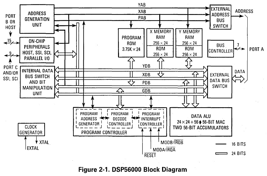
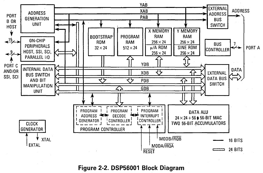
The DSP56000 is a signal processor introduced by Motorola in 1986. The processing unit handles 24-bit numbers at up to 20,5MHz (in the first place). While the DSP56000 was mask-programmed, Motorola produced a variant, the DSP56001, that could be programmed by the user. To do this, the program ROM was replaced by a 512x24 RAM. The remaining bootstrap ROM controls the programming of the chip. In addition, the DSP56001 has a µ-law, an A-law, and a sine table.


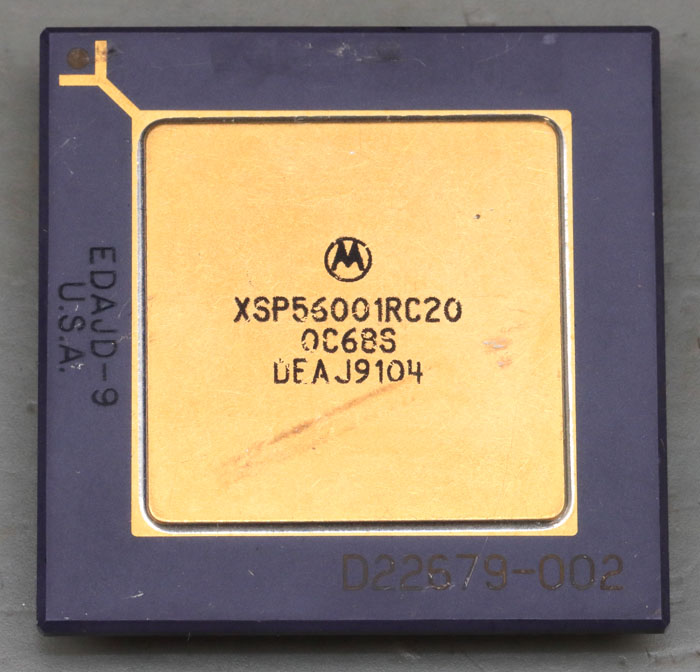
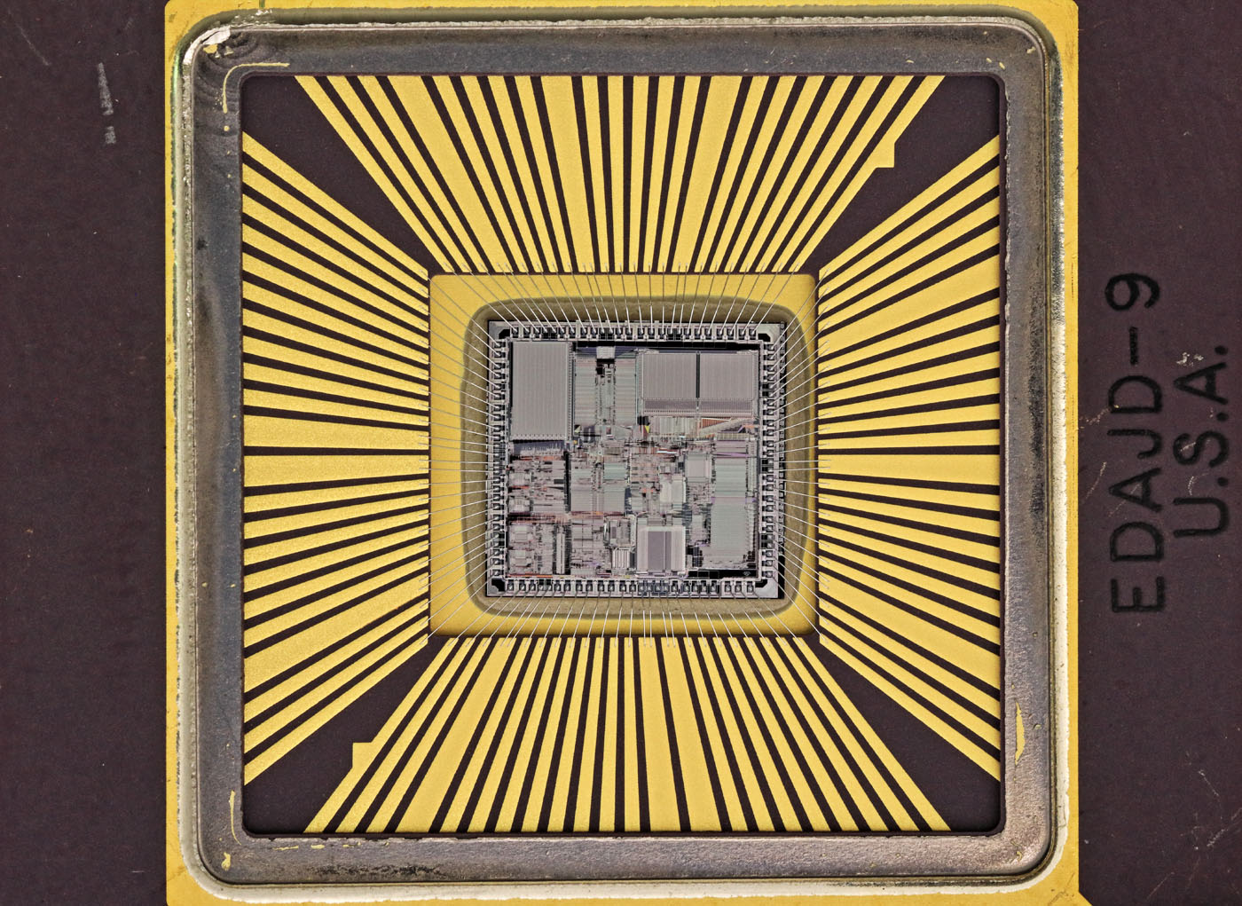
Here you can see an XSP56001RC20. The X indicates that the design has not yet been fully qualified. The abbreviation RC20 indicates the maximum operating clock for which the part is specified. In addition to the 20,5MHz clock, there were variants with 27MHz and 33MHz. As will be shown later, C68S stands for the mask revision used. 9104 could be the datecode, which would then refer to the year 1991.


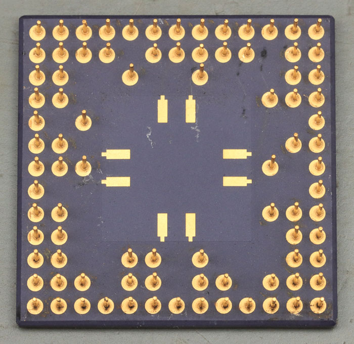
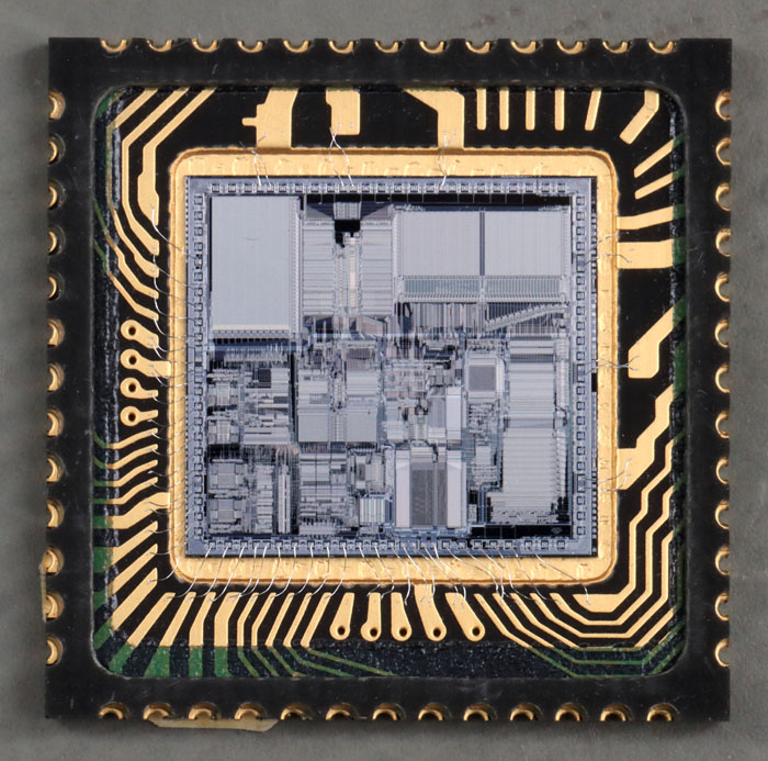
The XSP56001 is housed in a PGA-88 package. Alternatively, QFP-132 packages were also available. The metal surfaces on the underside could be used to mount capacitors, which would then stabilize the supply.


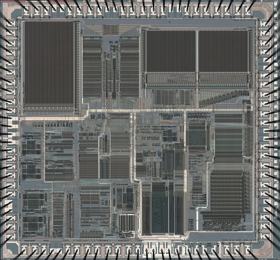
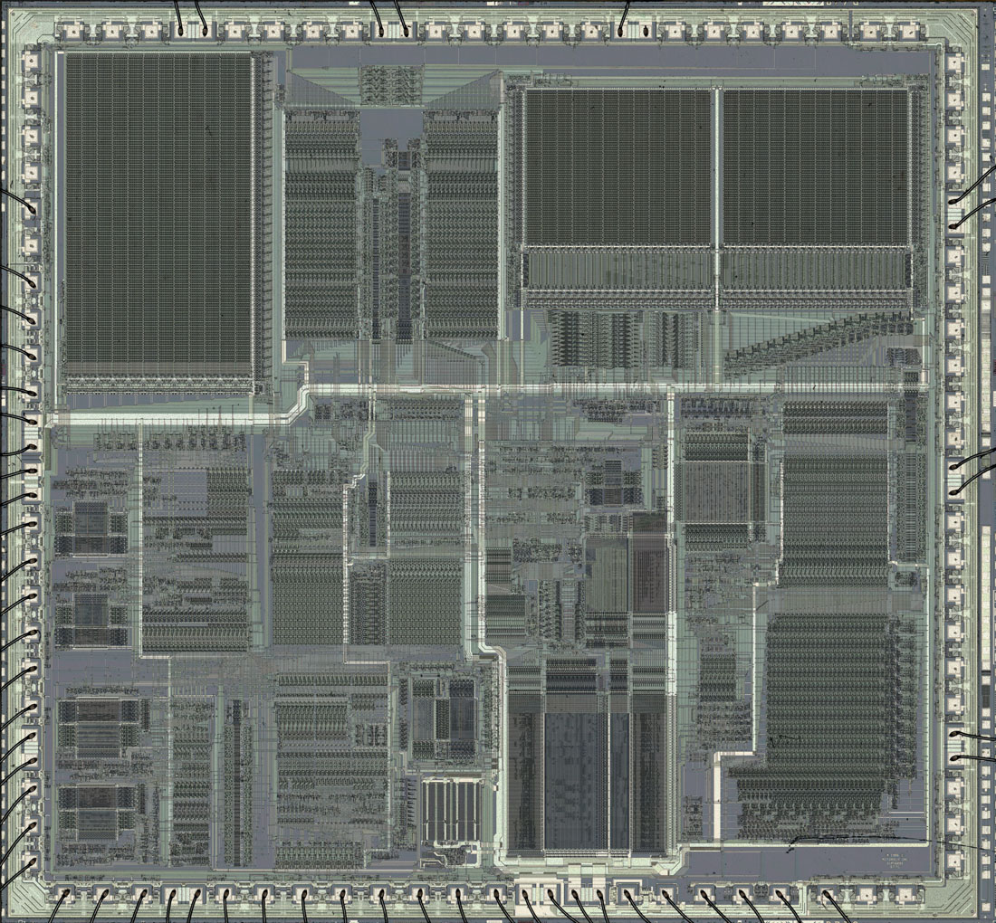
The dimensions of the die are 8,0mm x 7,4mm. The program ROM is located in the upper left corner. The RAM is located in the upper right corner. The slightly smaller memory area at the bottom edge contains the microcode that controls the function blocks of the DSP.

This image is also available in a higher resolution: https://www.richis-lab.de/images/dsp/03x06XL.jpg (51MB)


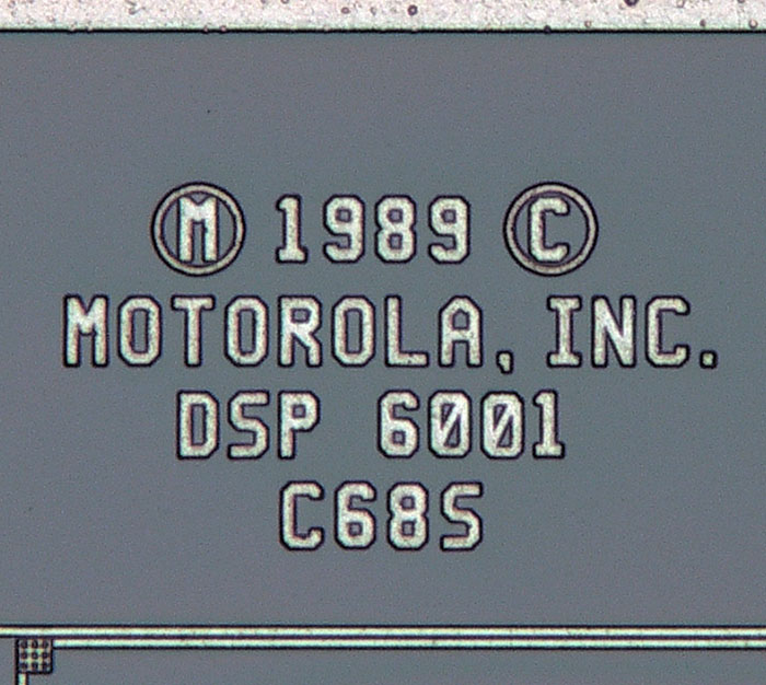
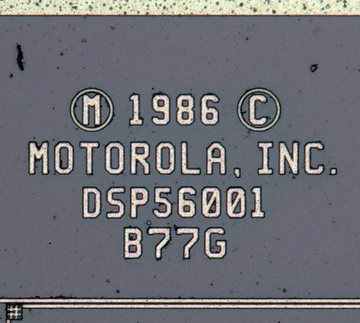
The design dates back to 1989. Interestingly, only the character string DSP 6001 is shown; the number 5 is missing. C68S indicates the mask revision.

A square is depicted in the metal layer in the lower left corner. These squares are often found on the die. They are probably preparations to make it easier to contact these potentials in case of troubleshooting.


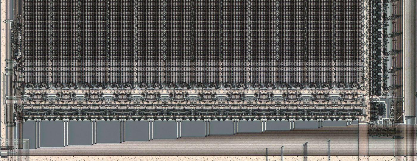
The boundary between the RAM and the boot ROM is clearly visible in the program memory. Apparently, the larger RAM memory cells were used and reconfigured as ROM cells. This approach wastes local silicon area, but allows the RAM's selection and readout circuits to be shared.


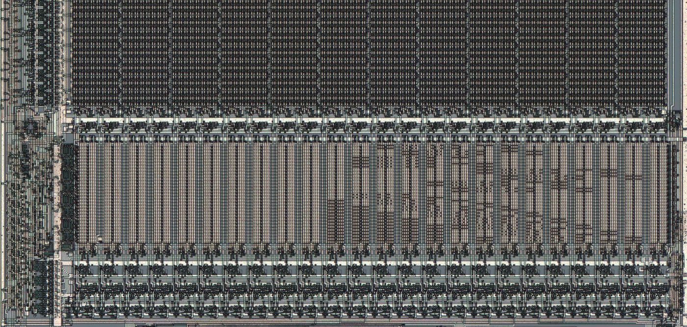
In contrast, optimized ROM areas have been integrated below the working memory. The contents are clearly recognizable.


Here you can see a development part of the DSP56001. The package only has 52 connections, not the 132 contacts that a DSP56001 in a QFP package usually has. Apparently, the data and address bus have been completely omitted.


The dimensions of the die are 11,6mm x 10,7mm. It is thus significantly larger than the C68S revision (8,0mm x 7,4mm). Since the architecture appears to be fundamentally the same, the structure size has apparently been reduced. The 1987 IEEE publication “The Architecture and Applications of the Motorola DSP56000 Digital Signal Processor Family” states that a 1,5µm HCMOS process was used.

This image is also available in a higher resolution: https://www.richis-lab.de/images/dsp/04x01XL.jpg (61MB)


The design dates back to 1986. It is revision B77G. Here, the designation DSP56001 is complete.


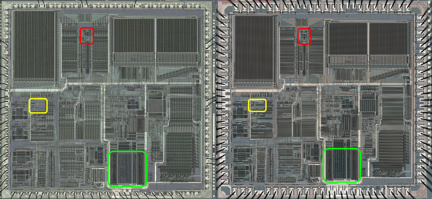
Major changes can be found in three areas. It is not surprising that the microcode has changed (green). A larger circuit section has been added to the left side of the die (yellow).


https://www.richis-lab.de/dsp03.htm

 :-/O
 
The following users thanked this post: RoGeorge, ch_scr, D Straney

Offline NoopyTopic starter

  • Super Contributor
  • ***
  • Posts: 2243
  • Country: de
    • Richis-Lab
Re: Different die pictures
« Reply #451 on: December 01, 2025, 04:33:49 am »


The U820 calculator controller was developed in Dresden at what was then known as the “Arbeitsstelle für Molekularelektronik” (Center for Molecular Electronics). The first prototypes were produced in 1973. Production was moved to Erfurt in 1974. The U821 was then presented at the Leipzig Spring Fair in 1975.

The letter B stands for either production in the second quarter of 1970 or in the first quarter of 1975. Considering the history, this component must have been produced in the first quarter of 1975.


The minirex 73 was the first pocket calculator in the GDR, introduced in 1973. The pocket calculator shown above is on display at the "Technische Sammlung Dresden" (https://tsd.de/). The minirex 73 initially used the TMS0105 from Texas Instruments. This was replaced by the U820 in 1975.


The magazine Radio Fernsehen Elektronik Nr. 23 / 1975 shows the circuit diagram of a typical application with the U820.


The edge length of the die is 5,9 mm. According to a brochure published by the "Zentrum für Mikroelektronik Dresden", the chip was based on an 8µm process. 36mm wafers (~1,5") were used in production. A maximum of 15 U820 chips could be placed on such a wafer.

If you compare the U820 with the TMS0100 family, it becomes clear that it is a 1:1 replica: http://www.datamath.org/Chips/JPEG_TMS0100.htm#Die The only difference is that a whole bunch of small testpads have been added to the die.

This image is also available in a higher resolution: https://www.richis-lab.de/images/calc/04x04XL.jpg (75MB)


https://www.richis-lab.de/calc04.htm


 :-/O


I have also update the U821 with a new and better picture.

This image of the U821 is also available in a higher resolution: https://www.richis-lab.de/images/calc/01x23XL.jpg (114MB)


A comparison of the U820 with the U821 shows that many function blocks have been carried over. The biggest changes are in the upper left corner, but circuits have also been modified in other areas.


https://www.richis-lab.de/calc01.htm#U820

 :-/O
 
The following users thanked this post: RoGeorge, ch_scr, D Straney

Offline NoopyTopic starter

  • Super Contributor
  • ***
  • Posts: 2243
  • Country: de
    • Richis-Lab
Re: Different die pictures
« Reply #452 on: December 04, 2025, 04:06:44 am »


The Texas Instruments TMS0105 is a calculator controller from the TMS0100 family. The datecode refers to the year 1972. The B appears to indicate the revision.


Unfortunately, the die was damaged while doing the decapping. The dimensions are 5,8 mm x 5,9 mm.

This image is also available in a higher resolution: https://www.richis-lab.de/images/calc/05x02XL.jpg (72MB)


There are several character strings in the lower left corner of the die. C 0100A is most likely an internal project designation. To the left of the Texas Instruments logo, the revisions of six masks are shown. The numbers 7/71 on the right-hand side could represent a datecode. The characters 0105A document the variant of the TMS0100. The A suggests that this is a first revision.

It is interesting to note that the characters 05A are located in the mask with the number 3. It remains unclear what function this mask 3 fulfills within the manufacturing process. 6A obviously forms the metal layer. 7 most likely creates the openings in the passivation layer in the area of the bondpads. 1B creates the openings in the initial field oxide at the very beginning of production. This leaves masks 3, 4, and 5. One of these masks defines where the gate oxide will later be located. Another mask forms the openings where the metal layer contacts the substrate. The function of the remaining mask remains unclear. Apparently, mask 3 was used to produce the different variants of the TMS0100 family.


https://www.richis-lab.de/calc05.htm

 :-/O
 
The following users thanked this post: RoGeorge, ch_scr, iMo, D Straney

Offline NoopyTopic starter

  • Super Contributor
  • ***
  • Posts: 2243
  • Country: de
    • Richis-Lab
Re: Different die pictures
« Reply #453 on: December 07, 2025, 04:40:00 am »


The TMS0105 calculator controller was produced with at least two revisions. Revision B has a B in the second line. The version documented here has the letter C in that position.


Unfortunately, the die cannot be removed from the package without causing some damage. Its dimensions are 5,2mm x 4,9mm. Revision C differs significantly from Revision B. It is noticeably smaller and many of the function blocks are also structured differently. According to http://www.datamath.org/Chips/TMS0700.htm, it is the TMS0700, a cost-reduced further development of the TMS0100 family. Apparently, the TMS0700 was then also used in the TMS0105.

This image is also available in a higher resolution: https://www.richis-lab.de/images/calc/06x02XL.jpg (84MB)


Texas Instruments has integrated several character strings in the upper right corner of the die. Unfortunately, this area is damaged. The numbers 0705 are still fully visible. 07 could stand for the TMS0700 family, and 05 could stand for the variant that is functionally similar to the TMS0105. The numbers 00 cannot represent a datecode. Perhaps there was another reference to the TMS0700 family there.

As in Revision B, the numbers 0705 were also displayed here with mask 3. This means that mask 3 also defines the minimally different behavior within the family here.


https://www.richis-lab.de/calc06.htm

 :-/O
 
The following users thanked this post: RoGeorge, ch_scr, D Straney

Offline RoGeorge

  • Super Contributor
  • ***
  • Posts: 7973
  • Country: ro
Re: Different die pictures
« Reply #454 on: December 07, 2025, 05:16:07 am »
Thanks for all the pics so far!  :)
« Last Edit: December 08, 2025, 10:34:54 am by RoGeorge »
 
The following users thanked this post: Noopy

Offline NoopyTopic starter

  • Super Contributor
  • ***
  • Posts: 2243
  • Country: de
    • Richis-Lab
Re: Different die pictures
« Reply #455 on: December 07, 2025, 08:33:19 am »
 8)

Thanks for the feedback! More coming soon...  :-/O :)

Offline marshallh

  • Supporter
  • ****
  • Posts: 1469
  • Country: us
    • retroactive
Re: Different die pictures
« Reply #456 on: January 04, 2026, 09:50:05 pm »
Incredible variety and interesting collection. What a feeling that there could be others like us out in the universe, wondering about what's inside a 1970s calculator chipset  :-+
Verilog tips
BGA soldering intro

11:37 <@ktemkin> c4757p: marshall has transcended communications media
11:37 <@ktemkin> He speaks protocols directly.
 
The following users thanked this post: Noopy

Offline NoopyTopic starter

  • Super Contributor
  • ***
  • Posts: 2243
  • Country: de
    • Richis-Lab
Re: Different die pictures
« Reply #457 on: January 12, 2026, 06:53:40 pm »


The Microchip PIC16F13145 belongs to a family of microcontrollers that operate at a clock speed of 32MHz and contain up to 14kB of Flash-EEPROM and up to 1024B of SRAM.


As a special feature, the PIC16F13145 offers configurable logic blocks, similar to a CPLD. Users can implement time-critical functions there. A so-called “Configurable Logic Block” (CLB) consists of 32 “Basic Logic Elements” (BLE).


Each BLE has four inputs, a lookup table that defines the logical function of this element and a flip-flop.


The package contains a die measuring 2,1mm x 1,9mm.

This image is also available in a higher resolution: https://www.richis-lab.de/images/uC/09x04XL.jpg (20 MB)


Beside the Microchip copyright, the mask revisions of the metal layers are shown. 59F07 appears to be an internal project designation.


The small crosses within the dummy structures are most likely contacts, which of course cannot be easily accessed. However, they make it easier to reach deeper potentials while doing troubleshooting. All you have to do is open the passivation layer and possibly set up a test pad with a FIB. What this might look like is documented with the Philips QU2AGC1 (https://www.richis-lab.de/TBD04.htm). Without the prepared contacts, you would not only have to remove the passivation layer, but also open one or more metal layers in a controlled manner. Any severed wires would then have to be reconnected next to the cut. After that, you can contact the required, deeper potential and lead it upwards in an isolated manner.


After removing the upper layers, you can assign some areas to their functions.

This image is also available in a higher resolution: https://www.richis-lab.de/images/uC/09x07XL.jpg (60MB)


The large, superficially uniform area in the center of the die contains the control logic. In detail, the typical transistor areas of varying sizes can be seen, which are the basis for the individual logic gates.


There are three larger memory areas in total. The block in the lower right corner contains typical SRAM structures (red). The very large block in the upper right corner represents the flash EEPROM (yellow). The block in the lower left corner is somehow special (green). This appears to be a second, smaller EEPROM. These memory cells probably have special properties.


The configurable logic blocks cannot be clearly identified. Due to the size, only one area can actually be considered for this purpose. The structures there are much more uniform than in the control logic, which would be suitable for a configurable logic array.


https://www.richis-lab.de/uC09.htm

 :-/O
 
The following users thanked this post: RoGeorge

Offline NoopyTopic starter

  • Super Contributor
  • ***
  • Posts: 2243
  • Country: de
    • Richis-Lab
Re: Different die pictures
« Reply #458 on: January 25, 2026, 04:08:39 am »


The BK1080 was developed by Beken, a fabless Chinese company. It is a fully integrated FM receiver. The integrated circuit contains the necessary RF circuit components, in which the antenna signal is amplified appropriately and the frequency is downconverted using a PLL oscillator. After digital conversion, the desired frequency is selected and demodulated. Two DACs directly supply two headphones. An integrated voltage converter enables a supply from 2,7V to 5,5V. The BK1080 is controlled via a bus interface.


The datasheet shows a typical application. In addition to the SOP-16 package, the BK1080 is also available in SOP-8, TSSOP-16, QFN-20, and QFN-24 packages. The circuit uses the headphone cable as an antenna.


All functions are integrated on a die with an edge length of 1,1mm. The RF circuitry is obviously located in the upper left corner. The symmetrical structures extending across the entire width below could contain the two DACs and the output amplifiers. The control logic is probably located under the large metal areas in the lower section.

This image is also available in higher resolution: https://www.richis-lab.de/images/radio/02x04XL.jpg (12MB)


The structures are too display them in all details.


https://www.richis-lab.de/radio02.htm

 :-/O
 
The following users thanked this post: Vgkid, RoGeorge, D Straney

Offline NoopyTopic starter

  • Super Contributor
  • ***
  • Posts: 2243
  • Country: de
    • Richis-Lab
Re: Different die pictures
« Reply #459 on: Yesterday at 04:09:04 am »


The RDA5807 is a fully integrated FM receiver from the Chinese company RDA Micro. Following a takeover by Tsinghua Unigroup, this eventually led to the creation of the company UNISOC. The datasheet contains a block diagram similar to that of the BK1080. The functional blocks are simply shown in greater detail (with fewer pixels  ;D). The RDA5807 also extracts RDS data from the signal.


Measuring 1,1mm x 0,8mm the die is slightly smaller than that of the BK1080. An inductor is located on the right-hand side, indicating that this is where the RF part of the circuit is located. The rest is covered by a fairly homogeneous grid structure.

This image is also available in a higher resolution: https://www.richis-lab.de/images/radio/03x03XL.jpg (56MB)


The structures are too small to be completely resolved.


https://www.richis-lab.de/radio03.htm

 :-/O
 
The following users thanked this post: RoGeorge, iMo, D Straney

Offline D Straney

  • Frequent Contributor
  • **
  • Posts: 360
  • Country: us
Re: Different die pictures
« Reply #460 on: Yesterday at 04:46:56 am »
That's kind of disappointing when most of the circuitry is covered by metal (always enjoy the inductors though!).  The MCU in an automotive transmission controller I opened recently also had the densest metal fill I'd ever seen - the only things visible were a few power traces on the top layer.  Zoomed section below:
 
The following users thanked this post: RoGeorge

Offline NoopyTopic starter

  • Super Contributor
  • ***
  • Posts: 2243
  • Country: de
    • Richis-Lab
Re: Different die pictures
« Reply #461 on: Yesterday at 04:50:25 am »
 :-+

Sometimes I strip everything with HF to see a little bit more. Perhaps I should do that with these two FM receivers...

Offline iMo

  • Super Contributor
  • ***
  • Posts: 6413
  • Country: sm
Re: Different die pictures
« Reply #462 on: Yesterday at 09:20:40 am »
I wonder for what the aprox 0.5nH large inductor on the FM receiver chip is good for. Perhaps for a PLL for the local oscillator?
Readers discretion is advised..
 

Offline NoopyTopic starter

  • Super Contributor
  • ***
  • Posts: 2243
  • Country: de
    • Richis-Lab
Re: Different die pictures
« Reply #463 on: Yesterday at 03:06:44 pm »
I don´t know...  :-// I don´t have a lot of experience with modern RF circuits on silicon.


Share me

Digg  Facebook  SlashDot  Delicious  Technorati  Twitter  Google  Yahoo
Smf