Author Topic: Different die pictures  (Read 90332 times)

0 Members and 1 Guest are viewing this topic.

Offline TimNJ

  • Super Contributor
  • ***
  • Posts: 1661
  • Country: us
Re: Different die pictures
« Reply #175 on: December 25, 2021, 03:23:53 pm »

Is the STP3NB100FP (https://www.richis-lab.de/FET15.htm) already a superjunction MOSFET? Not sure...


As far as I know, ST's super-junction types are under the name MDMesh. This one is PowerMesh, so my vote is that it's not super-junction.
 

Offline NoopyTopic starter

  • Super Contributor
  • ***
  • Posts: 1749
  • Country: de
    • Richis-Lab
Re: Different die pictures
« Reply #176 on: January 10, 2022, 05:51:13 am »


The Intersil ICL8038 is a Precision Waveform Generator: 0,001Hz - 300kHz square wave, triangle and sine wave output with a duty cycle of 2%-98%. Supplied with 30V the chip can generate a signal with 28Vpp.


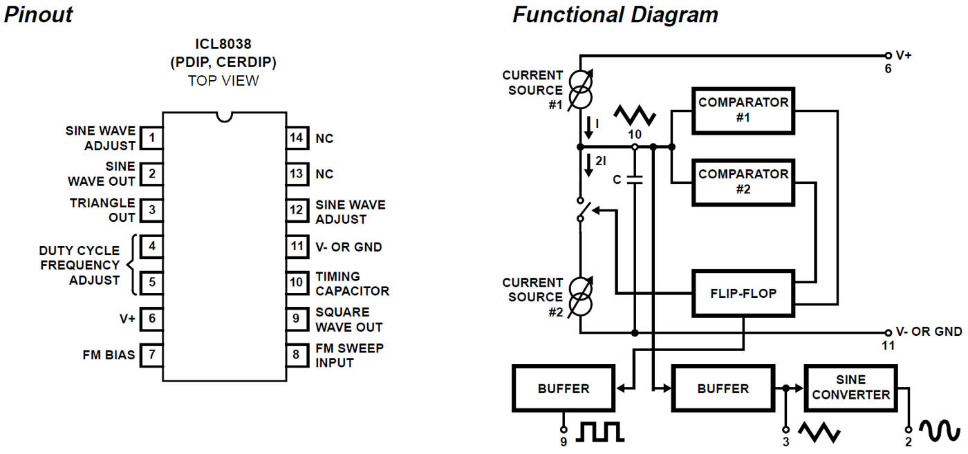
The datasheet contains a block diagram. There are two current sources, one charging, one discharging a external capacitor. Since the discharging part sinks twice the current of the charging source you just have to switch the sink to get +/-I. At the capacitor you get the triangle wave. A sine shaper converts the triangle into a sine wave. Two comparators and a flip-flop are managing the current switching to get the oscillation we want. At a second output of the flip-flop there is the rectangle wave.


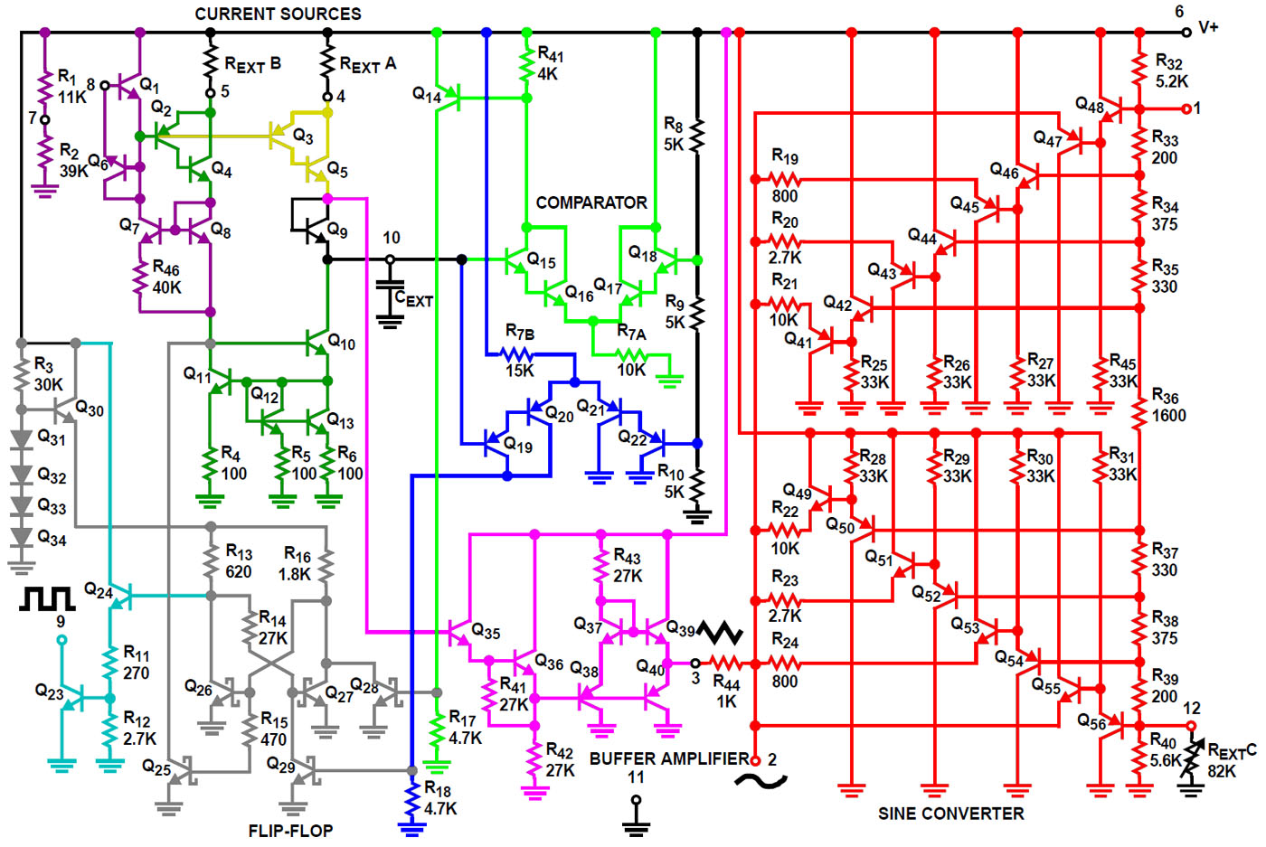
In addition the datasheet contains a schematic (colored by me).
The current source (yellow) is a Sziklai circuit. The current sink (dark green) is based on a current source like the former one. It is transformed into a current sink with a current mirror that also doubles the current. Both current sources are based on the same reference (purple). The currents of the current sources are determined by the external resistors RextA and RextB. With these resistors and the integration capacitor Cext you can set the working frequency. The frequency can be varied through pin 8, which manipulates the reference circuit and so the current sources. Behind pin 7 there is a voltage divider. If you don´t want to adjust the frequency you just have to connect pin 7 and pin 8.

The triangle signal at the integration capacitor is tapped above the transistor Q9 which is connected as a diode. In the buffer amplifier for the triangle signal (pink) there is a Darlington circuit in the first place (Q35/Q36). It is followed by an interesting output stage whose main component is the transistor Q40. The potential at pin 3 is determined by the base-emitter junctions Q9 / Q35 / Q36 / Q40. Thanks to the transistor Q9, the potential at pin 3 is at the same level as the potential of the integration capacitor. Through Q9 / Q35 / Q36 / Q38 / Q37 the base of the transistor Q39 is slightly higher and thus provides some pull-up / bias current. According to the datasheet, the output stage can draw up to 25mA. A diagram shows that the current delivery capability is much more limited. The signal oscillates around half the supply voltage. If one uses a balanced supply, the average value settles at 0V.

To generate a sinusoidal signal. The triangle wave is fed with a relatively high impedance (R44) into a circuit that represents a voltage dependent impedance (red). As the level of the triangular wave increases, the load increases and more voltage drops across R44, reducing the rise of the voltage at pin 2. This results in the desired sinusoidal signal, more precisely an approximation. The voltage dependent impedance is generated with a large symmetrical circuit. The PNP transistors Q41, Q43, Q45 and Q47 become conductive one after the other as the voltage rises and draw different currents depending on their emitter resistances. Behind each transistor a second transistor determines the voltage the stage kicks in. These transistors are connected to a large voltage divider at the right edge. For the low level part of the signal, the same circuit is built in a complementary way in the lower part of the schematic. Here the NPN transistors Q49, Q51, Q53 and Q55 supply a current that increases as the voltage drops. With the help of pin 1 and 12 it is possible to adjust the circuit so that the distortion of the sinusoidal signal gets below 0.5%. Without the adjustment the typical distortion of the worst case ICL8038CC is 2,0%.

The two comparators are connected to the integration capacitor (light green/blue). The resistors R8, R9 and R10 determine the switching points of the comparators. The output signal of the upper comparator is inverted by transistor Q14. The Flip-Flop (grey) is built with Schottky transistors. These transistors have a Schottky diode between base and collector which prevents the transistor from being driven into saturation so it can be switched off faster. The Flip-Flop has its own small voltage regulator (Q30-Q34). The current sink (dark green) is switched off by the output of the flip-flop draining the current in the reference path of the current mirror. The buffer amplifier for the square wave signal provides an open collector output (cyan).


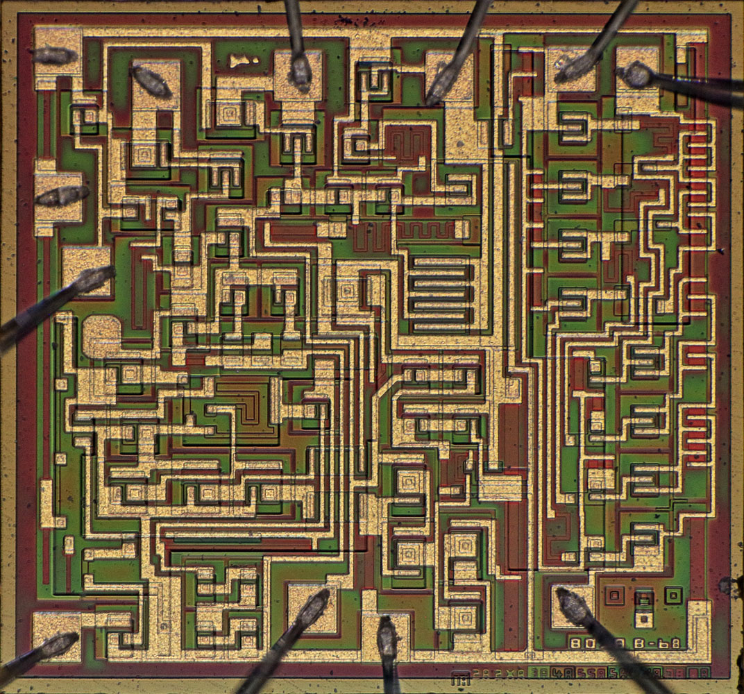
The die is 1,9mm x 1,8mm.


Intersil


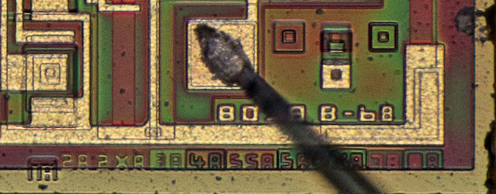
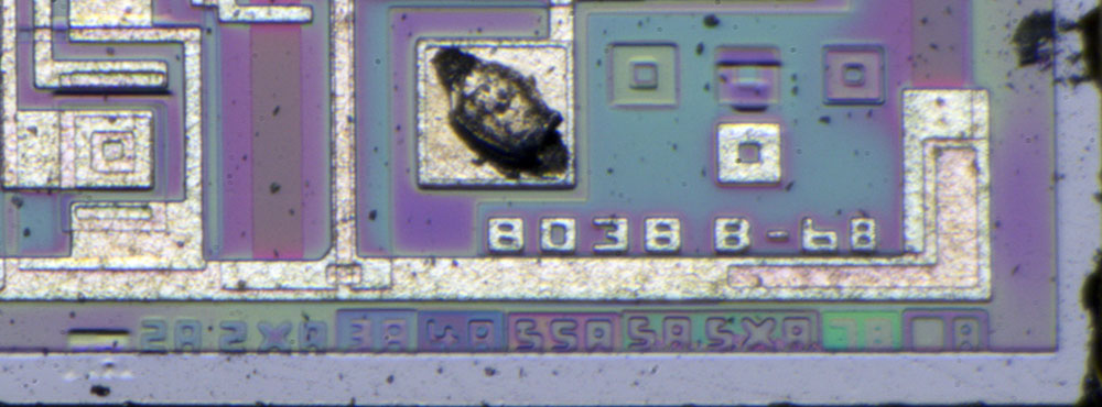
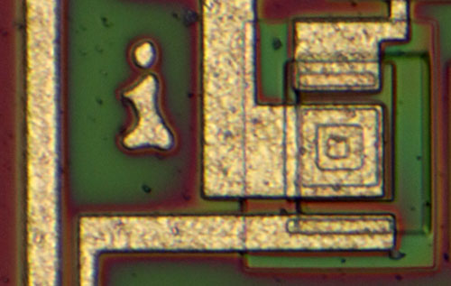
In the lower right corner we have the mask revisions. The revision of the metal layer (6B) is moved to the part name. The B at the end of the name is probably the revision of the whole design.
This "mi" thing on the left could be a signature...  :-//


On the left edge of the die we have the voltage divider for the current source reference.
The upper part (red) should have 11k while the lower part (green/cyan) should have 39k. It looks like the lower part can be tuned.  :-/O The cyan part probably contributes a lower resistance which can be connected by some vias. The lower contact of the green resistor looks like it can be moved.


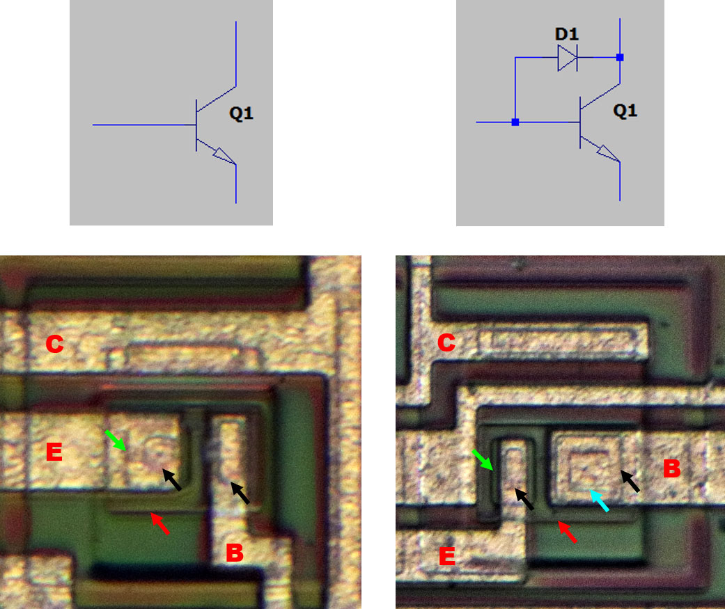
Here you can see the difference between a normal transistor (left) and a Schottky transistor (right). In both transistors you can see the edges of the base (red) and the emitter (green) areas. You can recognize the contact areas too (black). The Schottky transistor is equipped with a very big base contact which has an additional edge (cyan). That is probably a hole in the base area through which the metal makes contact with the slightly n-doped collector. At this contact you get a Schottky diode.


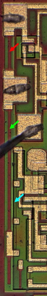
In comparison with the rectangular output transistor (green) the triangle output transistor (red) is quite big. That´s because it´s a PNP and it works in linear mode with a higher power dissipation than the rectangle output that just switches on and off.


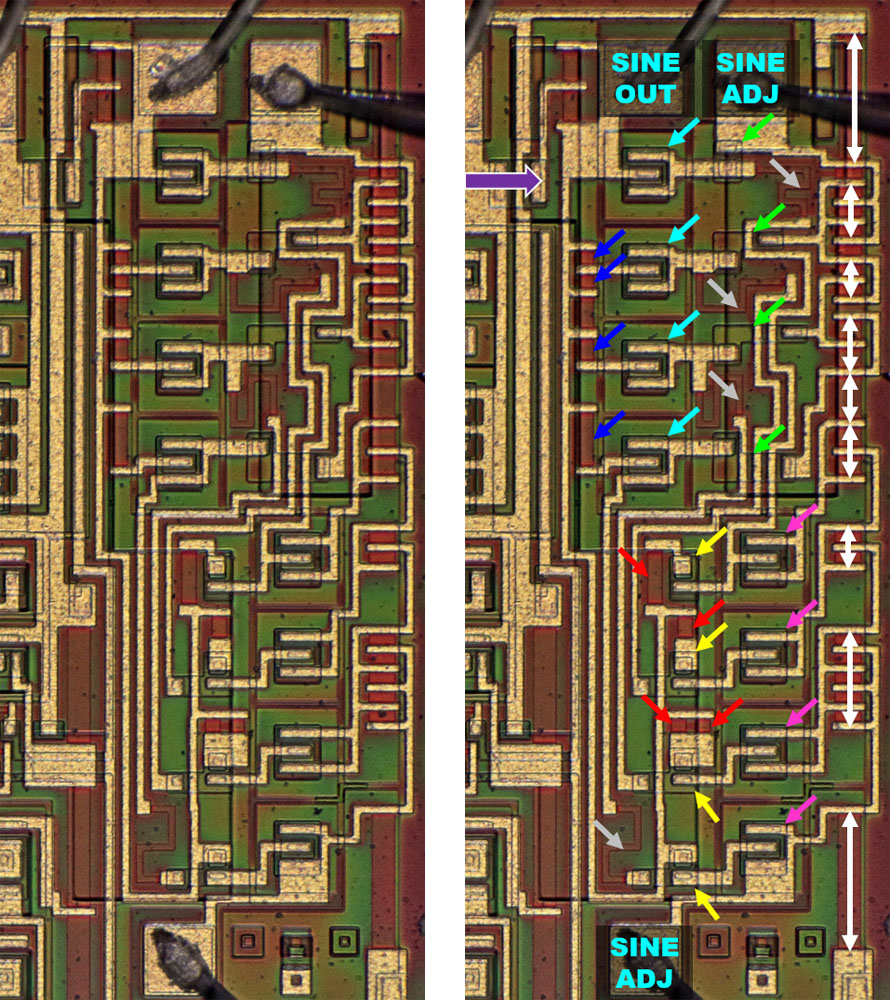
The sine shaper occupies a relatively large area on the right side of the die. In the upper half there are the PNP transistors, which represent the variable impedance to ground (cyan). To the left of them you can see the emitter resistors (blue). The different sizes are easy to recognize. For the lowest resistor value (800Ω), two elements were connected in parallel. Right of the load transistors there are the transistors that determine the voltage at which the stage kicks in (green). Some of the base areas had been extended to accomplish the wiring with just one metal layer.

In the lower area, the smaller NPN transistors (yellow) with their emitter resistors (red) are located on the left as a load. The less efficient and therefore larger PNP transistors, which determine the voltage the stage kicks in, are right of the load transistors (pink).

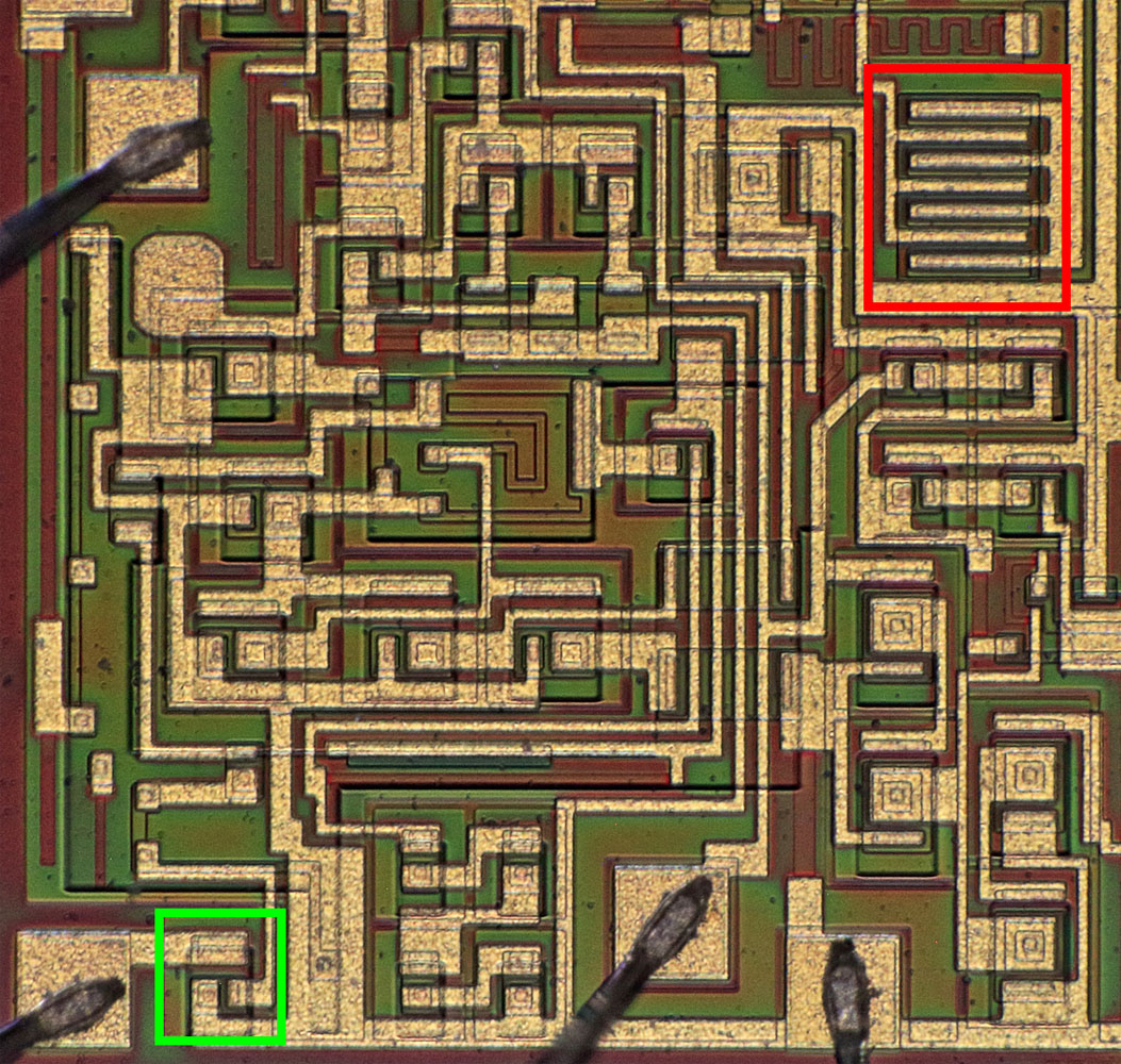
At the right edge of the die the resistors of the large voltage divider are integrated (white). To get the smaller values some of the areas are connected in parallel.


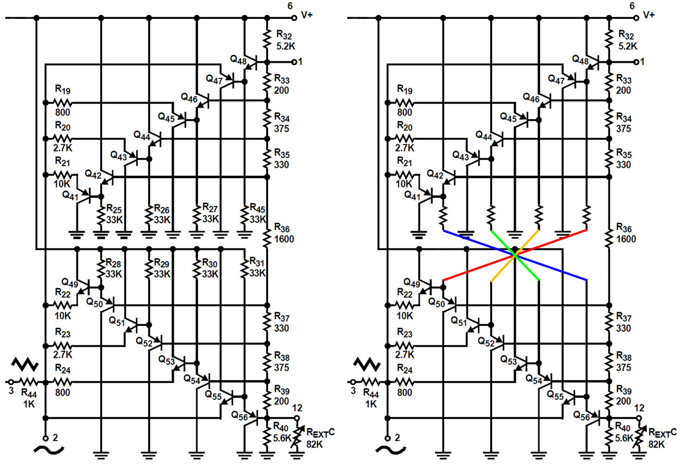
A closer look reveals that the transistors setting the onset voltage are not connected to the ground and supply potential as shown in the datasheet. Instead the opposite stages are cross-connected. This circuit consumes less area on the die. Perhaps it gives you a nicer sine wave too.  :-// Would have to simulate the circuits...


https://www.richis-lab.de/gen02.htm

 :-/O
« Last Edit: January 10, 2022, 08:44:23 pm by Noopy »
 
The following users thanked this post: SeanB, doktor pyta, RoGeorge, bsw_m, ch_scr, Lacibácsi

Offline NoopyTopic starter

  • Super Contributor
  • ***
  • Posts: 1749
  • Country: de
    • Richis-Lab
Re: Different die pictures
« Reply #177 on: January 14, 2022, 05:19:54 am »


In the GDR the NEC µPD7220 (https://www.richis-lab.de/GraKa02.htm) respectively the Intel D82720 (https://www.richis-lab.de/GraKa03.htm) was copied and named U82720. It was built by "Mikroelektronik Karl Marx".

DC02 is the slowest version (2MHz). There was a DC03 (3MHz) and a DC04 (4MHz). With these clocks the U82720 is a little slower than the NEC and the Intel.

X3 stands for March 1989.


The die was placed on a quite massive metal carrier that probably has to spread the power dissipation.


The U82720 design is exactly the same as the µPD7220 design (and the D82720 design). There are just very few differences.

With 7mm x 6,8mm the die is noticeable bigger than the die of the µPD7220 (5,6mm x 5,6mm). On the IEEE International Solid-State Circuits Conference 1981 the µPD7220 was introduced with an edge length of 7mm. The website www.oguchi-rd.com states that the first design was built with a 4µm process and the final product was built with a 3µm process. Combining this information we can assume that the U82720 was built with a 4µm process.


There are even the free areas where the NEC and the Intel logo were placed.


It seems ground connection was a critical point. The µPD7220 had two contacts at the right edge of the die. The later µPD7220A was smaller but nevertheless had three contacts. The U82720 has three contacts on the right edge and an additional ground contact on the left edge.


The U82720 uses a different and especially bigger bias generator. Perhaps the leakage current of the U82720 was higher.


The output stages look the same as in the µPD7220.


The input stages look different in the U82720, in the µPD7220, in the D82720 and in the µPD7220A. But it looks like it´s always a grounded Gate NMOS protecting the circuit.


https://www.richis-lab.de/GraKa04.htm

 :-/O
 
The following users thanked this post: SeanB, RoGeorge

Offline NoopyTopic starter

  • Super Contributor
  • ***
  • Posts: 1749
  • Country: de
    • Richis-Lab
Re: Different die pictures
« Reply #178 on: January 29, 2022, 09:31:43 pm »
An interesting analysis would be a silicon capacitor ( https://www.mouser.sk/Passive-Components/Capacitors/Silicon-RF-Capacitors-Thin-Film/_/N-5g95 ). Some seem to have far more advanced structures on them :)

Done! :)


Murata 935174732547, a 47nF 30V silicon capacitor from the ATSC series. It is integrated in a 0505 package (1.32mm x 1.32mm) with a height of just 0.25mm. The ATSC capacitors are to be connected with bondwires but there are SMT packages too.

Compared to a conventional MLCC a silicon capacitor is much more expensive. Mouser states a 1kpc price of 4.16€ excl. VAT. But Silicon capacitors offer several advantages over conventional MLCCs:
  • One important point is the high temperature resistance. The ATSC series is approved up to 200°C. Up to 250°C is possible (XTSC series).
  • Over the operating temperature range and the operating voltage range, the properties of the capacitors hardly change. Aging effects are also negligible.
  • The special structure offers high capacitance in the smallest possible space. The largest model in the ATSC series is a 1616 package (4.07mm x 4.07mm x 0.25mm) offering 1µF 30V.
  • ESL and ESR are very low too so they are well suited for high frequency applications. The XBSC model series guarantees 100pH/300mΩ and is specified up to 100GHz.
  • The insulation resistance is in the GΩ range.

You can clearly see that the two bondpads at the top edge are connected to the top metal layer and the two bondpads at the bottom edge are connected to the lower metal layer. Most of the area is filled with the special capacitor structures.


Murata Assembly Note states that EJ05055473 is the "die name" whatever that means.


On the Murata website there is the document "Silicon Capacitors with extremely high stability and reliability ideal for high temperature applications", which describes in detail how silicon capacitors are built. The technology is similar to the deep trench MOSFETs. On the substrate there is an array of cylindrical holes that are very deep in relation to their diameter. A heavily n-doped layer applied over the entire surface is the bottom electrode (blue). It is followed by the dielectric (green) and another heavily n-doped layer that is the top electrode (red). The holes greatly increase the effective area. In combination with the small distance between the holes, this results in very high capacitance.

According to the document above you can achieve a capacitance densities of up to 550nF/mm² if you use a dielectric with a high dielectric constant (Vmax=11V). Murata states that silicon capacitors with voltage strengths up to 450V are available. The capacitance density decreases accordingly. 6nF/mm² are documented for 150V.


The Murata website illustrates that their capacitors not just work with the classic trenches, but also uses 3D structures. The enlarged surface makes it possible to further increase the capacitance density.


The area consists of 210 small areas. Apparently the upper metal layer contacts the lower electrodes of each capacitor area through short vertical strips of the lower metal layer. The lower metal layer contacts the upper electrode via a large area. The pattern in this areas is created by the trenches that increase the effective surface area.

On the left and the right side there are two big substrate contacts. There are silicon capacitors that are constructed with three electrodes, what further increases the capacity. However, it seems unlikely that this is the case here. Dividing the capacitance into 210 small areas reduces the capacity, but it also reduces ESL and ESR. It wouldn´t make sense to connect a third electrode just via two simple lateral contacts, which would again worsen ESL and ESR. Probably the lateral contact  ensures that the substrate is at a defined potential.


https://www.richis-lab.de/SiCAP01.htm

 :-/O
 
The following users thanked this post: SeanB, daqq, doktor pyta, RoGeorge, ch_scr, MegaVolt

Offline daqq

  • Super Contributor
  • ***
  • Posts: 2302
  • Country: sk
    • My site
Re: Different die pictures
« Reply #179 on: January 29, 2022, 09:40:39 pm »
Thanks! Pretty fascinating structure.

One thing that came to mind: This is a pretty high capacitance per mm2. How thick is the useful structure? Assuming infinite budget and shaving the back end of the chip to nothing, how much capacitance could you theoretically pack into one mm3 ?
Believe it or not, pointy haired people do exist!
+++Divide By Cucumber Error. Please Reinstall Universe And Reboot +++
 

Offline NoopyTopic starter

  • Super Contributor
  • ***
  • Posts: 1749
  • Country: de
    • Richis-Lab
Re: Different die pictures
« Reply #180 on: January 29, 2022, 10:00:07 pm »
The ATSC capacitors are 250µm high. Murata offers capacitors with a height of 100µm.

I have heard that the maximum depth-to-diameter-factor of such trenches is round about 60. It seems like the diameter of the trenches is smaller than 1µm.
So let´s assume a height of 50µm would be possible. That would supply us with a capacitance of 11µF/mm³! Nice!  8)
« Last Edit: January 30, 2022, 05:31:26 am by Noopy »
 

Offline T3sl4co1l

  • Super Contributor
  • ***
  • Posts: 21729
  • Country: us
  • Expert, Analog Electronics, PCB Layout, EMC
    • Seven Transistor Labs
Re: Different die pictures
« Reply #181 on: January 30, 2022, 02:43:33 pm »
Dielectric is just silica, right?  Or do they have other types available too (the comment about higher k seems to suggest so)?  And in that case, I wonder how they do it; atomic layer deposition or something?  If they're doing that, with like the high-K gate oxide (HfO2) they're doing on other processes, that'd be fascinating.

(And, I do see a few papers showing HfO2, etc. can be deposited in this way.  Nice.)

Tim
Seven Transistor Labs, LLC
Electronic design, from concept to prototype.
Bringing a project to life?  Send me a message!
 

Offline NoopyTopic starter

  • Super Contributor
  • ***
  • Posts: 1749
  • Country: de
    • Richis-Lab
Re: Different die pictures
« Reply #182 on: January 30, 2022, 03:22:21 pm »
The paper I mentioned states that the 550nF/mm² are achieved with high k dielectrics:

Quote
Obviously this huge capacitance density increase is achievable thanks to higher k-dielectric layers and to the ALD (atomic layer deposition ) enabling excellent step coverage of the deposited layer [2]. 

Semiconductor manufacturing was always a fancy mixture of physics and chemistry but the freaky processes of today in combination with the huge amount of elements involved that is a kind of magic.  :-/O

Offline T3sl4co1l

  • Super Contributor
  • ***
  • Posts: 21729
  • Country: us
  • Expert, Analog Electronics, PCB Layout, EMC
    • Seven Transistor Labs
Re: Different die pictures
« Reply #183 on: January 30, 2022, 05:44:49 pm »
Aha, figured it would have to be. :D

Yeah, the processes, what we can do these days, is incredible!

Tim
Seven Transistor Labs, LLC
Electronic design, from concept to prototype.
Bringing a project to life?  Send me a message!
 

Offline NoopyTopic starter

  • Super Contributor
  • ***
  • Posts: 1749
  • Country: de
    • Richis-Lab
Re: Different die pictures
« Reply #184 on: March 03, 2022, 08:41:15 pm »


Let´s take a look into a NFC credit card.


Some paint stripper and the credit card dismantels into three plastic sheets. The material swells up a little.


The chip of the card is fixed in the upper sheet.

The NFC antenna is located in the middle. The three windings are located so stamping the numbers and characters doesn´t damage the wire.


The antenna winding forms two meander. In this area two small plates connect the chip with the antenna. I assume the meander are just for tolerance compensation.


Under the electrodes of the card there is the chip connected with seven bondwires. Five wires connect the electrodes and two wires contact the antenna through kind of a frame structure.


The die is 2,7mm x 1,9mm x 0,15mm. The whole area is covered with a uniform metal structure. On the left side there are four testpads and nine bondpads. In this area the structures are a little thicker. I assume there are protection structures, power supply and the transceiver.


Unfortunately the structures are a little small. It looks like 041, NXP and 2016. But I´m not sure with the last two.


A closer look reveals that the stripes of the metal layer are connected with the lower structures in a regular way. Under the metal layer you can see another layer. It consists of parallel stripes too but they are rotated by 90°.

This is a common protective feature. The uniformly structured metal layer prevents simple optical analysis of the circuit. Since the individual lines are electrically connected to the circuit, it is not possible to remove the metal layer without destroying the circuit. It is possible to create small openings and reconnect the leads around them, but this process is quite complex and time-consuming, especially if you want to contact multiple potentials.


https://www.richis-lab.de/transponder03.htm

 :-/O
 
The following users thanked this post: SeanB, RoGeorge

Offline T3sl4co1l

  • Super Contributor
  • ***
  • Posts: 21729
  • Country: us
  • Expert, Analog Electronics, PCB Layout, EMC
    • Seven Transistor Labs
Re: Different die pictures
« Reply #185 on: March 03, 2022, 09:22:37 pm »
I wonder if they also get some bypass capacitance from the array of metal stripes (and probably layers too?)?  Should be handy for the self-powered NRC mode. :)

Tim
Seven Transistor Labs, LLC
Electronic design, from concept to prototype.
Bringing a project to life?  Send me a message!
 

Offline NoopyTopic starter

  • Super Contributor
  • ***
  • Posts: 1749
  • Country: de
    • Richis-Lab
Re: Different die pictures
« Reply #186 on: March 04, 2022, 04:19:02 am »
That´s definitely possible!  :-+

Offline NoopyTopic starter

  • Super Contributor
  • ***
  • Posts: 1749
  • Country: de
    • Richis-Lab
Re: Different die pictures
« Reply #187 on: March 17, 2022, 10:33:22 am »


The Sega Virtua Processor (SVP) is a DSP Sega integrated in one game cartridge of the Mega Drive system. A normal game cartridge contains just a ROM with the game data. For the game Virtua Racing Sega integrated the SVP to support the console by rendering polygons.

The SVP is marked with the SEGA logo and the numbers 315-5750. The package is a TQFP with 120 pins. Beside the SVP there is the game ROM (IC2, right side) and a 128kB RAM (IC3, left side).

You can find a lot of information about the functionality of the SVP here at Github: https://github.com/jdesiloniz/svpdev


Internet says the SVP is a rebranded Samsung SSP1601 DSP. Since the SSP1601 sits in a package with 68 pins the SVP is clearly not just a rebranded SSP1601.


The die of the SVP is 8,0mm x 7,6mm. Here you can find a higher resolution (16.312 x 15.632, 55MB): https://www.richis-lab.de/images/GraKa_S3/05x02xlarge.jpg


There is a Samsung copyright dating back to 1993.

SEGA160FS seems to be the internal naming of the chip. "160" because of the SSP1601?

It looks like this name is in two different masks, perhaps two metal layers or a metal layer and a via mask. As we will see later on it looks like the SVP is based on a standard design that can be used for different applications.


Some test structures...


The package has 4*40 pins. The die has 2*58 and 2*56 bondpads. 42, 44, 44 and 46 bondpads were contacted with bondwires. Some of the supply pins were connected with more than one bondpad.


With the help of the layout you can identify the role of most of the pins.


The supply bondpads are connected to the die more heavily than the normal I/Os. Some are connected to the frame structure conducting supply around the edges (95, 92). Some supply bondpads conduct current into the middle of the die.


There are some non-contacted bondpads. These bondpads are not connected to the rest of the circuit either. In the same way, there are also unused I/O structures. This makes me assume that the die is based on a rather universal design.

The active bondpads are connected to the frame structure with two wide lines and one narrow line. The two wide outer frames contain the output drivers. Most likely, these areas serve as protection structures for inputs too.

Further inside the chip there run additional supply lines within which two logic lines are integrated. It is noticeable that there are only two variants of these logic structures. The right variant is very simple and has only one control line. The left logic is more complex and is connected with more lines. Looking at the use of the individual I/Os one can speculate that the larger variant is kind of a latch for synchronized reading and buffering the logical state of the pin.


The RAM and ROM address lines for example are controlled by the simple outputs. The pins that have to read data lines on the other hand are equipped with the extended logic structures (white diamonds).

Apart from the supply lines, deviating structures can only be found in the area of the clock conditioning. There we have two lines connecting the circuit directly with two bondpads (green).


...
 
The following users thanked this post: SeanB, RoGeorge

Offline NoopyTopic starter

  • Super Contributor
  • ***
  • Posts: 1749
  • Country: de
    • Richis-Lab
Re: Different die pictures
« Reply #188 on: March 17, 2022, 10:34:28 am »


The different structures of the various function blocks quickly give a rough overview of the structure of the SVP. The I/Os extend over all four edges (cyan). At the upper edge there is a small circuit (green), where the device probably generates its clock.

The DSP can clearly be identified because of its different but in itself again regular structures (red). Directly connected to the DSP is a large memory with the typical regular structure (pink). As will be shown, there are two SRAM areas with 256*16Bit of memory each.

In the upper right corner of the die there is a ROM (yellow). It consists of two areas with 1kB each. In this memory there are for example basic instructions. In the upper left corner there is another SRAM with a capacity of 2kB (blue).

In the free area between the large function blocks there are gatearray structures (white). This gatearray contains the logic that connects the individual function blocks with each other, with the external components and the game console. The large area suggests that there are quite some function integrated into the gatearray.


In some areas of the gatearray you can see the standard cell structure interconnected with probably two metal layers.


The area at the top edge probably provides the clock for the SVP. It contains relatively large elements. The circuit is directly and exclusively connected to an external capacitor via two pins. A special clock feed from the game console is not visible. It is quite conceivable that this is an oscillator, via which the SVP generates its own working clock. Perhaps the DSP could even be overclocked by changing the value of the external capacitor or the surrounding components.


The ROM in the upper right corner is considerably smaller than the RAM. That´s because such a mask programmed ROM generally consists of just one Transistor while a SRAM generally needs six transistors.


The structures are very small, but you can estimate the memory size. The structure is similar to the MK37092 mask ROM (https://www.richis-lab.de/ROM02.htm) although here it seems that the line selection takes place at the side and the data is outputed at the lower edge.

Between the two memory blocks several control signals are fed from below (white). From there 4+2 control signals each lead to the left and to the right memory block (red). On the inside of each memory block 64 control signals are generated and a single line is activated (red). Each of the two memory blocks feeds eight data lines (yellow) independently of the other area. 12 control signals (green) allow to select one of 18 columns to each of the data lines. In total, this results in a 2kB memory.


The SRAM in the upper left corner of the die consumes a lot of area. At the upper edge of the memory area there is a 32Bit wide data interface (green). Four control lines connect each data line to one of eight columns of the memory area (blue/cyan). Seven control lines arrive from the right side. At this edge there is a circuit that selects one of the 64 rows. Altogether this results in a memory size of 2kB.

In the row selection, you can just make out the differently placed vias that allow addressing a single row. The individual memory cells can only be guessed.


Here you can see the DSP itself. There is also a high resolution picture (4.416 x 4.572, 4MB): https://www.richis-lab.de/images/GraKa_S3/05x23xlarge.jpg


The datasheet of the SSP1601 states that the DSP itself is 3,6mm x 2,4mm. That is exactly the size we see in the SVP.


You can´t identify every part of the DSP but there is a 32Bit-ALU and the 16*16-Mulitplier.

It looks like the SRAM has the same size as stated in the SSP1601 datasheet.

The not marked areas could contain some or all of the other circuits mentioned in the block diagram.


The ALU with 32 elements.


The 16*16 multiplier has a nice uniform square structure.


The structures of the DSP SRAM are as small as the structures of the SRAM in the upper left corner but it is still big enough to determine the size.


Each of the two SRAM blocks is divided into two areas. Between the areas is the the line selection circuit (yellow). You can see 32 similar small circuits. They probably control 64 lines. It´s very likely the memory density is the same as in the other SRAM block.  The control lines for the row selection run from the upper right corner of the memory down the right side and to the row selection circuit. Each of the four memory areas contains 32 columns (cyan). These columns are merged into four times 8 data lines (green). This results in a total of 1kB of memory.


https://www.richis-lab.de/GraKa05.htm

 :-+
« Last Edit: March 20, 2022, 08:35:04 am by Noopy »
 
The following users thanked this post: SeanB

Offline NoopyTopic starter

  • Super Contributor
  • ***
  • Posts: 1749
  • Country: de
    • Richis-Lab
Re: Different die pictures
« Reply #189 on: March 20, 2022, 05:31:29 am »
A small update:
I was wrong with counting!
The SRAM in the upper left corner of the die is 2kB. That´s interesting because with the correction this SRAM is more dense than the SRAM of the DSP. Perhaps the they used a different cell structure for the DSP.  :-//

Pictures have been updated...
« Last Edit: March 20, 2022, 07:20:50 am by Noopy »
 

Offline NoopyTopic starter

  • Super Contributor
  • ***
  • Posts: 1749
  • Country: de
    • Richis-Lab
Re: Different die pictures
« Reply #190 on: March 20, 2022, 08:08:42 am »
Second update (sorry, sometimes it´s work in progress):

Now with the bigger SRAM in the upper left corner I will state that the DSP-RAM is 1kB as written in the SSP1601 datasheet.
I´m not sure with the line selection of the DSP-RAM but it makes no sense the DSP-RAM is much less dense than the other SRAM. I thought the number of the control lines make it impossible to control more than 512B but that is wrong.  ::)


I have update the pictures and the text above. If you still see 1kB and 512B you have to hit F5 and clear your cache.  :-/O
« Last Edit: March 20, 2022, 08:38:27 am by Noopy »
 

Offline T3sl4co1l

  • Super Contributor
  • ***
  • Posts: 21729
  • Country: us
  • Expert, Analog Electronics, PCB Layout, EMC
    • Seven Transistor Labs
Re: Different die pictures
« Reply #191 on: March 20, 2022, 09:32:34 am »
I wonder at what level they prefer to make modifications.  Maybe it's already synthesized as a block so why screw with it.  Would require more work, change timings, etc.?  (I wonder how slow synthesis/placement was, back in those days?)  Guess it's also possible that it's faster or something, though that should scale the other way so maybe it's just those reasons.  Oh, or conversely, if the added stuff needs to be faster to keep timing, avoiding a wait state or two kinda thing.

Tim
Seven Transistor Labs, LLC
Electronic design, from concept to prototype.
Bringing a project to life?  Send me a message!
 

Offline NoopyTopic starter

  • Super Contributor
  • ***
  • Posts: 1749
  • Country: de
    • Richis-Lab
Re: Different die pictures
« Reply #192 on: March 20, 2022, 01:08:46 pm »
I thought they perhaps would have reduced the RAM because it consumes a lot of area and it can be modified most easily.
But it's more likely that they integrated the DSP core as it was.

Offline NoopyTopic starter

  • Super Contributor
  • ***
  • Posts: 1749
  • Country: de
    • Richis-Lab
Re: Different die pictures
« Reply #193 on: March 23, 2022, 04:25:39 am »


Neutron Mikroelektronik Nµ 701.17B, another decoder asic for model railroads.


The die is 3,2mm x 1,7mm. Most of the area is covered with a logic array. Around that there are the input and output bondpads and circuits. In the left upper and in the right lower corner you can find the supply bondpads and wires.


Nµ 701.17B is built by Neutron Mikroelektronik. The internal name seems to be E70117B.


There is a teststructure where you can see the masks used. G is obviously the metal layer. There is a H in the metal square. That´s probably the mask that generates a window in the passivaton where you want to bond your wire. F could be a via. U could be the mask to form the active area like the T structure we can see here. D could be the polysilicon for the gate electrodes.


Standard logic in the middle of the die.


The functions of most I/Os are known. There is a crystal (XTAL), a data input (DATA), four inputs that make it possible to tell the chip the adress he should listen to. PWM is the output for a halbbridge or H-bridge that can drive the motor of the locomotive. There are outputs for head and tail lamps (LV/LH). EN is an enable input which tells the chip if it is used in a digital or an analog system. The digital system uses a higher supply voltage that is fed to the pin through a zener. We don´t know how pins 3 and 4 are used. One is an input, one is an output.


Here we have the oscillator.


I don´t know what that circuit is doing. It´s connected to Vcc and Vdd and there is one wire leading to the logic.
Perhaps a supply for load transistors in the logic?
Perhaps a supply for the highside output transistors (NMOS)?
 :-//


Here we have an input (3). The small circuit on the left generates a differential signal. The bigger parts are probably input protection.


The adress inputs are a little more delicate and there are more wires connecting it. Perhaps a threshold adjustment or a Pull-Up current?


Here we have a push-pull output used for the lights and the additional output. The output for the halfbridge use just a highside transistor. The external halfbridge has to use NPNs.


Between the push-pull outputs of the lights there is an additional circuit probably making it possible to read the status of the pad.


https://www.richis-lab.de/loco04.htm

 :-/O
 
The following users thanked this post: SeanB, RoGeorge

Offline NoopyTopic starter

  • Super Contributor
  • ***
  • Posts: 1749
  • Country: de
    • Richis-Lab
Re: Different die pictures
« Reply #194 on: March 30, 2022, 09:58:54 am »


A lot of people use the ATmega328 with a Arduino board. It is a 8Bit-µC with a nice set of IOs and bus interfaces.

The ATmega328P is the "Picopower" variant of the ATmega328 which consumes less power.


The die of the ATmega328P is 2,97mm x 2,95mm. There are 32 bondpads. All of these were connected with a bondwire. The two big frames around the die edges conduct the supply current.

The massive metal plate in the upper area contains memory. Left of this memory and in the lower right corner there are some bigger block, probably analog circuitry and house keeping. In the lower area you can see some logic.


The structures are quite small. But I´m still proud of the performance of my low cost equipment.


Here we have the ATmega328PB, the next generation. While the 328P was just a small improvement to the 328, the 328PB is a completely new µC. It has some more IOs and internal ressources but you can use the 328PB as a drop in replacement (of course it has a different device ID).


Although the ATmega328PB contains quite some more ressources the die is a little smaller: 2,42mm x 2,83mm

There are four unused bondpads. It looks like they are connected to the neighbouring bondpads with thick traces. Perhaps this is a possibility to connect the supply with more bondwires.


Just a small Atmel-Logo.


https://www.richis-lab.de/uC01.htm

 :-/O
 
The following users thanked this post: SeanB, RoGeorge

Offline T3sl4co1l

  • Super Contributor
  • ***
  • Posts: 21729
  • Country: us
  • Expert, Analog Electronics, PCB Layout, EMC
    • Seven Transistor Labs
Re: Different die pictures
« Reply #195 on: March 30, 2022, 05:05:15 pm »
That's not combined Flash and SRAM into the same grid is it?  1k EEPROM, 2k SRAM and 32k Flash, let's see, 16 column arrays is the Flash (16-bit words), maybe the shifted area is the boot section (which can be erased separately from the rest depending on fuse settings).  Would the pink (salmon) area be enough for SRAM?  It's not hidden among the random logic stripes, is it?

Interesting that there doesn't appear to be a dedicated core area.  I wonder if they synthesize/layout these fairly flattened and just let it go wherever?

Only analog stuff I think should be: RC timer, EEPROM/Flash erase supply charge pump, ADC, comparator, and I suppose BOD, POR, and maybe the I2C pins have special input thresholds.  And crystal pins of course.  Of which, I suppose the ADC and charge pump likely take the most area, and most of the rest might not even be visible?

Haven't looked at the -PB, that's pretty crazy, is that an IO mux routed around the periphery?  Maybe using an extra metal layer or two?  Sheesh!

The AVR-DA I've been playing with lately, must be even more dense; IO routing isn't so intense, but the "event" system allows routing internal signals in quite diverse ways, between peripherals, and any input pin (but not to any output).  And many more peripherals.  They mention in passing, some kind of internal regulator; they must be using a fine-pitch / low-voltage core for a lot of that internal logic (while interfacing it to 5V IOs).  Crazy!

Tim
Seven Transistor Labs, LLC
Electronic design, from concept to prototype.
Bringing a project to life?  Send me a message!
 

Offline NoopyTopic starter

  • Super Contributor
  • ***
  • Posts: 1749
  • Country: de
    • Richis-Lab
Re: Different die pictures
« Reply #196 on: March 30, 2022, 06:39:23 pm »
That's not combined Flash and SRAM into the same grid is it?  1k EEPROM, 2k SRAM and 32k Flash, let's see, 16 column arrays is the Flash (16-bit words), maybe the shifted area is the boot section (which can be erased separately from the rest depending on fuse settings).  Would the pink (salmon) area be enough for SRAM?  It's not hidden among the random logic stripes, is it?

Here you can find a delayered picture: https://www.reddit.com/r/electronics/comments/hrweju/delayered_atmega328p_silicon_die_the_hydrofluoric/
The SRAM is hidden under in the lower left corner of the big memory area.


Interesting that there doesn't appear to be a dedicated core area.  I wonder if they synthesize/layout these fairly flattened and just let it go wherever?

Yeah, that´s puzzling.  :-//


Only analog stuff I think should be: RC timer, EEPROM/Flash erase supply charge pump, ADC, comparator, and I suppose BOD, POR, and maybe the I2C pins have special input thresholds.  And crystal pins of course.  Of which, I suppose the ADC and charge pump likely take the most area, and most of the rest might not even be visible?

I agree with you, ADC and charge pump probably consume a lot of the area.  :-+


Haven't looked at the -PB, that's pretty crazy, is that an IO mux routed around the periphery?  Maybe using an extra metal layer or two?  Sheesh!

The AVR-DA I've been playing with lately, must be even more dense; IO routing isn't so intense, but the "event" system allows routing internal signals in quite diverse ways, between peripherals, and any input pin (but not to any output).  And many more peripherals.  They mention in passing, some kind of internal regulator; they must be using a fine-pitch / low-voltage core for a lot of that internal logic (while interfacing it to 5V IOs).  Crazy!

That´s really fancy stuff!  8)

Offline T3sl4co1l

  • Super Contributor
  • ***
  • Posts: 21729
  • Country: us
  • Expert, Analog Electronics, PCB Layout, EMC
    • Seven Transistor Labs
Re: Different die pictures
« Reply #197 on: March 30, 2022, 10:26:17 pm »
Ah, sweet!  Probably several metal layers then.  Then I'd guess the core is the bottom random-logic area, and the peripherals are around.

Tim
Seven Transistor Labs, LLC
Electronic design, from concept to prototype.
Bringing a project to life?  Send me a message!
 

Offline NoopyTopic starter

  • Super Contributor
  • ***
  • Posts: 1749
  • Country: de
    • Richis-Lab
Re: Different die pictures
« Reply #198 on: May 06, 2022, 03:15:04 am »


I have one more decoder ASIC for model railroads, the Neutron Mikroelektronik Nµ 701.17B.


The die is 4,7mm x 3,2mm.


Neutron Mikroelektronik 70140A  :-+


Some numbers and letters... You can find the same structures in a Siedle house intercom (Nµ 701.30C): https://www.richis-lab.de/Siedle.htm#Zeichen


Nice!  8)


A lot of potentials are connected to test squares in the upper metal layer.


The function of the different pins is mostly known. The module is supplied via Vcc and GND. The supply is the rectified track voltage (18V). Besides a Power-GND there is a Signal-GND. The data inputs DATA1 and DATA2 are directly connected to the rail.

The function of pin MP is unclear. Pins A1 to A4 are setting the address to which the device should respond. For this purpose, the pins are either connected to GND or to the internal 5V. PWM4 provides a clock signal, which probably can be used for a sound generator. With "Config" apparently different functions can be configured. MotC1, MotC2 and MotC3 allow to influence the driving behavior of the locomotive.

PWM1, PWM2 and PWM3 are the outputs that directly drive the locomotive's BLDC motor. Rotor position feedback is provided by three Hall switches that are powered by an internal 12V potential. Instead of integrating three inputs for the three Hall switches, the switches connect different resistors into a voltage divider. The voltage generated this way is then applied to the HALL pin.

Besides the three output stages for the BLDC motor, the module provides two outputs for the front and rear lighting and the four additional output stages F1, F2, F3 and F4.

On the die some circuit parts can be identified without problems, in other areas one can just guess...

...
 
The following users thanked this post: SeanB, RoGeorge

Offline NoopyTopic starter

  • Super Contributor
  • ***
  • Posts: 1749
  • Country: de
    • Richis-Lab
Re: Different die pictures
« Reply #199 on: May 06, 2022, 03:18:29 am »


At the top edge of the die, there is a structure that appears to be the 5V voltage regulator. The larger block in the middle seems to be the actual linear regulator.

The large element to the right of the voltage regulator appears to be an overcurrent protection. It is interesting to note that not only the 5V pin is monitored but also the internal circuits supplied with 5V. From the 5V bondpad, three wide lines distribute the potential throughout the chip, where it is also used by the small output stages F1-F4.


The output that supplies the Hall switches with round about 12V has a similar large structure as the 5V voltage regulator, probably that is a second voltage regulator. The additional higher voltage besides the 5V supply is probably necessary to implement the functions behind it as trouble-free as possible (Hall switch voltage divider, motor controller configuration).

On the left side of the picture you can see a typical input protection structure.


The signal ground is distributed by five wide lines.


The communication between the control unit and the locomotives is done by reversing the polarity of the track voltage. The track signals are fed into the circuit at the upper edge of the die, but the frontend of the input is located at the lower edge.

The two signals contact an area on the right and left where there is a resistor meander (cyan). In the middle the resistor is connected to the reference potential (black). The left half represents a voltage divider which reduces the voltage of one of the track potentials. Near the reference potential there are eight contacts leading to four structures (red). These are most likely comparators. From there, eight signals lead to the logic area. Probably several switching thresholds ensure here disturbances are not interpreted as a level change. Within the quite simple logic, the switching of the comparators can be monitored relatively well, whereas more complex filter functions are hard to integrate.

The second track potential leads into a similar voltage divider in the right area. From this voltage divider several lines lead into the left area. Apparently, the circuitry ensures that when the polarity on the track changes, the comparators are first driven in one direction and then in the other. This sequence should suppress disturbances very efficiently.


The left area of the dies seems to contain mainly analog circuit parts.


The input that reads the state of the Hall switches leads to two larger blocks. One structure seems to represent a kind of simple analog-to-digital converter. You can see a long, wound resistor on the left, like with the data input. Five taps lead to five identical circuits, which could be comparators. Thus, as the voltage increases, the individual comparators would switch in sequence and one can roughly determine the applied voltage. At the bottom left, five signals leave the circuit section, most likely representing the data bus.

In combination with the external voltage divider, whose lower resistance is varied by the three Hall switches, one can evaluate which Hall switch is active. Three Hall switches generate six different voltage levels, which can be sufficiently resolved with five comparators.


A second, relatively large block is connected to the Hall input. In it, among other things, there are four large transistors. These could be current sinks, which can realise a measuring range switching.


In the left area of the die there seems to be some kind of current limiting for the BLDC output stages. The potentials of six shunts are led there from the right side of the die.


The typical logic area.


On the left side of the logic area there is an additional circuit...  :-//


That looks like some test structures.


The right area of the die is occupied by the three large push-pull output stages, which act as a B6 bridge to drive the BLDC motor. To the left of the output stages are the three predrivers.


Each of the light output stages contain one lowside transistor. The block to the right seems to be a freewheeling diode. On the left between the two light output stages a circuit has been integrated, which could be a shared overcurrent shutdown according to the optical appearance.

The additional outputs are equipped with much smaller output stages. Each output stage is connected with three lines. Probably the status of the pins can be read back.


The MP pin uses a similar output stage as the other small outputs.


https://www.richis-lab.de/loco05.htm

 :-/O
 
The following users thanked this post: SeanB, RoGeorge


Share me

Digg  Facebook  SlashDot  Delicious  Technorati  Twitter  Google  Yahoo
Smf