Author Topic: Electrometer input stage  (Read 22331 times)

0 Members and 1 Guest are viewing this topic.

Offline plesaTopic starter

  • Frequent Contributor
  • **
  • Posts: 965
  • Country: se
Electrometer input stage
« on: February 05, 2014, 07:16:28 pm »
Please is there anybody familiar with current electrometer input stage? Some schematic and photos will be really appreciated.
I mean models like Keithley 6517B or 6514.
 

Offline plesaTopic starter

  • Frequent Contributor
  • **
  • Posts: 965
  • Country: se
Re: Electrometer input stage
« Reply #1 on: February 19, 2014, 07:24:22 pm »
Nobody knows or have access to one of the modern electrometer?
 

Offline uwezi

  • Supporter
  • ****
  • Posts: 272
  • Country: se
    • GreenPhotons
Re: Electrometer input stage
« Reply #2 on: February 19, 2014, 10:09:06 pm »
Actually I would not expect a modern electrometer input stage to be much different from a 20-30 year old design. The FETs used might a bit more mainstream nowadays and even more rugged, but other than that...

Most of the change between a good old Keithley 617 and its successors is in the connectivity and added functionality. And the replacement of 7-segment LEDs with an alphanumeric VFD.

Actually if you look at the specifications, you will notice:
  • 617 - 200 pC with 10 fC resolution @ 5 fA input bias current
  • 6517 - 2 nC with 10 fC resolution @ 4 fA input bias current
  • 6514 - 20 nC with 10 fC resolution @ 4 fA input bias current
The measurement range itself has become wider - which means that the measurement is acquired with a wider ADC, but the resolution - ultimately given by the analog frontend - is essentially the same.

Keithley manuals have always been quite detailed about the inner workings, have a look at

heim.ifi.uio.no/~inf3410/.../Keithley_617_Manual.pdf

http://www.tunl.duke.edu/documents/public/electronics/Keithley/keithley-6514-electrometer-manual.pdf

http://www3.imperial.ac.uk/pls/portallive/docs/1/7293199.PDF

Also make sure to download the "Low level measurement handbook" from Keithley: http://www.keithley.com/promo/wb/1401
 

Offline plesaTopic starter

  • Frequent Contributor
  • **
  • Posts: 965
  • Country: se
Re: Electrometer input stage
« Reply #3 on: February 20, 2014, 08:11:37 pm »
Thanks. But their manual does not contains the used type. But the 617 manual is useful. I found several documents on web describing the onstruction with various types of FET.
I'm curius how Keithley does such a low input bias. There should be combination of some ultra high resistance and high stability resistor (hermetically sealed I suppose) and some FET or at least electrometer grade OpAmp.
You are right that in last three decades the most changes are related to backend and not electrometer front ends.
 

Offline Vgkid

  • Super Contributor
  • ***
  • Posts: 2710
  • Country: us
If you own any North Hills Electronics gear, message me. L&N Fan
 

Offline plesaTopic starter

  • Frequent Contributor
  • **
  • Posts: 965
  • Country: se
Re: Electrometer input stage
« Reply #5 on: February 20, 2014, 08:31:01 pm »
Here are 3 electrometer grade opamps
AD549
http://www.analog.com/en/all-operational-amplifiers-op-amps/operational-amplifiers-op-amps/ad549/products/product.html
lmc6001
http://www.ti.com/product/lmc6001
lmc7721  3fA bias current  >:D
http://www.ti.com/product/lmp7721&lpos=See_Also_Container&lid=Alternative_Devices

Thanks, but they did it in 1984. And I'm curious how.
There is also quite popular OPA128 and AD515.
Or the LMC662/LMC6081 used in Keithley recent picoammeters
The LMP7721 is waiting on my bench for first prototype :-)
« Last Edit: February 20, 2014, 09:29:15 pm by plesa »
 

Offline uwezi

  • Supporter
  • ****
  • Posts: 272
  • Country: se
    • GreenPhotons
Re: Electrometer input stage
« Reply #6 on: February 20, 2014, 08:38:39 pm »
Thanks, but they did it in 1984. And I'm curious how.

We have an 617 on the shelf at work, if I find the time tomorrow I'll have a look  :-/O
 

Offline T3sl4co1l

  • Super Contributor
  • ***
  • Posts: 21686
  • Country: us
  • Expert, Analog Electronics, PCB Layout, EMC
    • Seven Transistor Labs
Re: Electrometer input stage
« Reply #7 on: February 20, 2014, 08:49:09 pm »
If you want to get really fancy, they did it back in the 50s and 60s with tubes.  A typical vacuum tube has +/-10uA grid bias depending on operating point.  They did make "electrometer grade" types, I think with pA ratings, but not fA.  The trick is to do it in AC with a chopper amplifier. :D

There were also some transitional schemes, parametric amplifiers for instance, using the current to bias a diode, measuring the diode's capacitance with, again, an AC amplifier.

...Nevermind: currents down to 5 x 10^-18 were known back in the day!
http://www.mif.pg.gda.pl/homepages/frank/sheets/141/f/FP54.pdf
I'm sure requiring some adjustment, heavy bootstrapping, and long averaging times to establish that measurement, but with fA input bias, a picoammeter of reasonable accuracy could be had.

Beats me how much the thing cost though!

Tim
Seven Transistor Labs, LLC
Electronic design, from concept to prototype.
Bringing a project to life?  Send me a message!
 

Offline uwezi

  • Supporter
  • ****
  • Posts: 272
  • Country: se
    • GreenPhotons
« Last Edit: February 20, 2014, 09:57:17 pm by uwezi »
 

Offline free_electron

  • Super Contributor
  • ***
  • Posts: 8517
  • Country: us
    • SiliconValleyGarage
Re: Electrometer input stage
« Reply #9 on: February 20, 2014, 11:15:28 pm »
They use specially selected matched jfets in TO71 6 pin metal body. The type number is  2n59xx something. I have them. i think it's 5904

There is only one company that makes em and they are only made on demand. I bought the only 4 they had in stock a few years ago. 50$ a pop...
i since used 2 of them to fix broken electrometers.
Professional Electron Wrangler.
Any comments, or points of view expressed, are my own and not endorsed , induced or compensated by my employer(s).
 

Offline plesaTopic starter

  • Frequent Contributor
  • **
  • Posts: 965
  • Country: se
Re: Electrometer input stage
« Reply #10 on: February 21, 2014, 12:43:40 am »
They use specially selected matched jfets in TO71 6 pin metal body. The type number is  2n59xx something. I have them. i think it's 5904

There is only one company that makes em and they are only made on demand. I bought the only 4 they had in stock a few years ago. 50$ a pop...
i since used 2 of them to fix broken electrometers.

Thanks a lot Vincent and Uwezi!!

 
« Last Edit: February 21, 2014, 12:46:55 am by plesa »
 

Offline Conrad Hoffman

  • Super Contributor
  • ***
  • Posts: 1931
  • Country: us
    • The Messy Basement
Re: Electrometer input stage
« Reply #11 on: February 21, 2014, 03:43:11 am »
Download the manual and schematic for the Keithley model 610c or similar. It's easy to find. The way they floated the circuit to get high input resistance at higher voltages is pretty clever.
 

Offline uwezi

  • Supporter
  • ****
  • Posts: 272
  • Country: se
    • GreenPhotons
Re: Electrometer input stage
« Reply #12 on: February 21, 2014, 10:27:17 am »
Download the manual and schematic for the Keithley model 610c...

See, that's what I call a manual  :-/O
 

Offline uwezi

  • Supporter
  • ****
  • Posts: 272
  • Country: se
    • GreenPhotons
Re: Electrometer input stage
« Reply #13 on: February 21, 2014, 04:17:41 pm »
Ok, here it comes:  :-/O


Only 2 screws later it looks like this:


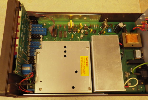
Another 4 screws later it looks like this:


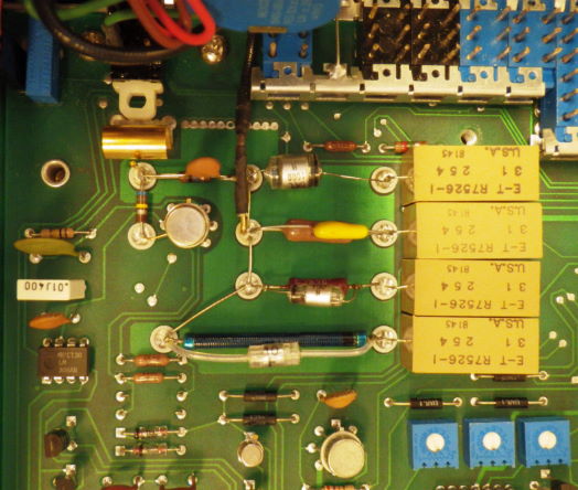
As already suspected/stated by free_electron, the (matched) FETs are in a single package with what I suspect is a custom number - probably it's specially selected devices: MP831-1010-8145 (last four digits might be the date code):


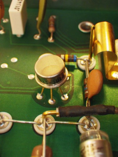
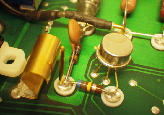
The reference FET is directly connected to the FR4 board, while the electrometer nodes are on ceramic insulators on top of the board. The gold-plated pin and sheet in the background is the zeroing of the input - mechanically mounted on the front-panel switch. The black heat-shrink tubing in the front is around the coax-lead from the input connector. Personally I do not like the carbon composite resistors (I assume that's what they are) in the input section, but these are mostly for overvoltage protection of the input anyway...

Another view of the input stage (this time with un-grounded input):


And finally the feedback resistors:

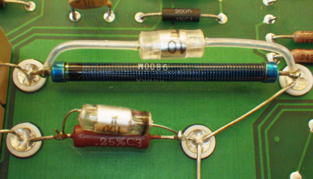
As you can see: no guarding of the resistors' bodies themselves apart from the ground plane underneath and the aluminum cage (removed) above...

« Last Edit: February 21, 2014, 08:11:36 pm by uwezi »
 

Offline don.r

  • Frequent Contributor
  • **
  • Posts: 740
  • Country: ca
Re: Electrometer input stage
« Reply #14 on: February 21, 2014, 06:50:33 pm »
Thanks uwezi,

I was thinking of doing a teardown of my 614 but now I won't bother since I think you have captured all the salient bits.
 

Offline Vgkid

  • Super Contributor
  • ***
  • Posts: 2710
  • Country: us
Re: Electrometer input stage
« Reply #15 on: February 21, 2014, 07:47:59 pm »
Thanks for the internal pics, it is amazing how barren they are.
If you own any North Hills Electronics gear, message me. L&N Fan
 

Offline dannyf

  • Super Contributor
  • ***
  • Posts: 8221
  • Country: 00
Re: Electrometer input stage
« Reply #16 on: February 21, 2014, 08:13:25 pm »
Quote
Ok, here it comes:

Wow!

That's engineering.
================================
https://dannyelectronics.wordpress.com/
 

Offline uwezi

  • Supporter
  • ****
  • Posts: 272
  • Country: se
    • GreenPhotons
Re: Electrometer input stage
« Reply #17 on: February 21, 2014, 08:30:27 pm »
Thanks for the internal pics, it is amazing how barren they are.

PCB real estate was not really an issue those days, and I guess when it comes to this sensitivity you need to keep things apart.

By the way: the lowest current range is 20 pA and the resolution 10 fA, settling time at this range 0.6 s.

Under the second metal cage there used to be a battery pack for floating operation.


Offline plesaTopic starter

  • Frequent Contributor
  • **
  • Posts: 965
  • Country: se
Re: Electrometer input stage
« Reply #18 on: February 22, 2014, 08:36:58 pm »
Thanks again UWEZI, the pictures are awesome. it so nice instrument. For me it is state of art...
Are the standofs really ceramic or PTFE?
I found the 2N5904 from Intersil and company called Solitron.
Thanks Dr. Conrad for the 610 schematic tip.
I will start first prototype with the LMP7721.
« Last Edit: February 22, 2014, 08:46:54 pm by plesa »
 

Offline uwezi

  • Supporter
  • ****
  • Posts: 272
  • Country: se
    • GreenPhotons
Re: Electrometer input stage
« Reply #19 on: February 22, 2014, 09:00:45 pm »
Are the standofs really ceramic or PTFE?

I must admit that I am not completely sure, but I can re-open the 6 screws next week. From the looks I still would believe it is ceramics rather than PTFE. The main issue here are leakage currents and those you can keep low with both materials.


Offline TiN

  • Super Contributor
  • ***
  • Posts: 4543
  • Country: ua
    • xDevs.com
Re: Electrometer input stage
« Reply #20 on: February 22, 2014, 09:43:15 pm »
K2001/2002 have dual JFET from Interfet (IFN146) in TO71 6-pin package. It's used in bootstrap circuitry.
I published schematics and datasheets around them before in my threads.
YouTube | Metrology IRC Chat room | Let's share T&M documentation? Upload! No upload limits for firmwares, photos, files.
 

Offline don.r

  • Frequent Contributor
  • **
  • Posts: 740
  • Country: ca
Re: Electrometer input stage
« Reply #21 on: February 22, 2014, 10:35:12 pm »
Are the standofs really ceramic or PTFE?

I must admit that I am not completely sure, but I can re-open the 6 screws next week. From the looks I still would believe it is ceramics rather than PTFE. The main issue here are leakage currents and those you can keep low with both materials.

It looks like teflon to me. Doesn't have that ceramic sound when I touch it with a metal screw driver.
« Last Edit: February 22, 2014, 10:45:26 pm by don.r »
 

Offline uwezi

  • Supporter
  • ****
  • Posts: 272
  • Country: se
    • GreenPhotons
Re: Electrometer input stage
« Reply #22 on: February 22, 2014, 11:13:58 pm »
Are the standofs really ceramic or PTFE?
It looks like teflon to me. Doesn't have that ceramic sound when I touch it with a metal screw driver.

That would have been my test as well. However, the pads appear to be hollowed out and filled with solder in order to support the components' wires, but PTFE would probably not give permanent support to this solder. Of course there are other good plastic insulators than just PTFE, but most of those would melt in contact with molten solder...
 

Offline don.r

  • Frequent Contributor
  • **
  • Posts: 740
  • Country: ca
Re: Electrometer input stage
« Reply #23 on: February 23, 2014, 01:49:32 am »
Are the standofs really ceramic or PTFE?
It looks like teflon to me. Doesn't have that ceramic sound when I touch it with a metal screw driver.

That would have been my test as well. However, the pads appear to be hollowed out and filled with solder in order to support the components' wires, but PTFE would probably not give permanent support to this solder. Of course there are other good plastic insulators than just PTFE, but most of those would melt in contact with molten solder...

My old HP 5335A has the same teflon rings on its input FET connections. The solder seems to hold.. ahem.. VERY well.  |O

BTW, don't forget to follow the guidelines in the Keithley 614 manual when replacing front end parts in an electrometer. The parts need to be extra clean before soldering them in. This applies to all electrometers.
 

Offline plesaTopic starter

  • Frequent Contributor
  • **
  • Posts: 965
  • Country: se
Re: Electrometer input stage
« Reply #24 on: February 23, 2014, 06:50:49 pm »
BTW, don't forget to follow the guidelines in the Keithley 614 manual when replacing front end parts in an electrometer. The parts need to be extra clean before soldering them in. This applies to all electrometers.

Yes, I have lot of experience with repairing their picoammeters like 6485/6487. It was enought to cleang it with IPA after soldering and bake at 50°C for few hours.
One time we sucessfully tried cleaning it with plasma used before high voltage potting componds. But it is strong enough to remove PCB soldermask, which is too much I suppose
Again, thanks all for support and pictures.


Share me

Digg  Facebook  SlashDot  Delicious  Technorati  Twitter  Google  Yahoo
Smf