Author Topic: Isolators - die pictures  (Read 3522 times)

0 Members and 1 Guest are viewing this topic.

Offline NoopyTopic starter

  • Super Contributor
  • ***
  • Posts: 1734
  • Country: de
    • Richis-Lab
Isolators - die pictures
« on: December 17, 2021, 03:41:06 pm »
I will post isolators in this topic.
The overview can be found here: https://www.richis-lab.de/iso.htm
I have moved the optocoupler H11L1 into this section: https://www.richis-lab.de/Opto01.htm

And now let´s take a look into the famous Burr-Brown ISO120!  8)


The ISO120 isolates signals up to 1500Vrms, 2121VDC, 20kV/µs. There is also the ISO121 which isolates up to 3500Vrms. The isolator uses a very special DIL-24 package were some pins are dropped.


There is a schematic in the datasheet explaining how the ISO120 works. The analog input is converted into a PWM modulated squarewave. This is done by the integrator A1 feeding a Schmitt Trigger that drives two 1pF capacitors that couple the signal to the receiver side. Two more 1pF capacitors are used in a feedback loop. In this feedback loop there is the sense amplifier switching a 200µA current source. With a constant 100µA current sink the sense amplifier switches 100µA or -100µA to the input of the integrator A1. You can add an additional external capacitor to A1 but you don´t need to. Bandwidth goes down with bigger integration capacitors but the other specifications are getting better. Additionally you can feed an external clock into the ISO120. (There is a small mistake in the schematic: The external clock is not shorted to Signal Com 1. ;)) There is some signal shaping before the clock is fed into the Schmitt Trigger. Depending on the clock frequency you have to add an external capacitor with the right value.
The receiver side is quite similar to the transmitter side. There are two S&H stages in the feedback path so you don´t see too much of the modulation frequency.
You can input +/-10V into the ISO120. The bandwidth is 60kHz. There are better specifications in the datasheet for a bandwidth of 6kHz: Offset is +/-5mV with a TC of +/-100µV/°C. Gain error is +/-0,04%FSR, +/-5ppm/°C. Nonlinearity is +/-0,005%FSR.


There are two dies in the two compartments of the ISO120. You can´t see the galvanic isolation that is inside the ceramic package.


There is quite some free area on the transmitter die.


CIC01525, a typical Burr-Brown number.


Burr-Brown used 12 masks.


We know these structures from other Burr-Brown circuits with tuned resistors. Some of the squares name A to U are cut by the laser. I don´t know what this tells us.


There is a test structure containing a transistor with two emitters.


We know these structures used to tune the laser tuning process.
It seems like the testpads that have to be contacted in production are equipped with small metal squares around the sides.

Offline NoopyTopic starter

  • Super Contributor
  • ***
  • Posts: 1734
  • Country: de
    • Richis-Lab
Re: Isolators - die pictures
« Reply #1 on: December 17, 2021, 03:42:28 pm »


Due to the big structures you can identify all parts of the circuit. At the upper edge there is the input resistor (yellow) and on the bottom edge there is the integration capacitor (yellow). The integrator A1 can be found in the middle of the die (blue). At the right edge there is the Schmitt-Trigger (cyan) containing the two 1pF feedback capacitors (green). The feedback is connected to the Sense amplifier (red) which switches the current source 200µA (pink) on top of the 100µA current sink (purple). In the upper right corner there is the signal conditioning for the external clock (orange) with a bias circuit (dark green). The ISO120 contains a voltage reference (white) with a bigger circuit supplying it and controlling the 100µA and the 200µA current source.


It looks like there is an option to change the input circuit. The bondpad Vin1 would give you half of the input resistance. Cin is connected to Com1 only but there is a metal line between this capacitor and the input resistor. Connected this would give you a low pass filter. It seems like Vin2 gives you the possibility to feed a current input directly into the integrator A1. Rt looks like a testpad.  :-//


Clock signal conditioning...


Here we see the bias circuit connected to the Schmitt Trigger.
The circuit is not connected to the reference circuit it just uses the normal supply.
The circuit is connected to an unused bondpad in the upper left corner of the die. It seems like it would be possible to modify the bias.


Here we see the integrator A1. In the upper left corner there is the input circuit with four criss-cross connected transistors to fight thermal drift. In addition there are two big tunable resistors to adjust the offset voltage. On the right side there is the output stage.


Here we see the Schmitt Trigger. The outputs of the circuit change sides before they are connected to the bondpads connecting the circuit to the isolation capacitors. In the middle of this cross connection there are pull-up resistors (yellow). The output transistors (red) and the feedback capacitors (green) are integrated in the same active area. The feedback lines are kept closely left and right to a GND1 line.


It seems like you can tune the size of the feedback capacitor with the help of an additional smaller area.


The sense amplifier gets its input from the right that is connected to capacitors in the first place (green). I assume these capacitors make the circuit more robust against common mode spikes. On the receiver side this sense amplifier is the only circuit directly connected to the coupling capacitors. There is a tuned feedback with a small capacitor (red) and a big resistor. The output is supplied differentially by two transistors (cyan) that are supplied by a current source (yellow).


The switchable current source is interesting. At the lower edge there is the 100µA current sink constructed with two current mirrors (cyan). The current mirrors are controlled by the reference circuit. They are based on one single current sink (blue) that is not connected to the reference circuit. Perhaps the common current sink was necessary for proper startup.
The 200µA current source consists of two transistors CL and CH. The current is controlled by the reference circuit. The sense amplifier switches between these two transistors. The circuit switches 200µA to the input or the output of the integrator A1. That´s beneficial because in this configuration the integrator A1 always has to sink 100µA (0V at the input). It sinks 100µA of the 200µA, 100µA charging the capacitor or it sinks 100µA which charges the capacitor the other way.


The ISO120 has a bandgap reference on board. You can clearly see the four transistors with two emitters each that are connected in parallel and integrated around a second transistor. More information about bandgap references can be found in the article about the TL7705 (https://www.richis-lab.de/TL7705.htm) or in the article about the AD1403 (https://www.richis-lab.de/REF16.htm). One deviation is that there is only one emitter resistor connected to the bigger transistor (yellow). There is no common resistor that amplifies the positive TC to get near zero TC. I assume the additional positive TC is generated in the "supply circuit".
The reference voltage isn´t used directly but it generates a reference current apparently with the big tuned resistor connected to the bases of the bandgap transistors (cyan). Two transistors (green) placed in the supply of the reference (red) are connected to the reference voltage node (white).


The supply circuit is tuned at the lower edge with a tunable resistor in a current mirror and a testpad.
In this area the control signals for the 100µA and the 200µA current sources are generated.
 
The following users thanked this post: capt bullshot

Offline NoopyTopic starter

  • Super Contributor
  • ***
  • Posts: 1734
  • Country: de
    • Richis-Lab
Re: Isolators - die pictures
« Reply #2 on: December 17, 2021, 03:43:38 pm »


The receiver ist quite similar to the transmitter. Instead of the Schmitt Trigger there is an output amplifier and at the lower edge we can see two large Sample&Hold stages.


The name of the receiver is the same as the name of the transmitter and there are no mask revisions. Perhaps transmitter and receiver are manufactured with one mask set because you need the same number of transmitter and receiver dies and production tolerances compensate each other. That would explain why there is a lot of free space on the transmitter die.


The lines connecting the isolation capacitors to the sense amplifier are impedance matched.


The S&H stages are based on a lot of current sources. The bigger capacitors are probably for saving the sampled voltage.


That is the output stage with a highside (red) and a lowside (cyan) transistor.


At the output bondpad there is a overcurrent protection based on a series resistance (blue). The width of the resistance area can be varied adjusting the current limit. A high output current activates a transistor (green) reducing the current of a current source of the S&H stage. That probably reduces the output level.
A diode (yellow) limits the input current. It is connected to the output amplifier circuit. The current limit circuit probably works similar to the current limit circuit in the LF355 (https://www.richis-lab.de/Opamp15.htm).
There is a feedback line (cyan) connecting the output bonpad to the S&H stage.


On the transmitter die there are two T in the right corners. On the receiver die there are two R in the left corners.  :-+


https://www.richis-lab.de/iso01.htm

 :-/O

Offline T3sl4co1l

  • Super Contributor
  • ***
  • Posts: 21688
  • Country: us
  • Expert, Analog Electronics, PCB Layout, EMC
    • Seven Transistor Labs
Re: Isolators - die pictures
« Reply #3 on: December 17, 2021, 08:04:24 pm »
Neat!

Have seen that one many times (in books, catalogs..), can't say I was ever desperate enough to buy one though. :-DD

Tim
Seven Transistor Labs, LLC
Electronic design, from concept to prototype.
Bringing a project to life?  Send me a message!
 

Online RoGeorge

  • Super Contributor
  • ***
  • Posts: 6203
  • Country: ro
Re: Isolators - die pictures
« Reply #4 on: December 17, 2021, 09:07:55 pm »
Oh, so more gold, thank you!  :-+
Subscribed.

Offline NoopyTopic starter

  • Super Contributor
  • ***
  • Posts: 1734
  • Country: de
    • Richis-Lab
Re: Isolators - die pictures
« Reply #5 on: July 24, 2022, 04:29:28 am »


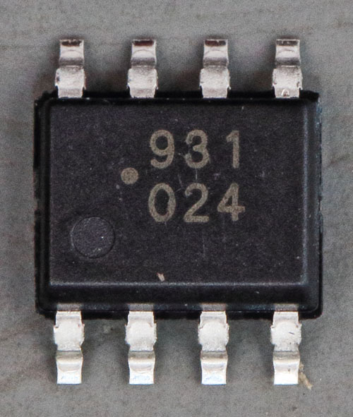
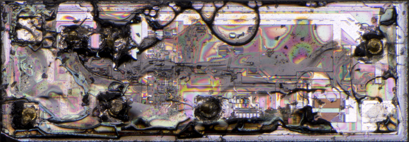
Broadcom HCPL-0931, this one took me quite some time...

The HCPL-0931 is a fast digital isolator. The datasheet specifies an isolation voltage of 2,5kVrms. However the maximum continuous operating voltage is just 150Vrms (300Vrms for the HCPL90xx). 3,3V and 5V TTL/CMOS signals can be transmitted at up to 100MBd. It is robust against common mode pulses with rise times up to 15kV/µs.


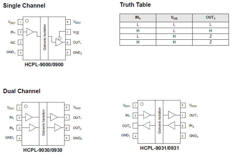
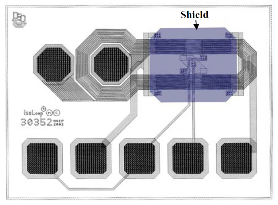
The HCPL-0931 contains two channels with opposite transmission directions. In parallel Broadcom offers other variants and also multi-channel isolators.


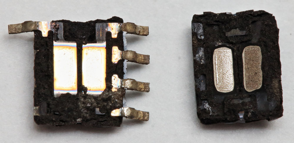
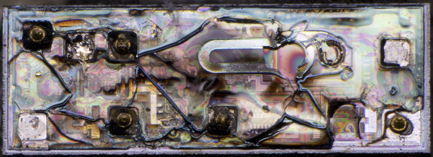
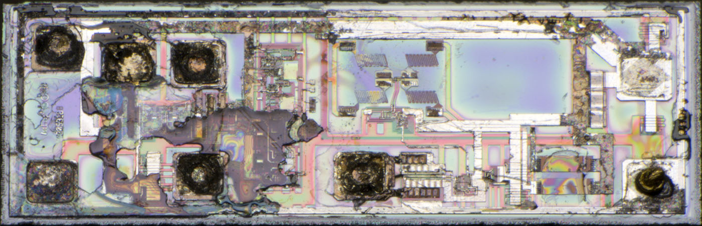
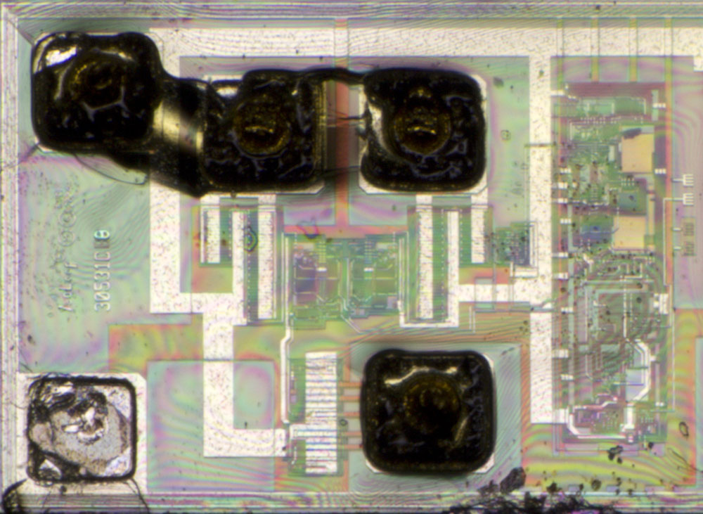
In the package you can find two long dies, which are placed next to each other with some distance between them.


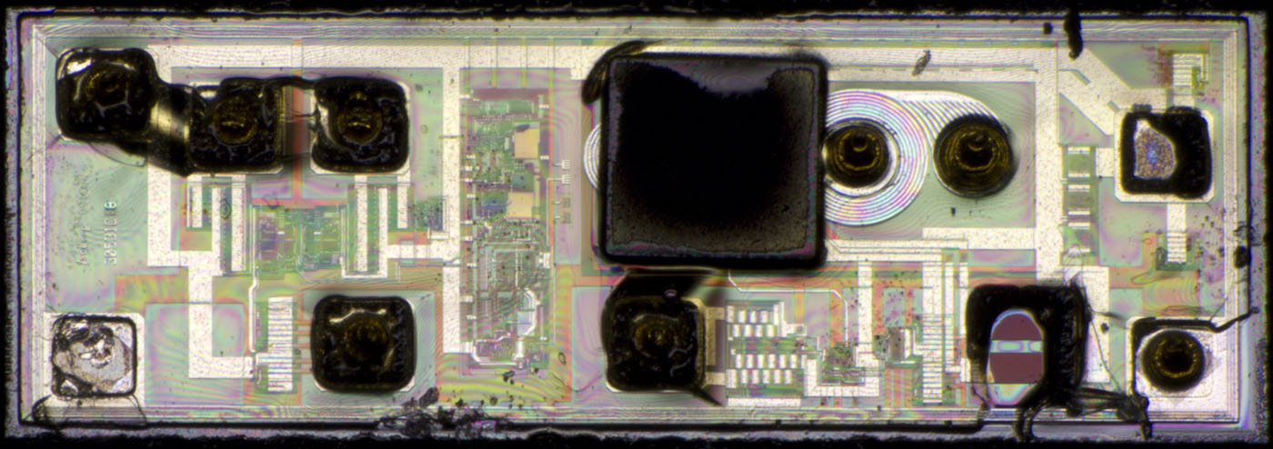
The dimensions of one die are 1,9mm x 0,7mm.


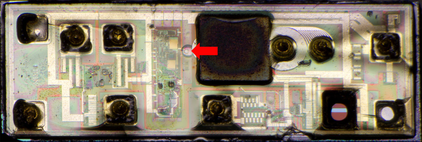
The two dies differ just in a slightly different arrangement of bonding wires and a small round cutout in the top insulation layer that appears to expose a test pad.


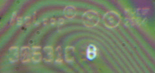
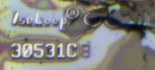
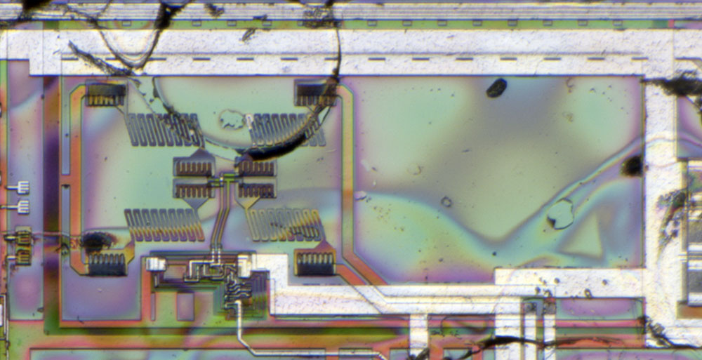
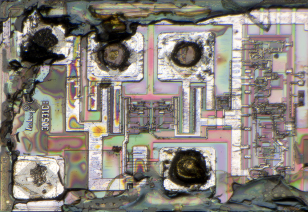
On one edge of the die is the word IsoLoop, the name for an insulation technique used by the company NVE. Next to the copyright signs the logo of the company NVE seems to be depicted, in which the horizontal lines of the E are extended to the right. NVE is an independent company but appears to have partnered with Broadcom. NVE has a very similar isolator in the IL612 from the IL600 series. Perhaps this is even the same die.

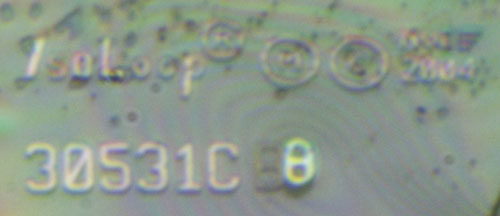
The design is apparently from 2004 and the internal designation is 30531CBB. The last two characters are shown with different materials than the first characters. It is quite possible that they document revisions to the masks used to build these layers.


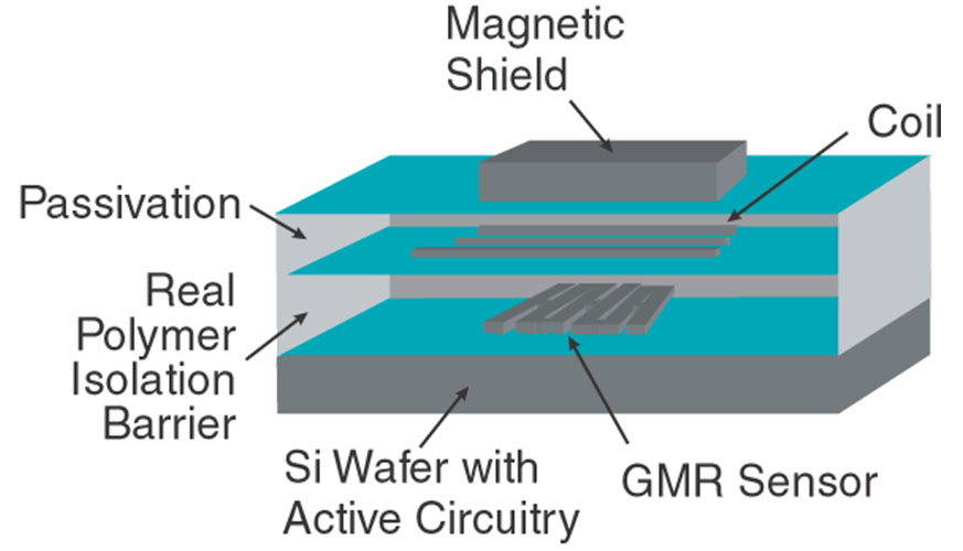
In the presentation "NVE IsoLoop® Isolator Overview" NVE shows the basic design of their isolators. On a wafer there is a magnetic field sensor based on the GMR technology. The polymer layer that follows represents the device's insulating path. On top of the isolation there is the coil that generates the exciting magnetic field. The coil is protected by a passivation layer. A magnetic shield is applied on top of the passivation layer. This not only shields external magnetic fields, it also concentrates the magnetic field of the coil too.


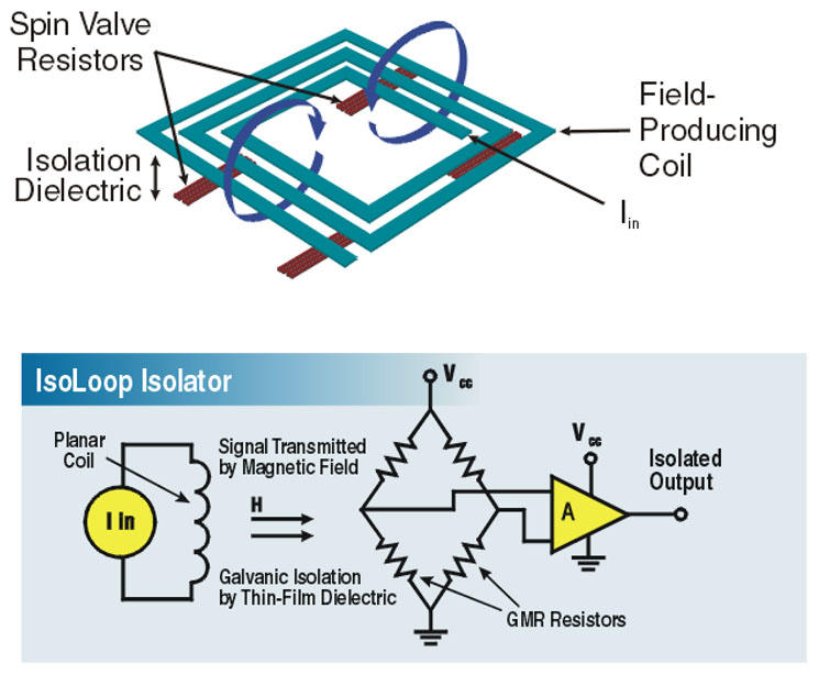
The NVE presentation shows that the magnetic field is evaluated via a Wheatstone bridge. The use of a Wheatstone bridge guarantees a high robustness against external magnetic fields.


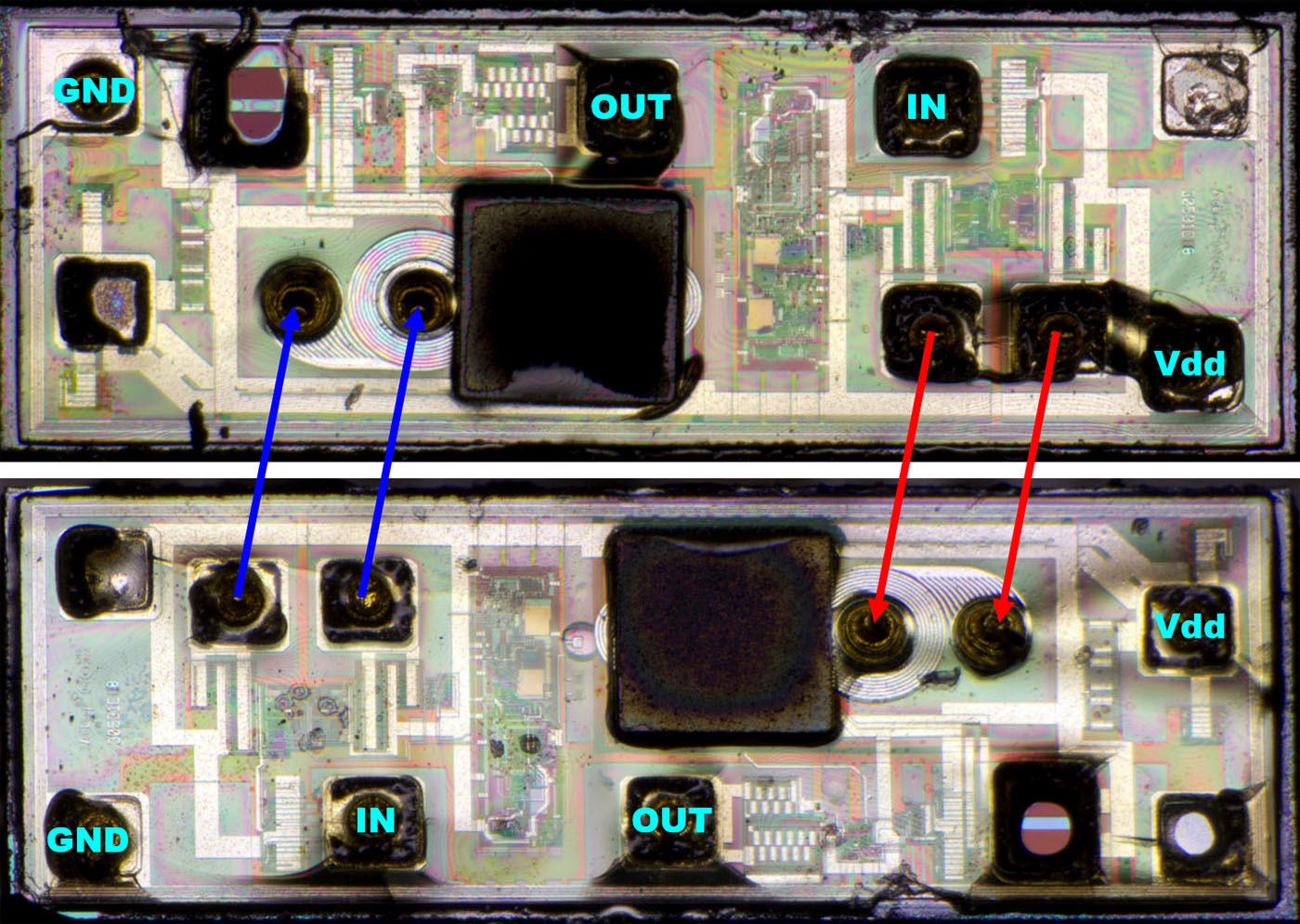
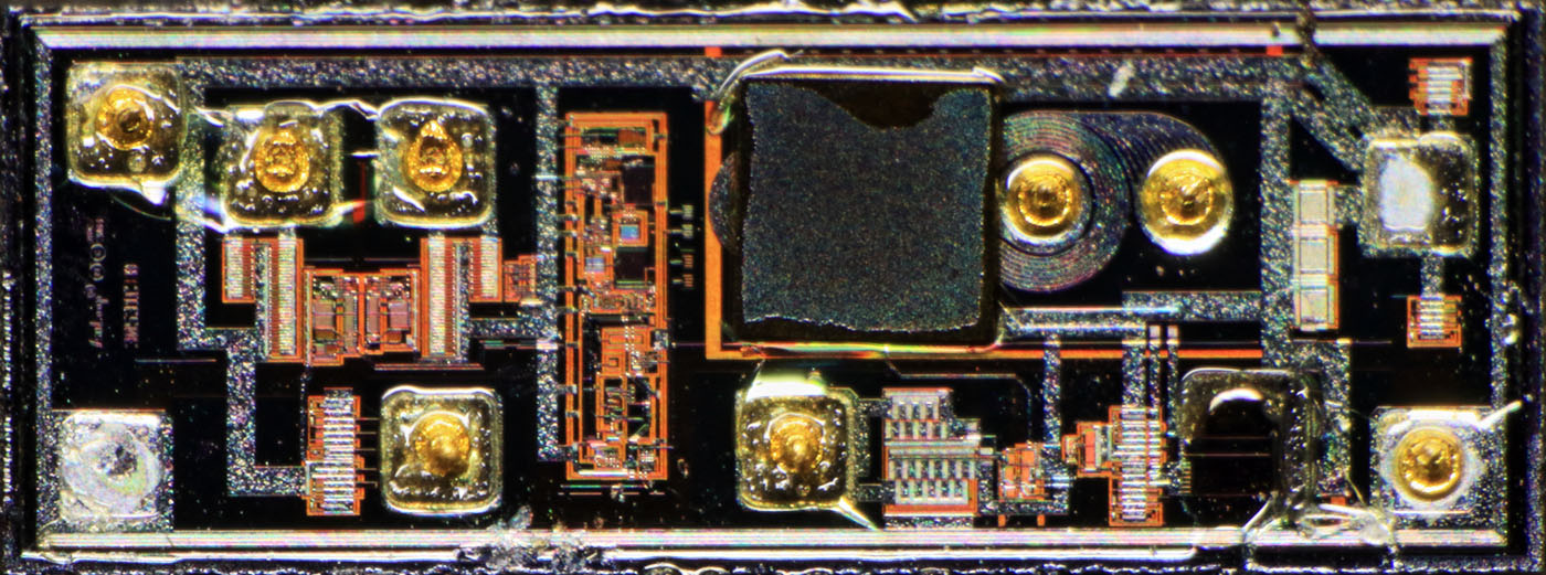
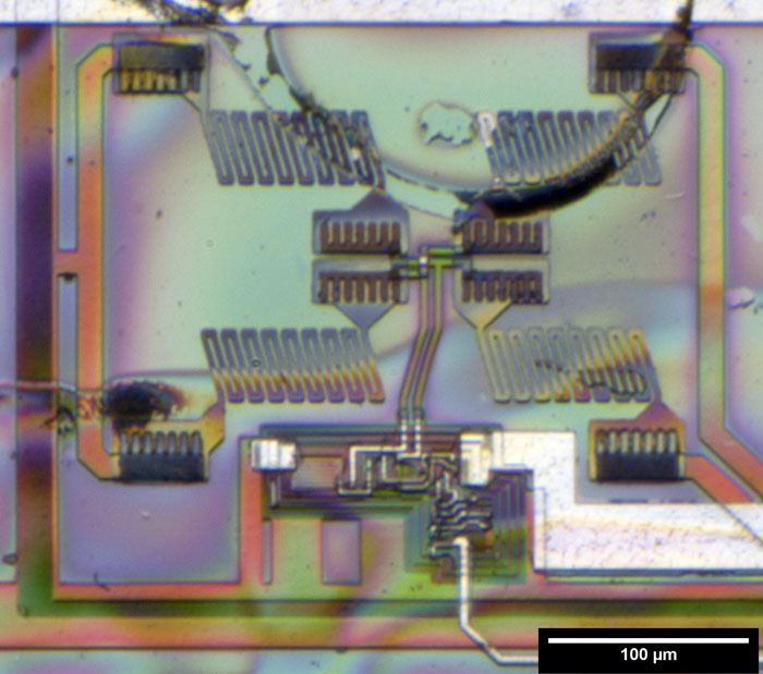
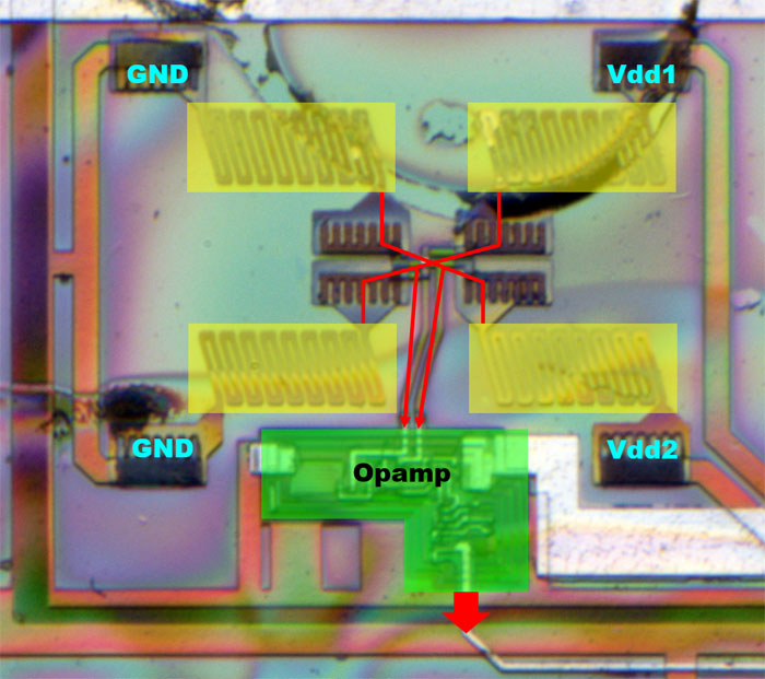
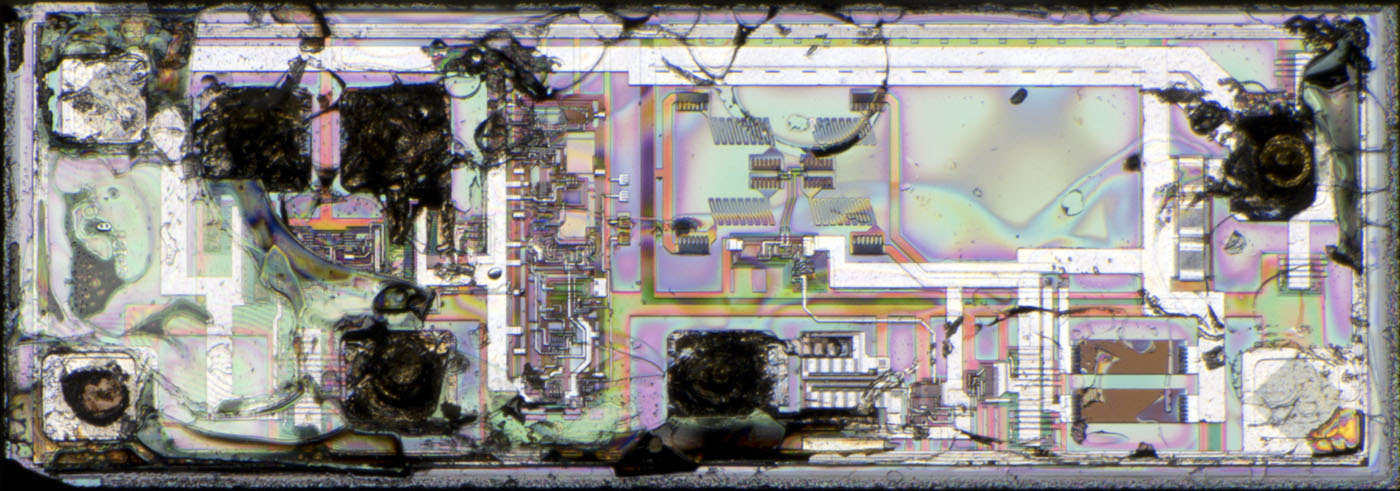
With the information so far it is already possible to reconstruct how the dies were arranged in the housing and how the bondwires were used.


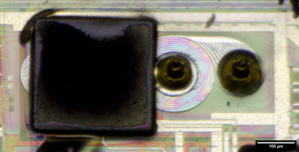
The core element, the magnetic circle, has a square, black shield. Parts of the coil arrangement can be seen on the sides of the shield.


NVE staff have written an IEEE article called "Linear Spin-Valve Bridge Sensing Devices." There the structure of a GMR-Wheatstone bridge is shown, which fits quite well to the HCPL-0931. The designation and logo are very similar too.


The polymer layer on the die can be gradually decomposed by applying a well-dosed, increased temperature.


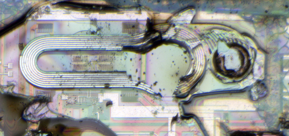
Here the magnetic shielding is already missing, the coil can still be seen.


The polymer layer can be decomposed almost completely, but care must be taken not to degenerate the remaining structures as well.


Under the remains of the coil, the Wheatstone bridge is revealed.


The supply voltage is fed to the Wheatstone bridge from the right. The reference potential is located on the left. The four GMR elements (yellow) are routed in serpentines. The contacts between the GMR elements and the continuing lines are conspicuously large.

The evaluation of the differential voltage of the Wheatstone bridge takes place directly below the GMR elements, so that as little interference as possible couples in on the line up to there. The processed signal is output downwards.


The polymer layer cannot be completely removed without also endangering the remaining structures.


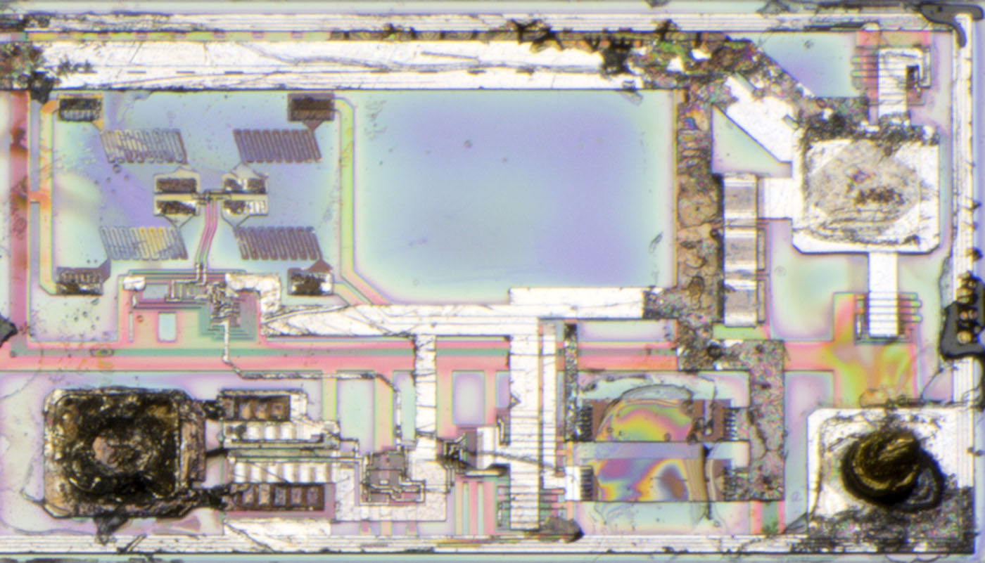
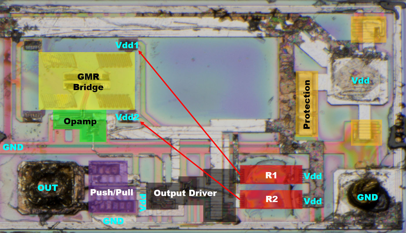
The receiver occupies the right area of the die. The structures around the Vdd bondpad appear to be protective structures.

Two Vdd potentials are fed to the Wheatstone bridge via two resistors. Above these two resistors, the polymer layer was cut out and the traces of an alignment can be seen.

The operational amplifier of the Wheatstone bridge is followed by a driver and a push-pull output stage, which serves the output of the HCPL-0931.


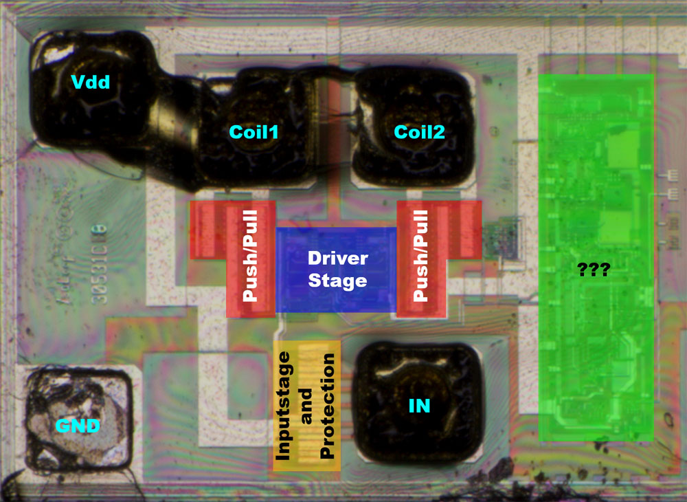
On the left side of the die is the receiver section. Below the bondpads, which are connected to the coil on the other die, you can see push-pull transistors. Consequently, the driving is done with an H-bridge. The drivers are integrated between the push-pull transistors. The structures at the input bond pad certainly represent some protection function.

The function of the circuit on the right side remains unclear. It is only connected to the driver of the transmitter coil. According to the NVE presentation, the signal to be transmitted is not modulated. Therefore an oscillator can be excluded. Maybe it is a current control, which ensures that the receiver side is sufficiently modulated, but not overdriven.  :-// The uncovered test pad described above could have been used for an adjustment of such a control.


https://www.richis-lab.de/iso02.htm

 :-/O
 
The following users thanked this post: doktor pyta, RoGeorge, Miyuki, ch_scr, MegaVolt

Offline NoopyTopic starter

  • Super Contributor
  • ***
  • Posts: 1734
  • Country: de
    • Richis-Lab
Re: Isolators - die pictures
« Reply #6 on: September 17, 2022, 08:07:42 am »


This H11L3, produced in 1996, was manufactured by QT Optoelectronics. QT Optoelectronics is now part of Fairchild.

The H11L3 is functionally equivalent to the H11L1 from General Electric (https://www.richis-lab.de/Opto01.htm), so it contains an optocoupler with a Schmitt trigger at the output and transmits a digital signal with a frequency of up to 1MHz. The last number stands for the bin. While the LED of the H11L1 typically needs only 1mA to switch the output, the H11L1 must be supplied with 3mA.


Unlike General Electric's H11L1 the electronics in QT Optoelectronics' H11L3 is embedded in a relatively large, silicone-filled cavity.


With an edge length of 0,3 mm the installed LED is just as big as the LED of General Electric's H11L1. However the metal contact is much smaller. This increases the free area that can emit light, but probably worsens the current distribution at the same time.


The receiver is integrated on a die with an edge length of 1,26mm. The metal layer that protects the receiver circuit from light incidence is particularly striking. Light can generate free charge carriers in the circuit, which would lead to unwanted current flows. The effort is remarkable, since the relatively simple circuit has to be manufactured with a process that offers a second metal layer.


The light-sensitive area is divided into two areas. In the H11L1 from General Electric the ground potential is the reference potential of the light-sensitive area, here it is the supply potential.

The sensor area is connected to a testpad, which probably should allow to determine the light sensitivity of the area. In the right area some small resistors can be seen, which most likely can be used to adjust the sensitivity of the evaluation circuit.


In the lower right corner of the die is the output. At first glance the surrounding structures remind us of a push-pull output stage. The element between the bond pads is clearly recognizable as a lowside transistor. However, the element to the left of the output just connects the output with the base of the lowside transistor. It could be that it is a Z-diode that drives the lowside transistor as overvoltage protection in case of a too high voltage at the output.


https://www.richis-lab.de/Iso03.htm

 :-/O
 
The following users thanked this post: RoGeorge, ch_scr

Offline NoopyTopic starter

  • Super Contributor
  • ***
  • Posts: 1734
  • Country: de
    • Richis-Lab
Re: Isolators - die pictures
« Reply #7 on: July 10, 2023, 02:02:37 pm »


The Burr-Brown ISO121 is an isolator for analog signals. It offers the same features as the extensively documented ISO120, but the galvanic isolation is guaranteed up to 3500Vrms (4950V DC). To be able to represent this isolation strength, one has chosen a significantly larger package than the ISO120 (DIP40 compared to DIP24).


The design of the ISO121 is the same as for the ISO120. The transmitter and receiver are located on the outer edges of the housing. Connection pins are also only placed in this area in order not to unnecessarily reduce the insulation strength. The capacitive coupling between transmitter and receiver takes place inside the ceramic body.


It turns out that the ISO121 uses exactly the same integrated circuits as the ISO120.


https://www.richis-lab.de/iso04.htm

 :-/O
 
The following users thanked this post: RoGeorge, ch_scr, iMo

Offline NoopyTopic starter

  • Super Contributor
  • ***
  • Posts: 1734
  • Country: de
    • Richis-Lab
Re: Isolators - die pictures
« Reply #8 on: December 17, 2023, 08:20:04 pm »


The AD6C111 is a solid state relay from the American company Solid State Optronics. The insulation capability between control and load is at least 5000V. There is a light emitting diode on the input side. The load side has a certain hysteresis, so that the relay typically switches on at a current of 1,75mA through the LED and switches off again at 0,5mA at the latest. The switches at the output isolate up to a voltage of 400V. Up to 120mA may flow in the conductive state. The resistance is typically 17Ω. The module usually requires 0,75ms to switch on. When switching off, 0,05ms can be expected.


The circuit diagram in the datasheet shows that there are two antiserial MOSFETs on the output side. Pin 5 is a center tap. According to the datasheet, these are DMOS transistors.


If you open the package, a white mass becomes visible. Underneath is the LED and the control circuit for the power transistors. The power transistors are located in the upper corners of the housing. The individual elements are each placed on their own lead frame elements.


When the semiconductors are exposed, both the led and the control circuit become detached.


The edge length of the led is only 0,32 mm. The surface is surprisingly rough.


The component shown here has been opened up so that the underside of the internal structure can be seen. The two power transistors are clearly visible in this picture. In the lower area you can see the carrier of the led, which leads from pin 1 to the center.


The dimensions of the power transistors are 1,0mm x 1,1mm. The characters VF05 are an indication of the transistor type.


The data books of the American semiconductor manufacturer Supertex contain images of a MOSFET design that exactly matches the die in question. This design was used for several DMOS transistors and bears the designation VF05.


After removing the control circuit, you can clearly see that the white material is just a protective layer surrounding a clear potting compound.


The clear potting material serves as a light guide between the led and the control circuit.


The control circuit is 1,6mm x 1,3mm in size.


Fourteen photodiodes connected in series take up a large part of the surface. The photodiodes fulfill a dual function. They receive the light from the LED, thus serving as a receiver for the control signal and at the same time generating the energy required to operate the circuit. The active areas of the photodiodes have an edge length of 0,25 mm.


The insulating frames look like the isolation in the TP1322 (https://www.richis-lab.de/Opamp49.htm). They are very thin, have rounded corners and their surfaces are textured. This would suggest that the AD6C111 has dielectric insulation.

Two unused structures show the typical structure of NPN transistors. Within the contacted green area, which obviously represents the base area, there is a smaller contacted area, which represents the emitter. The third contact is then the collector connection, under which a strong n-doping ensures a low-resistance connection.


The die has two metal layers. The upper metal layer is mainly used to shade the circuit so that the light from the LED does not generate uncontrolled current flows.


If you remove the metal layer, the function of the circuit becomes clearer.


The large structure in the lower area stands out visually. This is a resistor. Various elements can be seen under the resistor structure. One of these structures must represent a connection to the substrate so that the control of the MOSFETs has a reference potential. Whether the other elements have a relevant function or are just test structures remains unclear.

On the left you can just make out two lines. These could be artifacts without a function. The third structure from the left appears to have been contacted by the metal layer. The third structure from the right could be the contact from the resistor to the substrate. The two elements on the right could be alternative contacts.


The circuit is not too complex. The typical structure of a PNP transistor and a resistor are located under the upper metal layer. The base-collector areas of NPN transistors are used for the two capacitances C1 and C2.


The circuit is constructed in such a way that it represents a certain hysteresis. If the photodiodes supply a small current, this flows via the emitter-base path of the transistor Q1 and the resistor ladder R1/R2/R3. According to its current amplification, Q1 directly short-circuits a large part of the current and the power transistors remain inactive.

If the current from the photodiodes increases, the voltage that drops across the resistors increases. As a result, the drive of transistor Q1 is reduced and the current continues to increase via the resistor ladder. This is a self-amplifying process. The current from the photodiodes initially flows directly back via the collector of Q1 and, from a certain value, is largely fed into the resistor ladder. Two voltages then drop across the resistors R1 and R2, which serve as the gate-source voltage for the two power transistors and activate them.

If the current from the photodiodes is reduced, the transistor Q1 becomes conductive again at some point and the current flow switches relatively quickly from the resistor ladder to the collector path of the transistor. Capacitors C1 and C2 ensure that the circuit does not oscillate.


https://www.richis-lab.de/iso05.htm

 :-/O
 
The following users thanked this post: RoGeorge, ch_scr

Offline NoopyTopic starter

  • Super Contributor
  • ***
  • Posts: 1734
  • Country: de
    • Richis-Lab
Re: Isolators - die pictures
« Reply #9 on: December 18, 2023, 08:51:20 am »
Aaaaah, what did I do!?  |O

That should be more correct:


Of course you need positive Vgs to switch the MOSFETs on.

It was a long day yesterday...  ;D
 
The following users thanked this post: ch_scr

Offline PDP-1

  • Contributor
  • Posts: 15
  • Country: us
  • Spacewar!
Re: Isolators - die pictures
« Reply #10 on: December 19, 2023, 04:26:12 am »
Have you ever looked into the Analog Devices ADuM series? They have both analog and digital isolators, I've only used the ADuM3190 analog chips back when the great parts shortage led to us not being able to get the AD210 modules that we had previously used.

When I was working on that design someone on another forum sent me some chip shots of the internals. Three chips - presumably input modulator, isolation transformers, and an output demodulator. 2500V isolation, but if you need more the ADum4190 can do 5000V. A downside of the ADuM3190 analog chip is that it is unipolar only, to get bipolar transmission I had to use the voltage references on the input/output side to add a bias on the input side and subtract it off the output side. Also, the linear input range is pretty limited. Luckily we did not need extreme accuracy/precision for this application so getting the transfer function to within 1% was good enough. 200kHz or 400kHz bandwidth depending on the chip variant.

The digital isolators come in a variety of IO channel counts but supposedly are good enough to handle USB 2.0 signals.
 

Offline NoopyTopic starter

  • Super Contributor
  • ***
  • Posts: 1734
  • Country: de
    • Richis-Lab
Re: Isolators - die pictures
« Reply #11 on: December 19, 2023, 10:37:08 am »
I have an ADUM somewhere here in stock. For sure sooner or later I will take some pictures. As you said and showed that should be very interesting!  :-+

Offline NoopyTopic starter

  • Super Contributor
  • ***
  • Posts: 1734
  • Country: de
    • Richis-Lab
Re: Isolators - die pictures
« Reply #12 on: December 20, 2023, 05:09:42 am »


I´m still not 100% sure about the behaviour of the circuit.

Right now I assume Q1 shorts most of the current as long as the photodiodes supply just a little current.
At some point the current is high enough that the current gain of this tiny lateral PNP transistor drops heavily. Due to this the current through Q1 drops and the voltage rises.
That should give us kind of a hysteresis effect.


Share me

Digg  Facebook  SlashDot  Delicious  Technorati  Twitter  Google  Yahoo
Smf