Author Topic: MEMS - nice die pictures  (Read 16141 times)

0 Members and 2 Guests are viewing this topic.

Online RoGeorge

  • Super Contributor
  • ***
  • Posts: 8502
  • Country: ro
Re: MEMS - nice die pictures
« Reply #25 on: October 02, 2022, 02:34:07 pm »
Great die shots even without electron microscope  :-+, thank for all the pics!
 
The following users thanked this post: Noopy

Offline NoopyTopic starter

  • Super Contributor
  • ***
  • Posts: 2410
  • Country: de
    • Richis-Lab
Re: MEMS - nice die pictures
« Reply #26 on: October 02, 2022, 02:41:55 pm »
Great die shots even without electron microscope  :-+, thank for all the pics!

Thank you for your ongoing support. Much appreciated.  :-+
 
The following users thanked this post: SeanB

Offline Yunphy

  • Newbie
  • Posts: 1
  • Country: us
Re: MEMS - nice die pictures
« Reply #27 on: September 22, 2023, 03:07:47 pm »
hi, have you got any photos of vesper? Do you want to share them with me?  ^-^
 

Offline NoopyTopic starter

  • Super Contributor
  • ***
  • Posts: 2410
  • Country: de
    • Richis-Lab
Re: MEMS - nice die pictures
« Reply #28 on: September 22, 2023, 05:26:18 pm »
No, sorry, no vesper MEMS up to now.

Offline NoopyTopic starter

  • Super Contributor
  • ***
  • Posts: 2410
  • Country: de
    • Richis-Lab
Re: MEMS - nice die pictures
« Reply #29 on: October 18, 2023, 03:43:52 am »


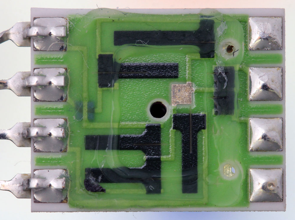
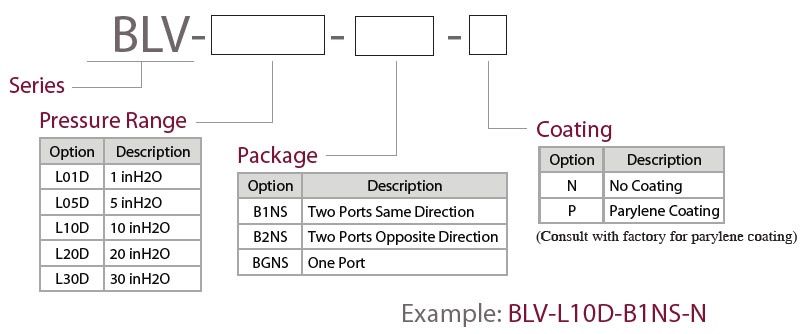
The company All Sensors offers piezoresistive pressure sensors. One product line bears the designation BLV, which is supplemented with further characters depending on the variant. The first block specifies the measuring range. The second block specifies whether the housing has one or two hose connections and in which direction they point. The sensor can also be coated with Parylene, which makes it more robust.
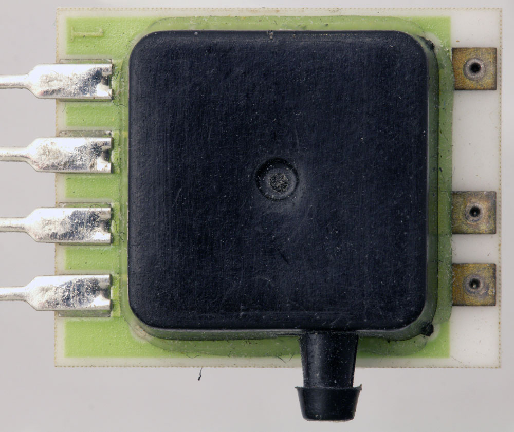
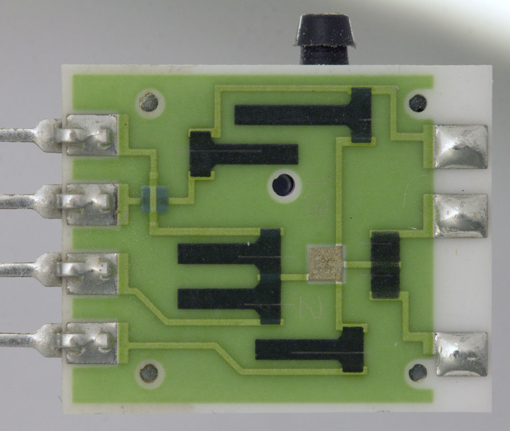


The module presented here has a hose connection on one side. It is based on a ceramic carrier with some tuned resistors on the non-closed side. A testpoint is used for tuning. Four pins are attached to one edge. There are vias on the other edge.
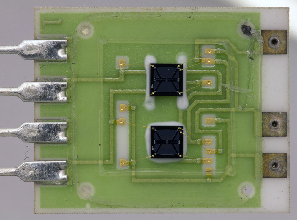


Two MEMS modules are located under the plastic housing.
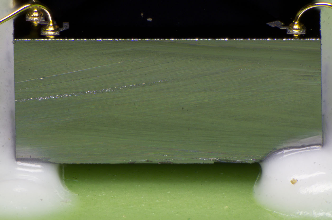


A closer look shows that one MEMS module is glued in such a way that the underside comes into contact with the surrounding atmosphere in the plastic housing. The second module has been glued around its entire circumference. Underneath, there is a hole in the ceramic carrier, which means that the underside of this module comes into contact with the atmosphere surrounding the sensor.

A closer look reveals that the modules are composed of two elements.
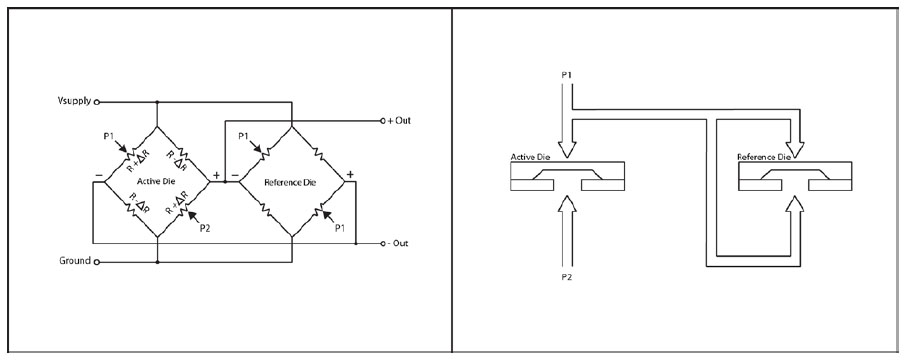


The manufacturer shows on his website how such a pressure sensor works. The configuration of the resistors as a Wheatstone bridge already compensates for many parasitic effects and thus enables an accurate determination of the pressure. Here, the behaviour of the pressure sensor was further improved with a second MEMS module. The second module does not experience any pressure difference and is just used to compensate for parasitic effects.
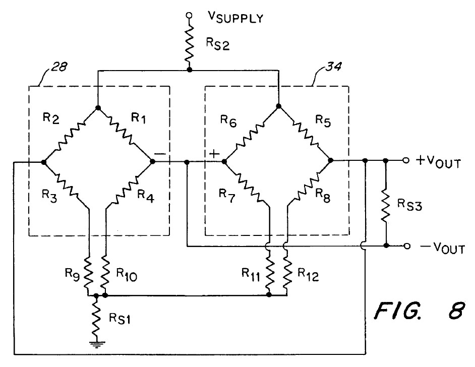


All Sensors refers to patent US6023978A, which belonged to Honeywell. There it shows that the circuitry is somewhat more complex and includes additional resistors.
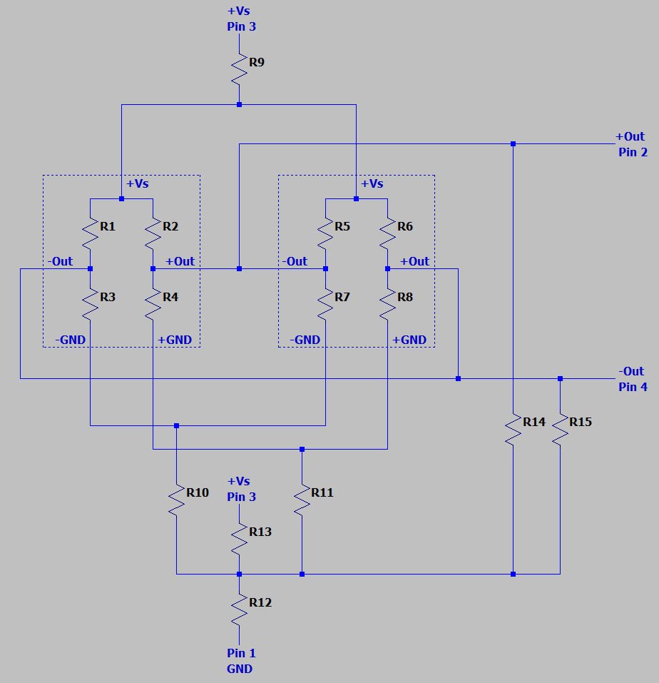


If we analyse the resistors and the wiring on the pressure sensor, it becomes apparent that the wiring here is somewhat more complex than shown in the datasheet. The symmetry of the two modules and the characteristic curve of the pressure sensor are extensively adjusted.
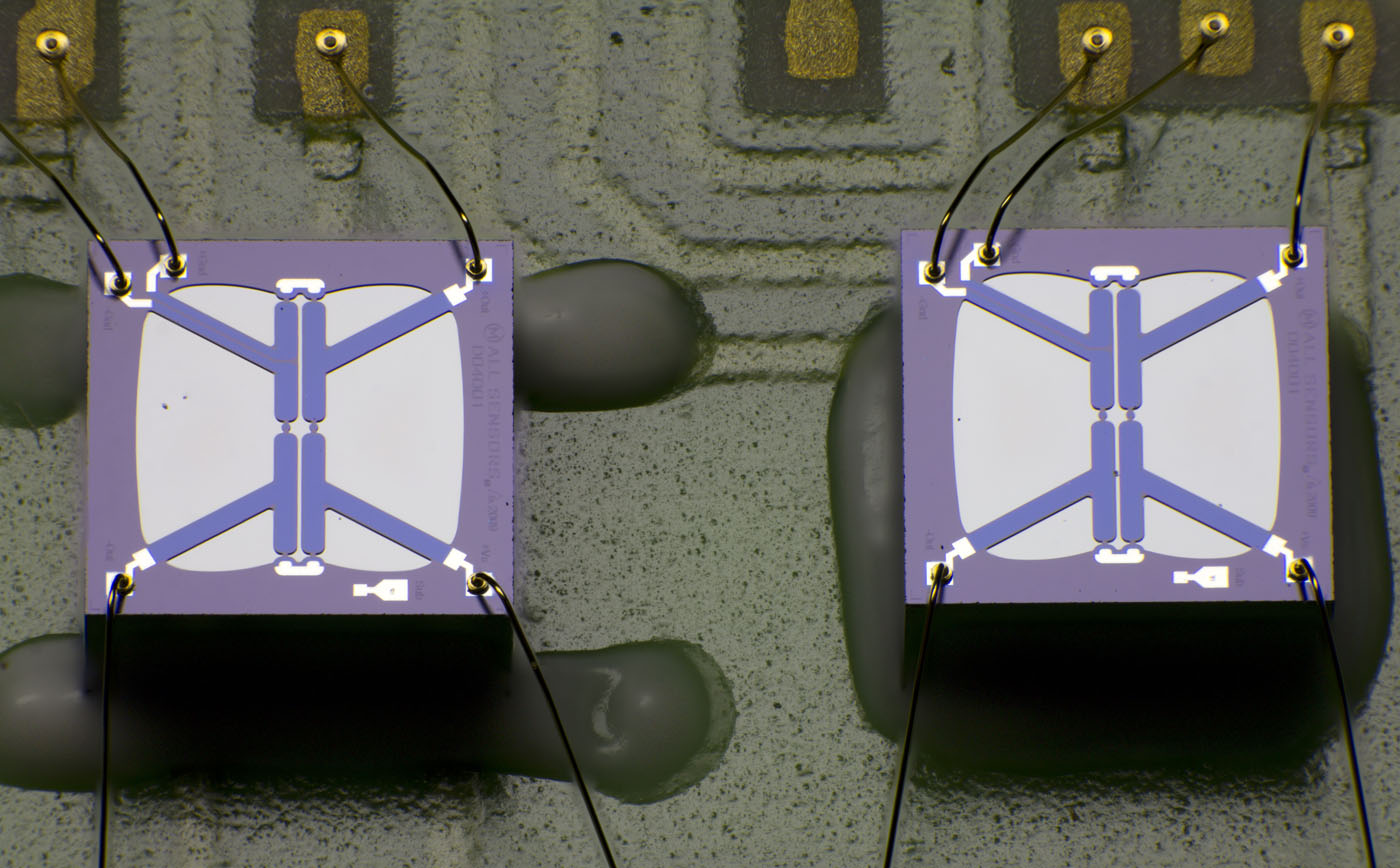


As was to be expected, the two MEMS modules are exactly the same.
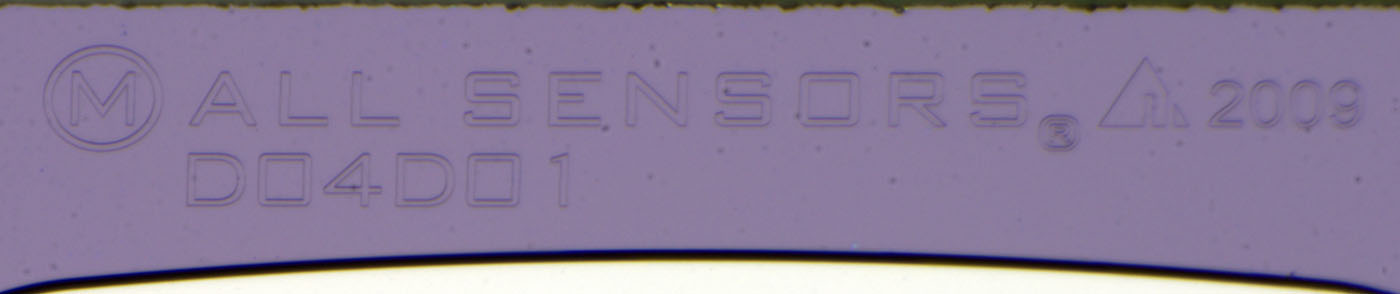


The design comes from All Sensors in 2009. DO4DO1 could be an internal designation of the design.
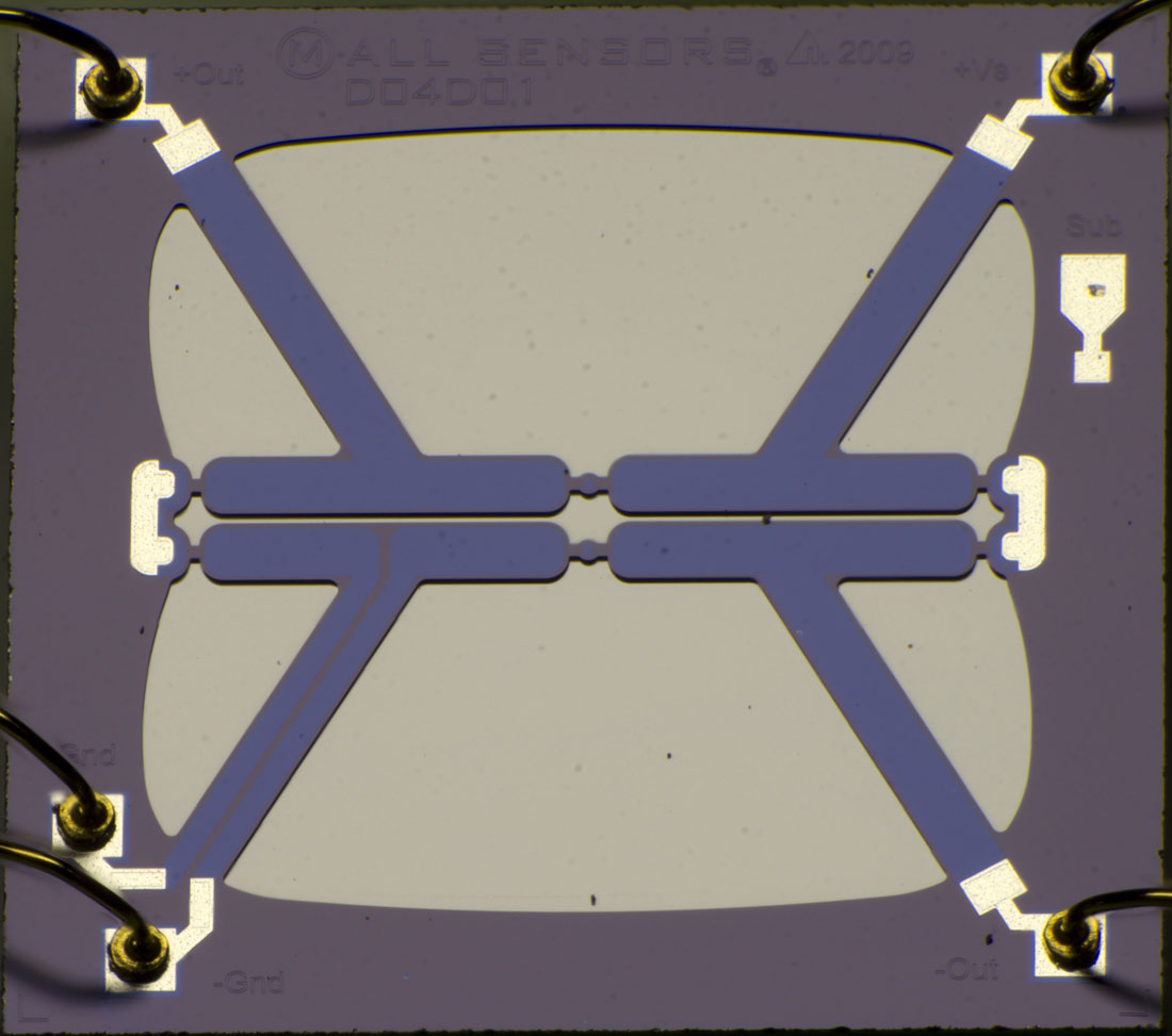


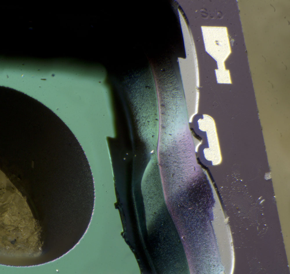
The structures show the symmetry that one would expect from such a module. However, the GND connection is doubled.
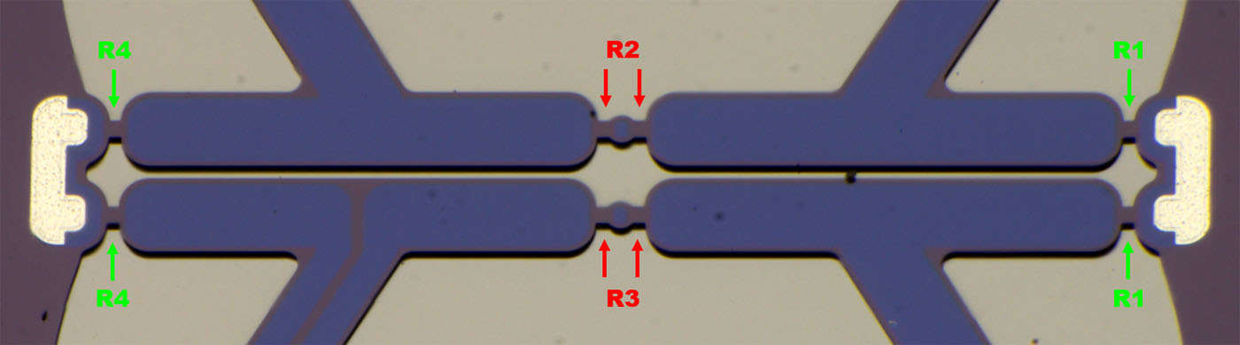
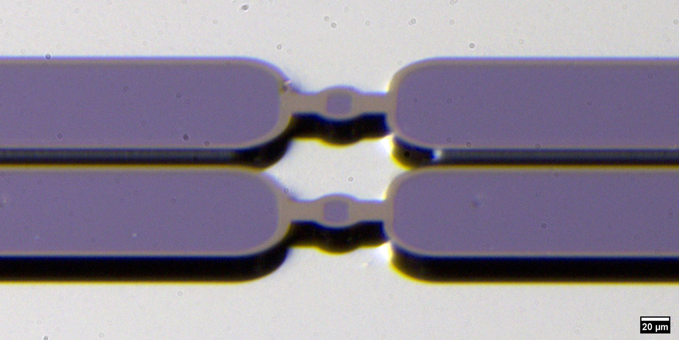


Pressure measurement is based on piezoresistive resistors that change their value when stretched or compressed. The active elements are not immediately visible. The resistors R2 and R3, which realise the pressure measurement, are located in the middle of the surface, which moves up or down depending on the pressure. It seems that the brownish base represents the piezoresistive material, which is accordingly located everywhere. The bluish layer represents the low-resistance lines, under which the influence of the piezoelectric material becomes irrelevant. The resistors R2 and R3 have been divided into two parts.

The resistors R1 and R4, which complete the Wheatstone bridge, are located at the edge of the membrane. The resistors are not only connected via the bluish layer, but also via the metal layer.
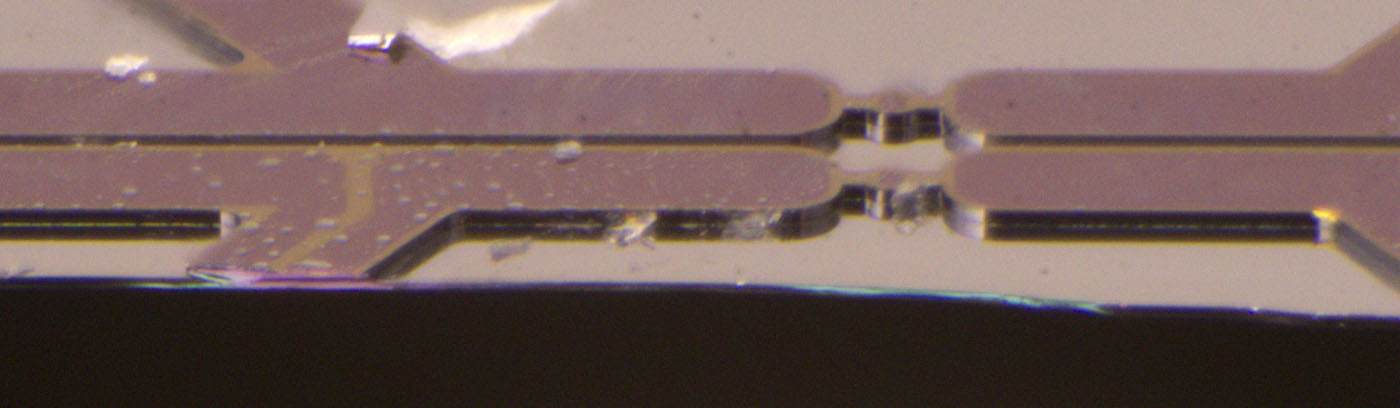


If you destroy the membrane, you can see how thin it is. While the height of the piezoresistive layer is roughly estimated at 20µm, the membrane is not even 10µm thick.
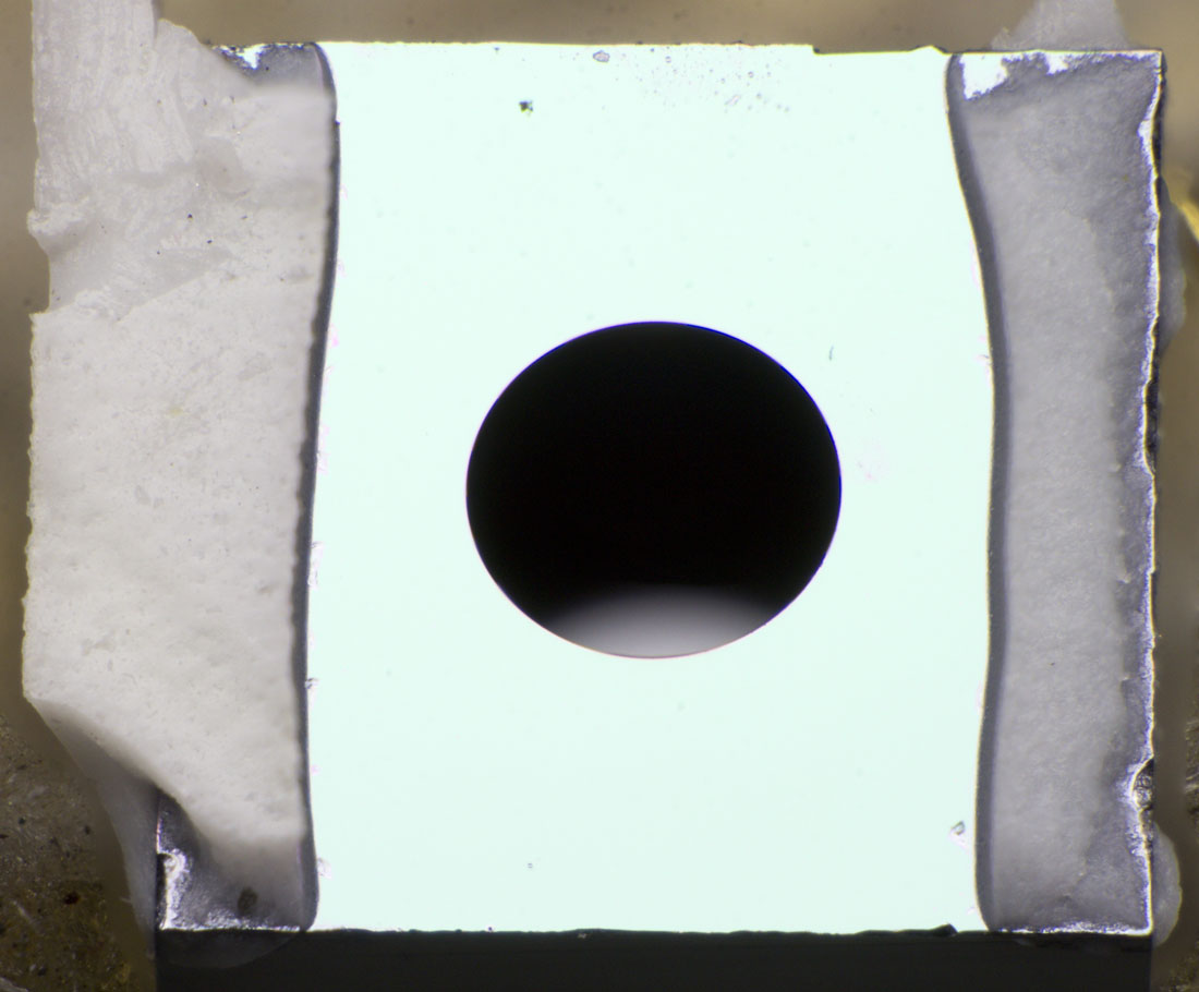


The module has a circular opening on the underside.
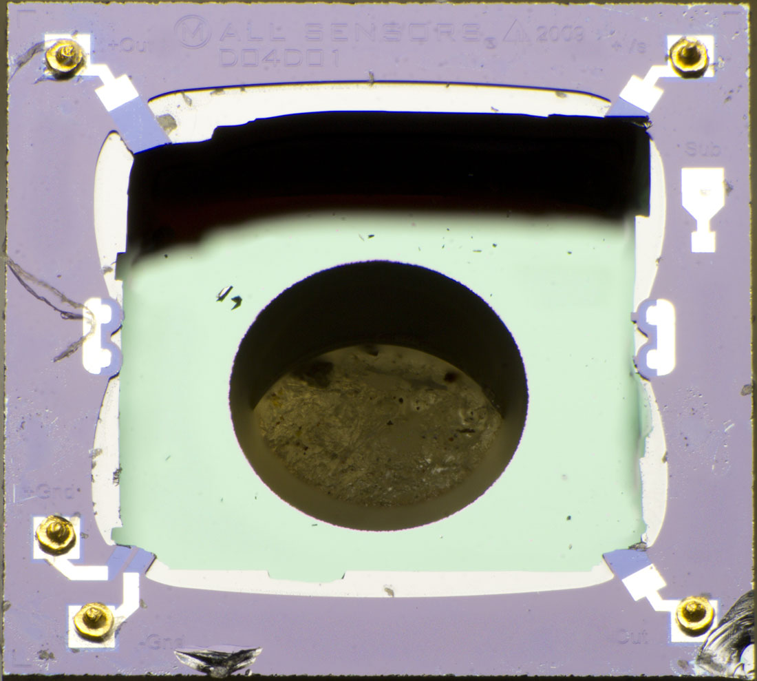


If you remove the membrane completely, you can take a look at the cavity underneath. From the side, it could already be seen that the module consists of two elements. The lower element contains the circular hole, while a larger cavity has been inserted in the upper element.
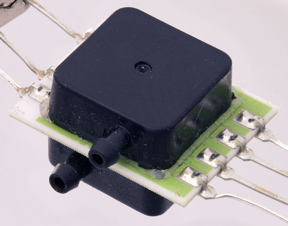


Here you can see an alternative configuration where there is a plastic half-shell with a hose connection on both sides.
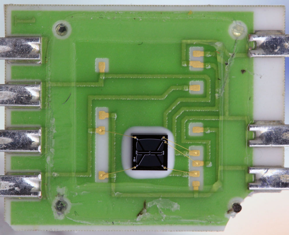
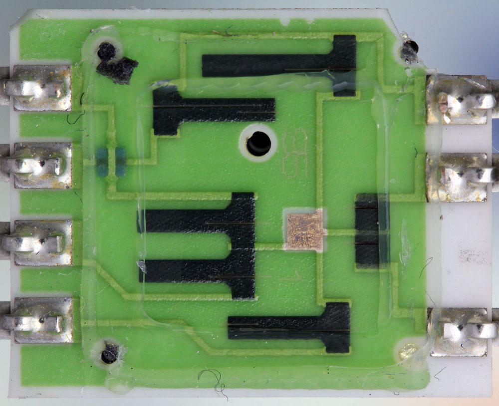


Only one pressure sensor module was used in this component. However, the same ceramic carrier was used as for the first pressure sensor.
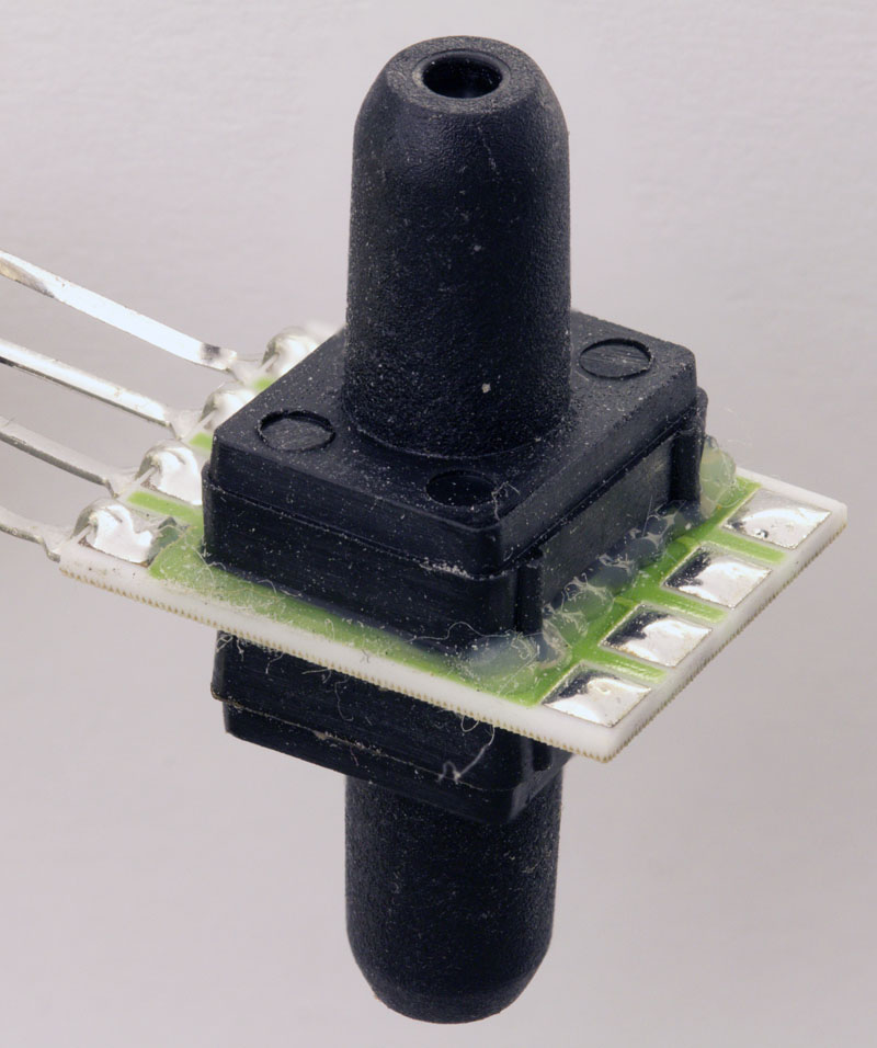


The third pressure sensor variant is somewhat smaller.
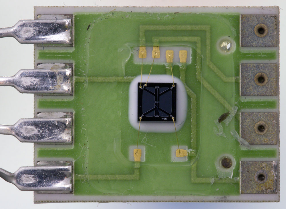


Again, only one sensor module was used.


https://www.richis-lab.de/MEMS_11.htm

 :-/O
 
The following users thanked this post: Gyro, RoGeorge, ch_scr, iMo

Online iMo

  • Super Contributor
  • ***
  • Posts: 6922
  • Country: li
Re: MEMS - nice die pictures
« Reply #30 on: October 18, 2023, 06:44:07 am »
Any idea how the membrane and the hole have been manufactured?
Readers discretion is advised..
 

Offline NoopyTopic starter

  • Super Contributor
  • ***
  • Posts: 2410
  • Country: de
    • Richis-Lab
Re: MEMS - nice die pictures
« Reply #31 on: October 18, 2023, 06:59:22 am »
Any idea how the membrane and the hole have been manufactured?

They do some ething...  ;D

I don´t know the details but the whole MEMS world depends on ething the right materials at the right time in the right direction.
Here in my view it is easier because they do just "normal" etching into two parts and after that bond the two parts together. More complex and small structures need sacrificial layers and more selective etching in more challenging places.

Offline NoopyTopic starter

  • Super Contributor
  • ***
  • Posts: 2410
  • Country: de
    • Richis-Lab
Re: MEMS - nice die pictures
« Reply #32 on: October 05, 2025, 03:25:25 am »


VTI Technologies is a Finnish company that now belongs to Murata. The SCA610 belongs to a family of acceleration sensors. The SCA610-C28H1A measures accelerations in one direction in the range of +/-1.7g. The component offers a self-test and outputs an analog signal.


The package contains the actual acceleration sensor and the evaluation circuit. A silicone gel protects both elements.


Compared to other acceleration sensors, the evaluation circuit is relatively simple in design.

This image is also available in a higher resolution: https://www.richis-lab.de/images/MEMS/14_04XL.jpg (48MB)


The design dates back to 1997. Seven masks can be seen.


The acceleration sensor is surprisingly high at 2,5 mm. It has six contacts on the top, three of which were connected to the evaluation circuit. As will become apparent, these are three potentials that can be contacted on both sides.


It is clear to see that the acceleration sensor was constructed with three elements. The spaces between them appear to be made of glass. The width of the entire structure is 1,9 mm.


Dark elements are visible in the lower part of the transparent areas.


The acceleration sensor operates capacitively. In the center of the package is a spring-mounted mass, which has already broken out here. Metallized surfaces on both sides form two capacitors with the movable mass. The inertia of the mass ensures that it moves out of its central position when accelerated. The two capacitances change accordingly.


The sensor assembly measures 1,8 mm x 1,2 mm and is 0,3 mm thick. The two holes probably optimize air resistance and thus the damping. On one side of the lower edge, a remnant of the mounting can still be seen. The thin strips provide the necessary flexibility.


The remains of the mounting can also be seen on the lower edge of the housing.


The two metal surfaces, which represent the fixed electrodes, are applied on the transparent glass. The dark elements in the glass appear to be the conductive contacts between the electrodes and the external elements. How exactly the contact was made remains unclear. The surface above shows an unusual surface structure.


https://www.richis-lab.de/MEMS_12.htm

 :-/O
 
The following users thanked this post: RoGeorge


Share me

Digg  Facebook  SlashDot  Delicious  Technorati  Twitter  Google  Yahoo
Smf


-->