Author Topic: Opamps - Die pictures  (Read 260306 times)

0 Members and 22 Guests are viewing this topic.

Offline D Straney

  • Frequent Contributor
  • **
  • Posts: 390
  • Country: us
Re: Opamps - Die pictures
« Reply #875 on: April 10, 2026, 02:05:37 am »
Ok, it's "mystery op-amp time" again.  I made a pass through this whole thread rather than relying on my fallible memory this time, to make sure this one hadn't already been discussed ;D  (Was going to take a pass through Zeptobars too, but it seems to be down at the moment???)

These come from a Burr-Brown 3650HG (optical) isolation amplifier, which has 3 identical copies of this op-amp as its only active circuitry.  They seem to fall into a mid-range complexity: there's no laser-trimmed resistors or zener-zap adjustments or chopper circuitry, but it's also not a minimal op-amp like the 709.

The input diff pair lives at the top, and I think they're cascoded with the circular transistors below them, if I'm reading it correctly.  There's also some connections to possibly weird-shaped transistors that I'm not sure about: see both ends of the horizontal trace just above the capacitor.
 
The following users thanked this post: RoGeorge, ch_scr

Online magic

  • Super Contributor
  • ***
  • Posts: 8056
  • Country: pl
Re: Opamps - Die pictures
« Reply #876 on: April 10, 2026, 01:53:04 pm »
NPN emitter followers driving a pair of common base PNPs was state of the art 1960s circuit design.
Collector current of the NPNs mirrored into the bases of the PNPs means it's some 741 variant.
A later one with improved thermal symmetry. I don't know who made it.
 
The following users thanked this post: D Straney

Online AnalogTodd

  • Regular Contributor
  • *
  • Posts: 219
  • Country: us
Re: Opamps - Die pictures
« Reply #877 on: April 10, 2026, 05:12:21 pm »
The input diff pair lives at the top, and I think they're cascoded with the circular transistors below them, if I'm reading it correctly.  There's also some connections to possibly weird-shaped transistors that I'm not sure about: see both ends of the horizontal trace just above the capacitor.
Those connections actually look like they are what we used to use to cross under single layer metal on an old bipolar process. There's contact to a light pink diffusion that sits on top of the tub isolation and runs out to the ground (or V-) line. It's usually a N+ layer doped on top of the P-type isolation and since it is at the same potential (ground or V-) there's not a concern of hitting breakdown or worrying about leakage.
Lived in the home of the gurus for many years.
 
The following users thanked this post: D Straney

Offline NoopyTopic starter

  • Super Contributor
  • ***
  • Posts: 2384
  • Country: de
    • Richis-Lab
Re: Opamps - Die pictures
« Reply #878 on: April 11, 2026, 03:41:44 am »
Ok, it's "mystery op-amp time" again.

I have seen these auxiliary structures and this invers name with revision. Somewhere... But I can´t find the part.


The OPA4134 documented here was purchased from AliExpress. At first glance, the package and the marking appear unremarkable. Upon closer inspection, however, the texture of the indentation at pin 1 seems unusually smooth. Added to this is the shape of the letter B in the logo. On the original, the curves of the letter are all the same length.


It is immediately apparent that this is not an OPA4134. The die has a edge length of just 1,1mm.

There are four opamps on the die. The manufacturer is unclear. Only the character strings 20 or 02 and 324 are visible in the center of the die. A nice detail is the + and ground symbols on the power supply bondpads.

This image is also available in higher resolution: https://www.richis-lab.de/images/Opamp/a27x02XL.jpg (14MB)


It is clearly an LM324. That explains the number sequence 324.


https://www.richis-lab.de/OpampA22.htm

 :-/O
 
The following users thanked this post: RoGeorge, D Straney

Offline NoopyTopic starter

  • Super Contributor
  • ***
  • Posts: 2384
  • Country: de
    • Richis-Lab
Re: Opamps - Die pictures
« Reply #879 on: April 27, 2026, 03:17:45 am »


One more LM2904!  ;D

This one was purchased from Mouser as the Texas Instruments LM2904N. As already mentioned the “N” refers to the LM2904 variant from National Semiconductor. Texas Instruments acquired National Semiconductor and continues to offer their variant. The device actually still bears the National Semiconductor logo.


The die measures 1,2mm x 0,9mm. The letters “UK” in the upper right corner indicate that it was developed or manufactured in the United Kingdom. The marking on the left edge indicates that this LM2904 is also based on the LM158 design. It appears to be Revision D. The circuit has not changed compared to Revision C (https://www.richis-lab.de/HDD_WD_Caviar_22500.htm#LM358). The geometries of the individual elements differ slightly, and in some cases, their placement is minimally different.

This image is also available in higher resolution: https://www.richis-lab.de/images/Opamp/a28x02XL.jpg (13MB)


In the center of the die is a National Semiconductor logo. To the left and right of it are the revision numbers of five masks.


The circuit corresponds to the circuit in the Texas Instruments LM2904.


Since not everybody has recogniced it in the first place: Transistors Q2 and Q4 divert a large portion of their emitter current to Vcc-. On the die, this is done within one transistor structure. A small collector is connected to the current mirror (yellow). The remainder of the emitter consists of a p-doped region connected to the isolation frame connected to Vcc-. A large portion of the emitter current is dissipated in this region (purple).


https://www.richis-lab.de/OpampA23.htm

 :-/O
 
The following users thanked this post: RoGeorge, ch_scr, magic, D Straney, mawyatt

Online magic

  • Super Contributor
  • ***
  • Posts: 8056
  • Country: pl
Re: Opamps - Die pictures
« Reply #880 on: April 27, 2026, 04:18:35 am »
This one was purchased from Mouser as the Texas Instruments LM2904N. As already mentioned the “N” refers to the LM2904 variant from National Semiconductor. Texas Instruments acquired National Semiconductor and continues to offer their variant. The device actually still bears the National Semiconductor logo.
Nice to see that they still haven't replaced it with CMOS ;D
Pin 1 marking style is TI, so they package them together with their own chips now.

Are you sure that UK means UK? National was a US company.
I have also seen UK on LM336.
And I have seen NSUK on LM4562, LM3915.
 

Offline NoopyTopic starter

  • Super Contributor
  • ***
  • Posts: 2384
  • Country: de
    • Richis-Lab
Re: Opamps - Die pictures
« Reply #881 on: April 27, 2026, 04:34:13 am »
Are you sure that UK means UK? National was a US company.
I have also seen UK on LM336.
And I have seen NSUK on LM4562, LM3915.

I'm not 100% sure but National Semiconductor produced quite some analog circuits in UK:
https://www.glassdoor.co.uk/Overview/Working-at-National-Semiconductor-UK-EI_IE36966.11,36.htm

Offline mkmk!

  • Newbie
  • Posts: 1
  • Country: gr
Re: Opamps - Die pictures
« Reply #882 on: June 12, 2026, 05:04:55 pm »
Hello,
just for curiosity, i opened a ne5532 from the new ones (2026) and the die looks identical to TL6113 mentioned above. Sorry i don t post pictures, they are not clear.
 
The following users thanked this post: Doctorandus_P, Noopy

Offline NoopyTopic starter

  • Super Contributor
  • ***
  • Posts: 2384
  • Country: de
    • Richis-Lab
Re: Opamps - Die pictures
« Reply #883 on: July 22, 2026, 03:21:20 am »


The part documented here is manufactured by Fairchild and is designated µ3A770931. The package is known as a flat pack and is typically used in military and aerospace applications.


The designation µ3A770931 or U3A770931 cannot be easily identified. The “Fairchild Semiconductor Integrated Circuit Data Catalog” from 1970 lists a U3F7709311 and a U3F7709312 and explains how the designations are structured. The package family 3 lists several flat packages. However, a 3A variant is not mentioned there. 7709 indicates that it is a µA709. The operating temperature range 31 extends from -55°C to +125°C.


The edge length is 1,4mm. The design differs somewhat from the 1987 design. However, the circuit is essentially the same.

This image is also available in a higher resolution: https://www.richis-lab.de/images/Opamp/a29x06XL.jpg (18MB)


https://www.richis-lab.de/OpampA24.htm

 :-/O
 
The following users thanked this post: RoGeorge, ch_scr, D Straney

Offline exe

  • Supporter
  • ****
  • Posts: 2991
  • Country: nl
  • self-educated hobbyist
Re: Opamps - Die pictures
« Reply #884 on: July 22, 2026, 06:30:28 am »
Was the metal layer mask hand-drawn? Wait, the whole chip is probably hand-drawn?
 

Offline NoopyTopic starter

  • Super Contributor
  • ***
  • Posts: 2384
  • Country: de
    • Richis-Lab
Re: Opamps - Die pictures
« Reply #885 on: July 22, 2026, 01:57:30 pm »
As far as I know they used a special tape to "draw" the geometries they needed. Back then that was a very manual process.

Online AnalogTodd

  • Regular Contributor
  • *
  • Posts: 219
  • Country: us
Re: Opamps - Die pictures
« Reply #886 on: July 22, 2026, 02:11:00 pm »
As far as I know they used a special tape to "draw" the geometries they needed. Back then that was a very manual process.
Rubylith layout process. VERY tedious, I never had to work with it though I have seen old rubylith stencils in my years of doing IC design and layout. They were kept in case things needed to be updated, at which point they would actually digitize the layout and then do the re-work. I started when we still used color keys to check layouts between release from our layout group and prior to mask generation. Watched us go from there to 'fractured' data, then to just digital JDV (job deck view) on screen.

More info: https://en.wikipedia.org/wiki/Rubylith
Lived in the home of the gurus for many years.
 
The following users thanked this post: RoGeorge, Noopy

Offline NoopyTopic starter

  • Super Contributor
  • ***
  • Posts: 2384
  • Country: de
    • Richis-Lab
Re: Opamps - Die pictures
« Reply #887 on: September 07, 2026, 03:10:56 am »


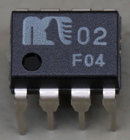
The MUSES02 is a dual opamp optimized for high-end audio applications. It was developed by the Japanese company New Japan Radio. It is now part of Nisshinbo Micro Devices, a joint venture between New Japan Radio and Ricoh Electronic Devices. Digi-Key offers the MUSES02 at a unit price of 56€.

The operating voltage range extends from ±3,5V to ±16V. The typical current consumption is 8mA. The datasheet prominently highlights the noise voltage density of 4,5nV/√Hz and the voltage gain of 110 dB. The maximum voltage rise time is typically 5 V/µs. The bandwidth is specified at 5,8MHz. The manufacturer guarantees isolation with an attenuation of 150dB between the two integrated opamps. Changes in common-mode voltage and supply voltage are typically attenuated by 110dB.
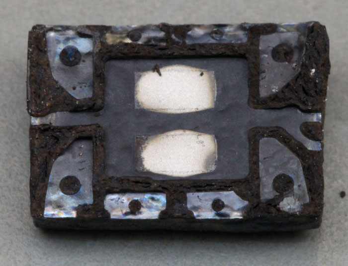


The two opamps are located on two separate dies. This explains the low crosstalk from one side to the other.
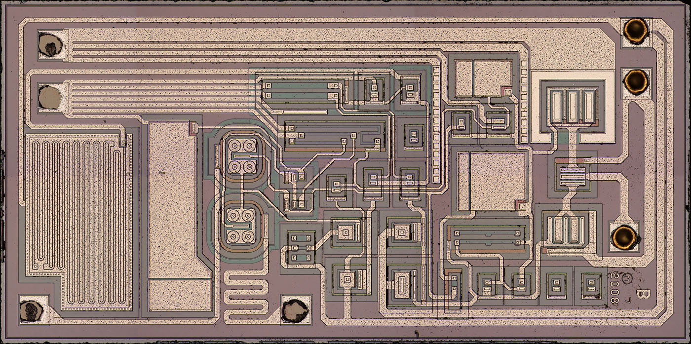


The die measures 2,5mm x 1,2mm. The process does not appear to be particularly advanced. The structures are relatively large, and there are no special elements. Large structures are definitely an advantage in the field of precision circuits. For example, larger elements inherently generate less noise.

This image is also available in a higher resolution: https://www.richis-lab.de/images/Opamp/a30x03XL.jpg (36MB)
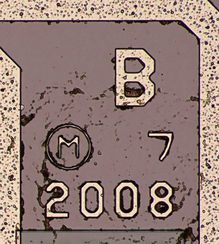


The design appears to date from 2008. The letter B could stand for a second revision, but it could also have a different meaning. The symbol, which resembles the number 7, is often found on components from Nisshinbo Micro Devices. Its meaning remains unclear.
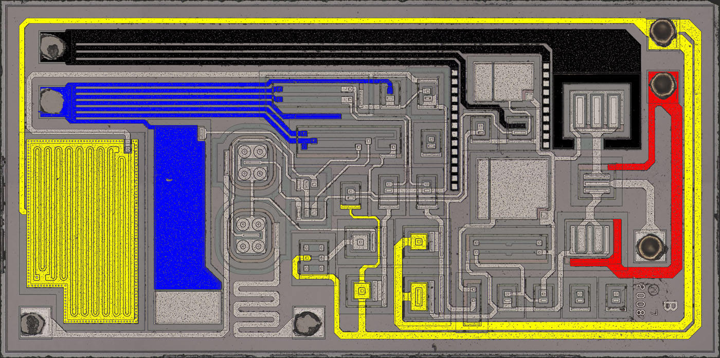


If you take a closer look at the circuit, you’ll notice that a great deal of effort went into the power supply. Both the negative and positive potentials are routed via two bondwires each to different bondpads. In addition, the potentials have been distributed in a star configuration from these bondpads so that the individual circuit blocks interfere with each other as little as possible.
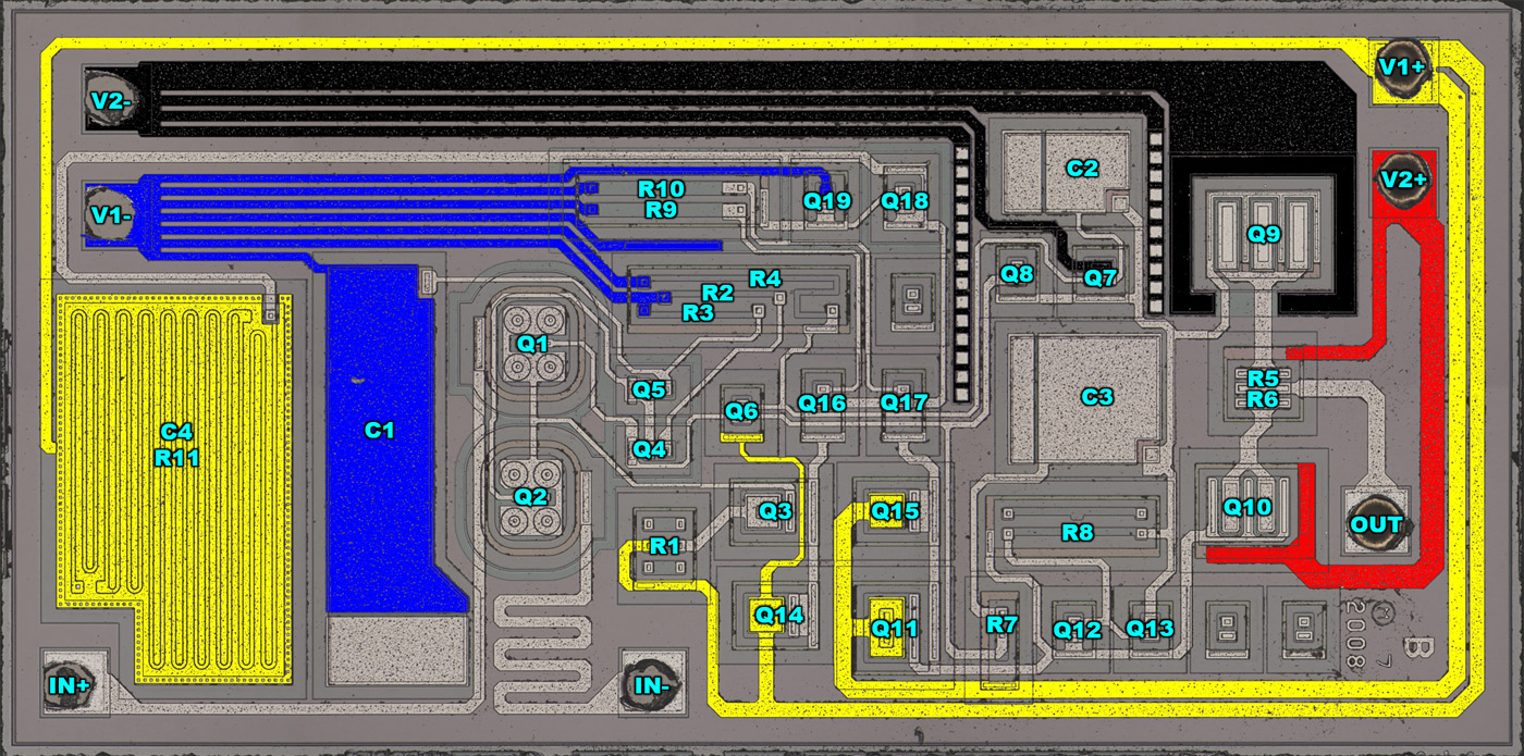
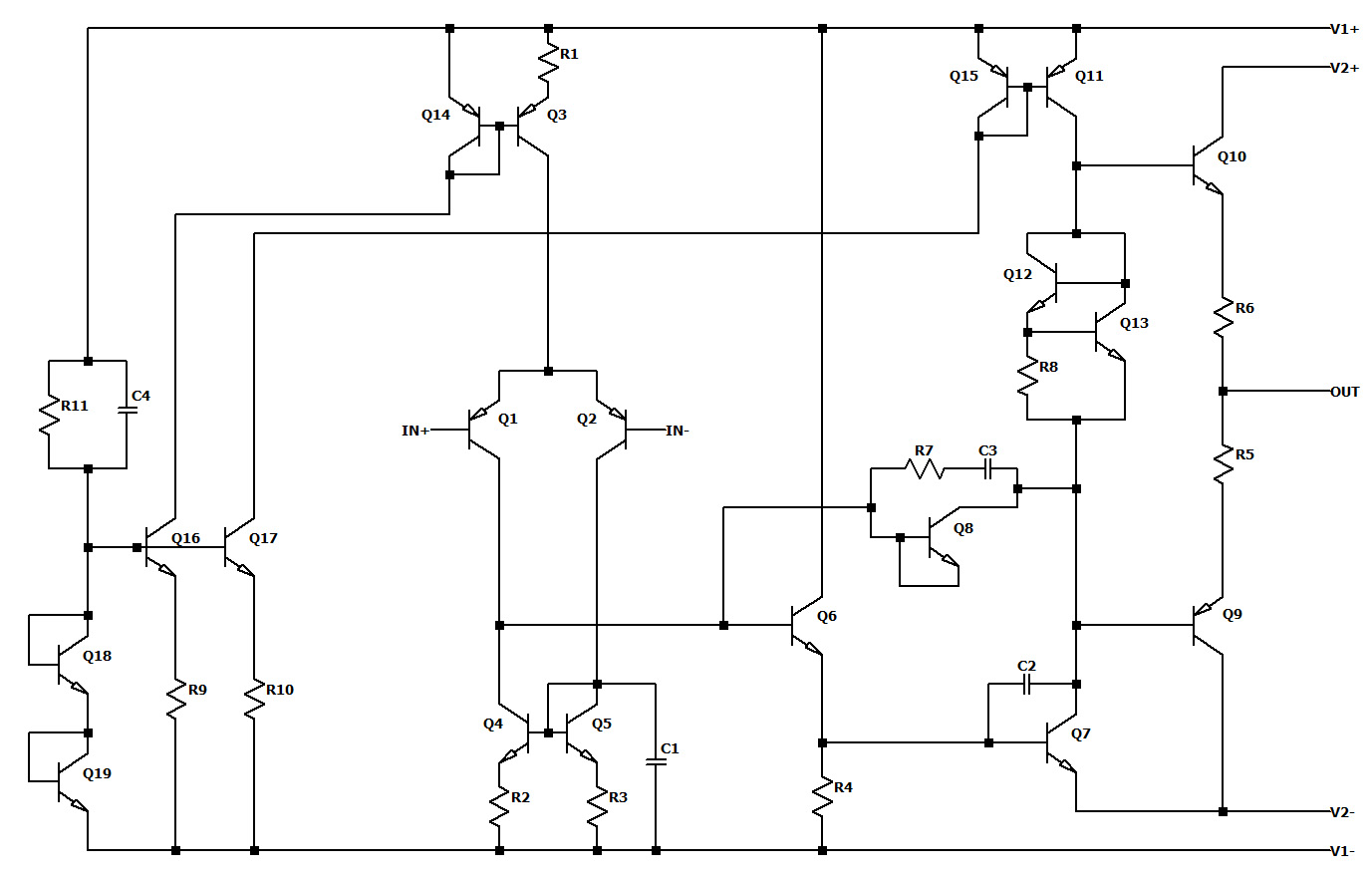


The integrated circuit is not overly complex, but it does have a few unique features. Two PNP transistors, embedded in a classic differential amplifier, serve as the input stage. The traces from the bondpads to the input transistors are designed to be of equal length and thus have equal resistance. The transistor pairs Q1/Q2 and Q4/Q5 have been placed roughly in the center and in a crisscross pattern. Both measures reduce the influence of thermal gradients on the input stage.

Transistor Q6 acts as a buffer stage that reduces the unbalanced load on the differential amplifier caused by the subsequent amplifier stage. Transistor Q7 provides the voltage gain of the opamp. The voltage amplifier stage and the output stage use the second negative potential V2-, so that their dynamic currents do not affect the potential V1-. The voltage amplifier is powered by a constant current supplied via transistor Q11. Since the operating current is constant, the potential V1+ can be used for this purpose.

The Capacitor C2 reduces the effect of the base-collector capacitance of transistor Q7. This so-called Miller capacitance is voltage-dependent and can distort the signal accordingly. (I know most of you know the topic but sometimes there are newbis in the room.) C2 also limits the frequency response of the opamp. The RC network R7/C3 provides additional local negative feedback. Transistor Q8 protects the output stage from overload. If Q7 is driven to the point where its collector potential drops significantly, Q8 turns on and draws base current from Q6, which ultimately reduces the drive level of the chain all the way to Q9.

The Q12/R8/Q13 block generates a specific voltage drop that ensures both output stage transistors always allow a certain amount of quiescent current to flow in the crossover region. This reduces crossover distortion at the signal’s zero-crossing point. The output stage is configured in a complementary configuration. The two paths are combined via two low-impedance resistors.

The control of the two current sources, Q3 and Q11, is unusual. It is not achieved via a common bias potential. Each current source has its own current mirror, which gets its reference current from its own current sink. Clearly, great care was taken to isolate the current sources from one another as much as possible. In contrast, the control of current sources Q16 and Q17 is designed to be relatively simple. The reference voltage on which the currents are based is generated by the two base-emitter paths of transistors Q18 and Q19. Their operating current is set solely via resistor R11. Capacitor C4 acts as a stabilizer against high-frequency disturbances in the power supply. It is located on the resistor loops and is thus, strictly speaking, distributed across the resistor. The significant influence of temperature on the voltage drop across transistors Q18 and Q19—and thus on the operating currents—remain uncompensated.

The MUSES02 contains several variable and optional elements. The operating current of the differential amplifier can be adjusted via the three elements of resistor R1. The capacitance of C1 can also be adjusted via the metal layer. It limits the frequency response of the differential amplifier. Similarly, the frequency response of the opamp can be influenced via the metal surface of capacitors C2 and C3. A second, unused resistor is connected in parallel with R8. Both strips have a widening in the center that could be used as a contact area. This can be used to vary the quiescent current of the output stage. To the right of transistor Q13 are two unused transistors. Perhaps these transistors were intended to allow for a different configuration of the quiescent current setting. The reference currents of the current sources can also be adjusted extensively. Resistor R11 has two optional contacts. Above transistor Q18 is another transistor that could be used to increase the reference voltage by one additional base-emitter voltage drop. Less obvious are the extended contacts on resistors R9 and R10. These can also be used to slightly vary the currents in the differential amplifier and in the voltage amplification stage.
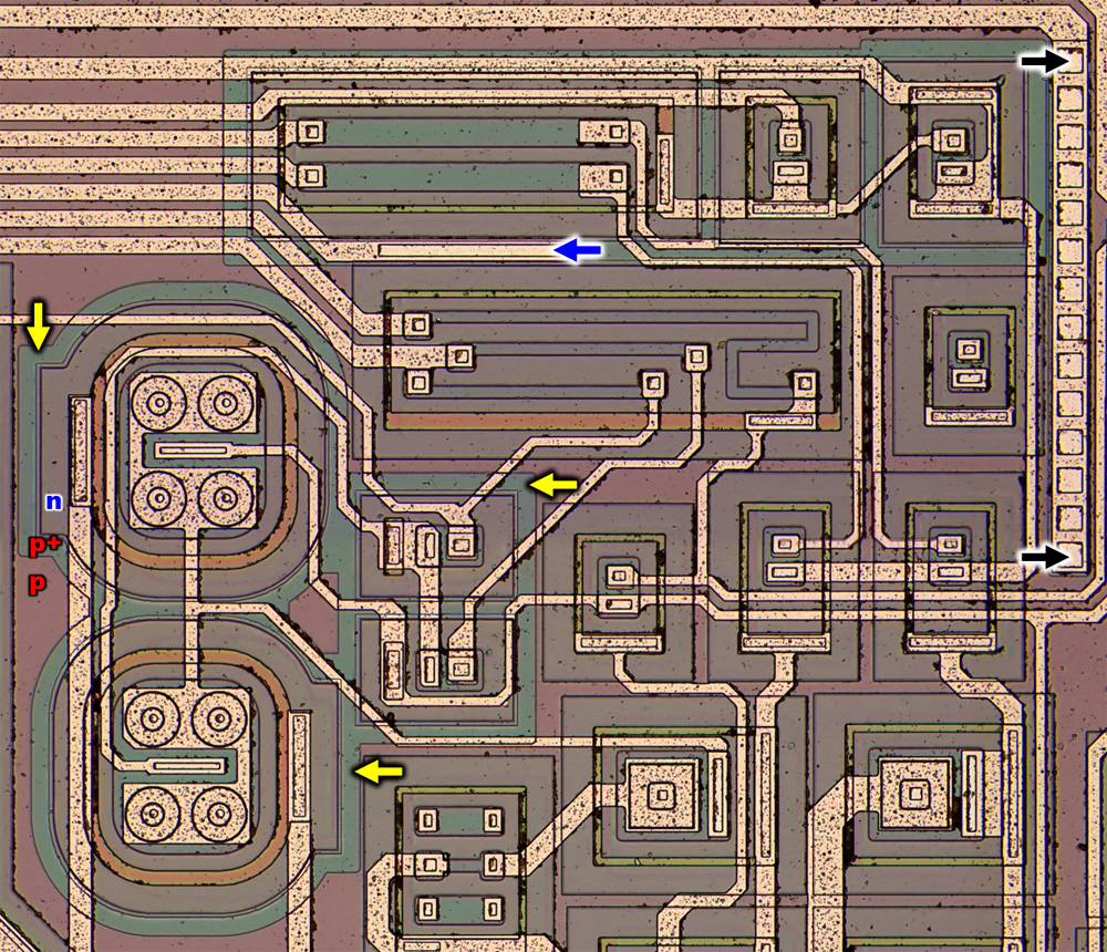


The substrate of the MUSES02 is p doped. It is accordingly connected to the negative supply potential (black). The two elongated contacts have been deliberately placed next to the output stage and next to the voltage amplifier. The transistors and resistors are located in n-type wells and are thus isolated from one another. The differential section of the differential amplifier has an additional, wider frame (yellow). Additional p-doping has apparently been introduced there. A similar frame is found in the bias section. There, the frame is additionally connected to the less-loaded negative supply potential (blue). It remains unclear why the frame of the differential amplifier was not connected in the same way. Nevertheless, the frame has a balancing effect on the local substrate potential.


https://www.richis-lab.de/OpampA25.htm

 :-/O
 
The following users thanked this post: exe, RoGeorge, magic, D Straney, AnalogTodd, MT4S301


Share me

Digg  Facebook  SlashDot  Delicious  Technorati  Twitter  Google  Yahoo
Smf