Well, at least there is some truth in this. I'm still not sure I want to pay for this.
I'd say the circuit is decent, but not outstanding and not worth so much money.

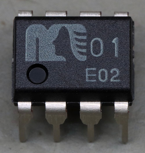
The MUSES01 is the other dual operational amplifier optimized for the high-end audio sector. Digikey offers the MUSES02 at a unit price of €39 for a purchase of 2,000 units.
The operating voltage range extends from ±9V to ±16V. The typical current consumption is 8,5mA. Unlike the MUSES02, the MUSES01 features a JFET input stage. Accordingly, the noise voltage density is noticeably higher at 9.5nV/√Hz. In contrast, the bias current is nearly three orders of magnitude smaller at 200pA. The maximum slew rate is typically 12V/µs, which is significantly higher than that of the MUSES02. The bandwidth, however, is noticeably lower at 3MHz. The manufacturer guarantees isolation between the two integrated operational amplifiers with an attenuation of 150 dB. Changes in common-mode voltage and supply voltage are typically attenuated by 75dB and 83dB, respectively, which is significantly worse than with the MUSES02.
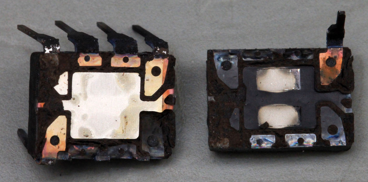
As with the MUSES02, the two opamps are located on two separate dies. This explains the low crosstalk from one side to the other.
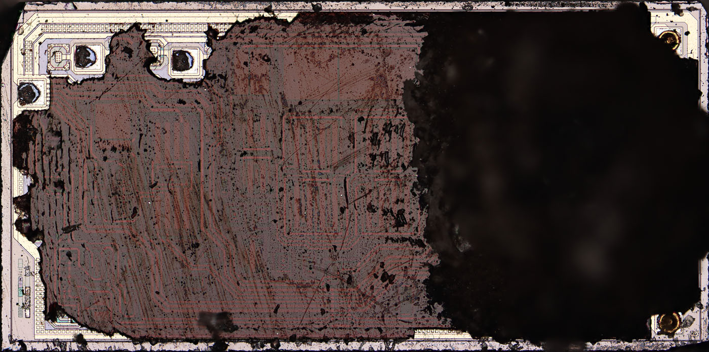
The circuit is coated with a protective polyimide layer.
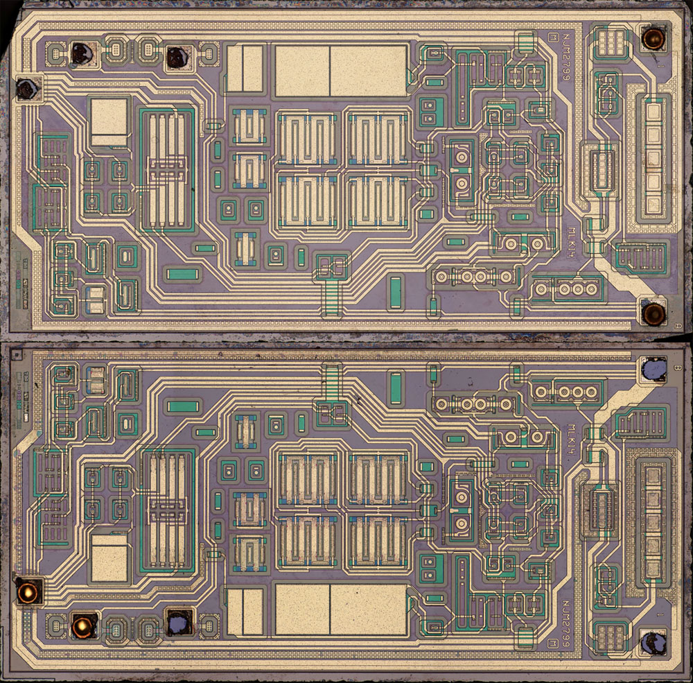
As with the MUSES02, the design has been mirrored so that the bondpads can be properly connected to their corresponding pins.
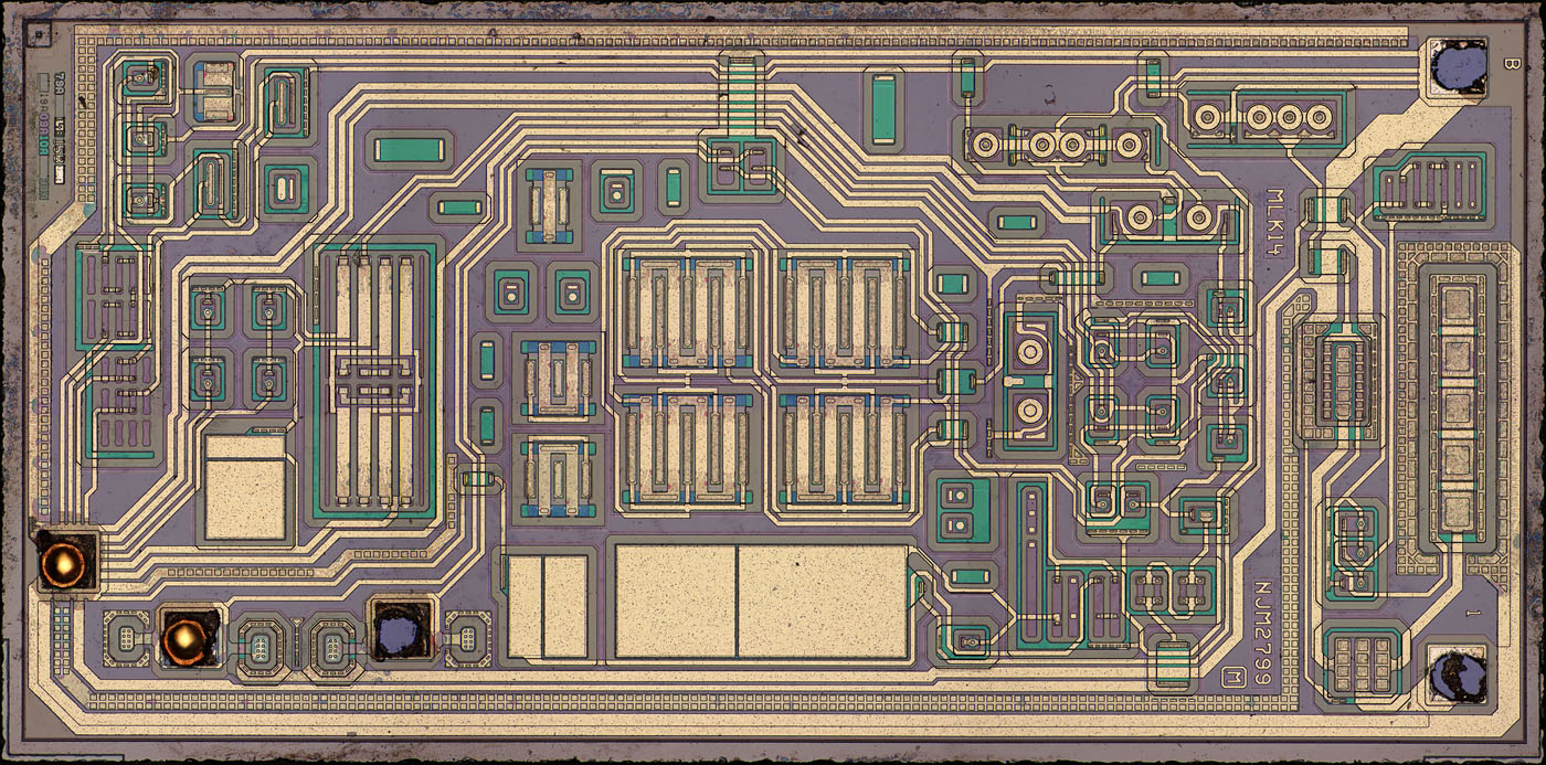
The die measures 2,7mm x 1,3mm. Even without a more detailed analysis of the circuit, it is already clear that the sensitive circuit components and the output stage are arranged around a horizontal axis of symmetry.
This image is also available in a higher resolution:
https://www.richis-lab.de/images/Opamp/a34x04XL.jpg (43MB)

The chip bears the string “NJM2799,” a type designation typical of Nisshinbo Micro Devices. The string “MLK14” cannot be identified. It could be related to a developer or to the manufacturing process.
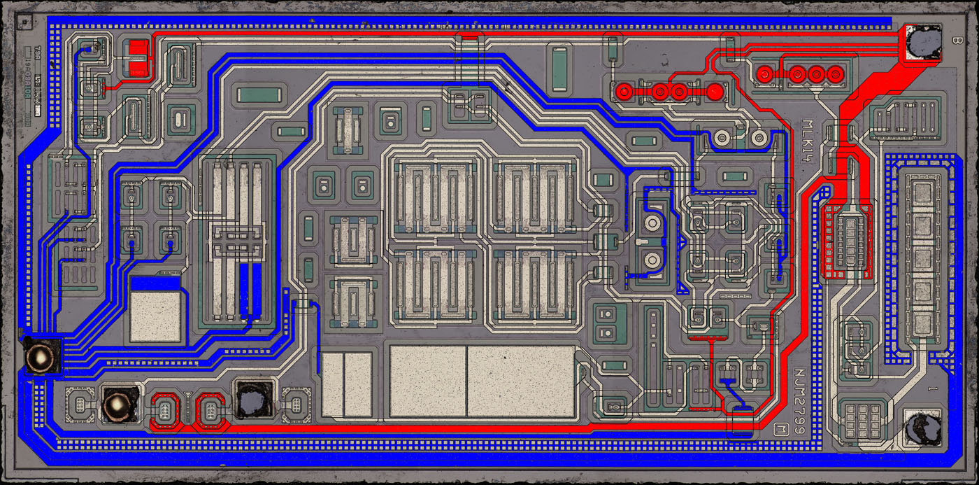
Unlike the MUSES02, the MUSES01 has only one bondpad for each supply voltage. Nevertheless, great effort was made to ensure the best possible power supply. Many circuit components use dedicated traces that radiate in a star pattern to the corresponding bondpad. The negative potential is connected to the substrate all the way around the perimeter. The output stage area (on the right) is shielded with an additional contact strip. A similar strip can be found in the lower left area. There, it was likely the protective structures of the inputs that were being shielded.
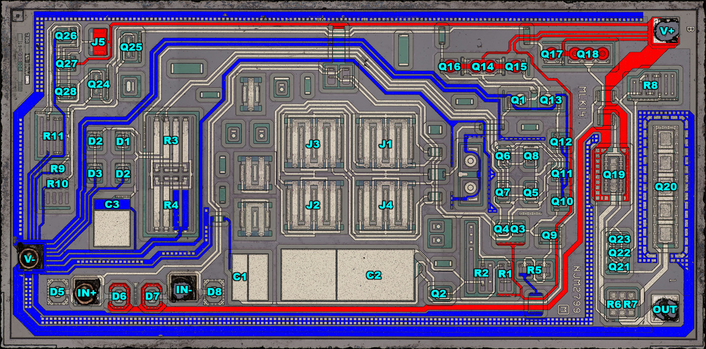
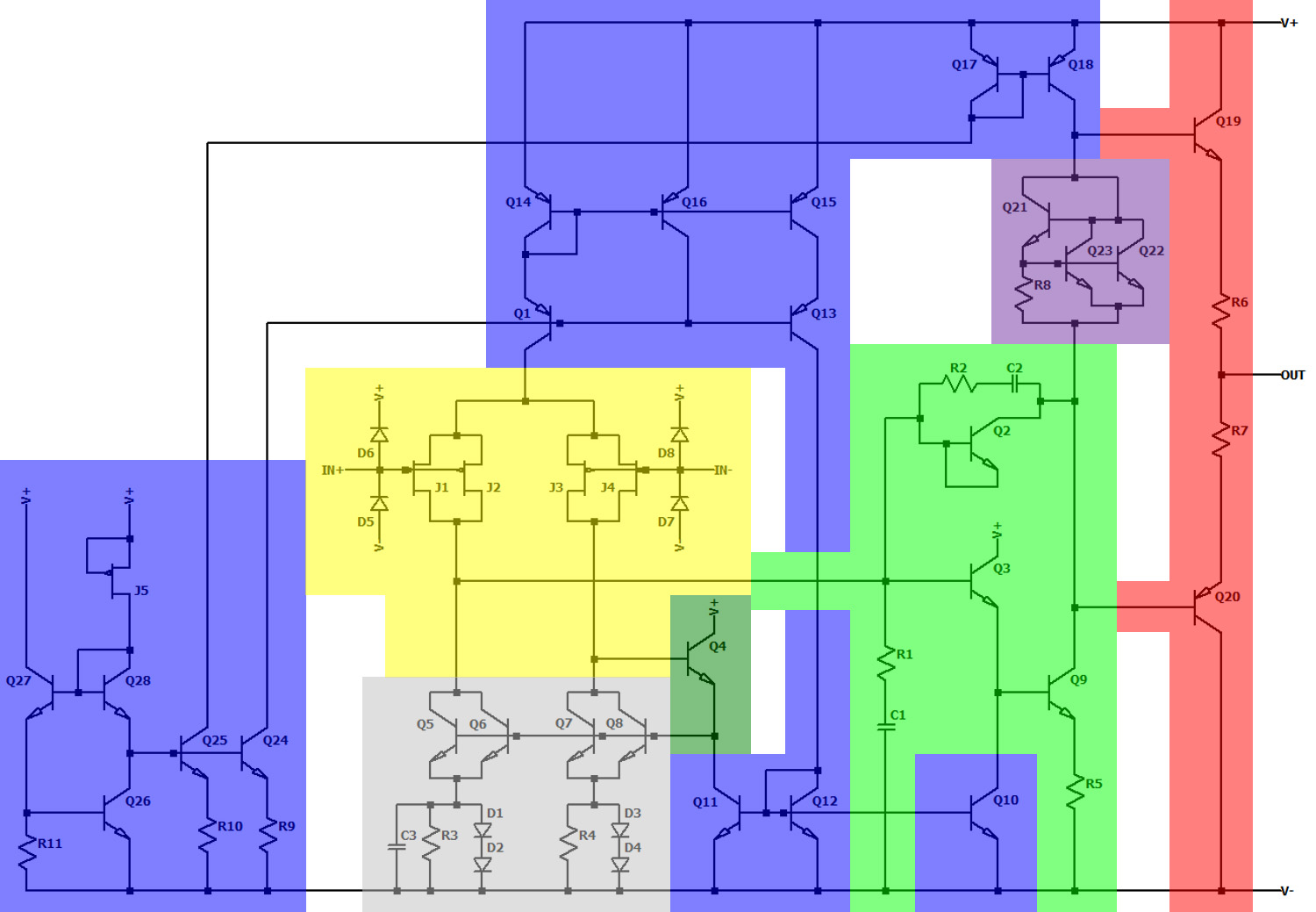
The input of the MUSES01 consists of a differential amplifier with four JFETs (yellow). These input transistors are cross-connected to minimize the influence of temperature gradients. Protective diodes connecting to the two supply voltages are located directly at the input. The differential amplifier is flanked by the current source Q1 and a special current mirror (gray).
The current mirror is special in several respects. These transistors, too, have been duplicated and cross-connected. Like the input transistors and the output stage, the transistor block is located in a straight line in the center of the die. Transistor Q4 (dark green) supplies the necessary base current for the current mirror. However, it has been expanded with a current sink, so that it behaves similarly to the voltage amplifier stage (light green). This ensures that the differential amplifier is loaded as symmetrically as possible. Capacitor C3 limits the frequency response. Diodes D1–D4 limit the voltage across the resistors. This is likely intended to suppress saturation effects.
The differential amplifier is followed by a voltage amplification stage (light green). Transistor Q3 operates with Q10 as the driver stage. The actual voltage amplification takes place in transistor Q9. The compensation capacitor C2 bypasses the amplifier stage Q7/Q9. Additionally, the frequency response is limited by the RC circuit R1/C1. Transistor Q2 likely serves as overload protection for the output stage, as in the MUSES02.
The voltage amplifier stage also serves as the driver stage for the output stage. Three transistors (purple) generate a defined voltage drop, thereby ensuring a certain quiescent current in the output stage. The output stage itself consists of an NPN and a PNP transistor, each equipped with an emitter resistor.
The bias currents (blue) are based on a reference circuit that is slightly more complex than in the MUSES02. However, here as well, two separate current sinks control two distinct regions. The current source for the output stage driver is controlled independently of the rest of the opamp. In the input stage, the two current sources Q1 and Q13 have been expanded to include transistors Q14–Q16.
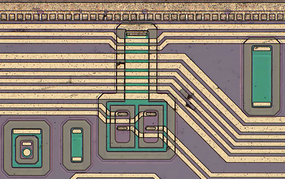
In the traces between the input bondpads and the input transistors, there are two short strips that look like cross-connections. In fact, however, a conscious decision was made to use base doping (purple) there, which has a higher resistance than the collector connections (cyan). Apparently, the design intended to introduce a certain amount of resistance into the gate line. This could be a noise-reduction measure, such as the one explicitly advertised for the Texas Instruments LM2904B (
https://www.richis-lab.de/Opamp94.htm).
https://www.richis-lab.de/OpampA29.htm 

 Home
Home Help
Help Search
 Login
Login Register


 Topic: Opamps - Die pictures (Read 283437 times)

 -->
-->