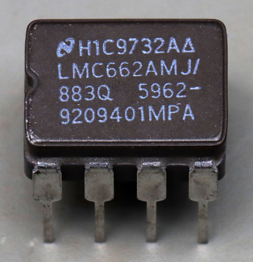
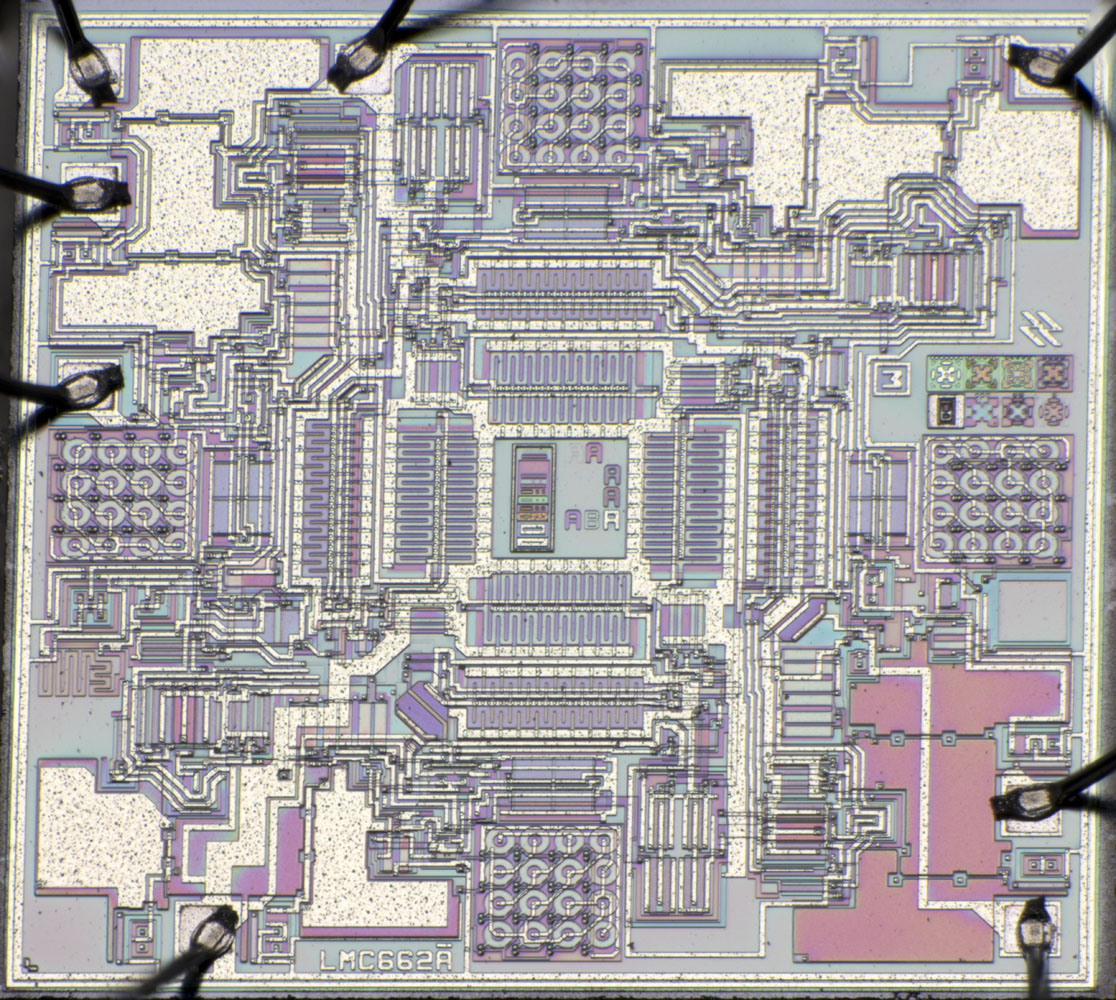
You wanted to see the LMC662? Well, here it is!

The LMC662 is a dual operational amplifier with respectable specifications. The LMC662AMJ variant here is approved for a temperature range of -55°C to +125°C. As will become apparent, the LMC662 is based on the LMC660 quad operational amplifier.
The LMC662 needs just a single supply between 5V and 15V. The current consumption is less than 0,75mA. The input voltage range includes the negative supply. The output is rail to rail. Depending on the operating point, the output stage allows currents up to 40mA. With a slewrate of 1,1V/µs, the LMC662 achieves a cutoff frequency of 1,4MHz.
The extremely low bias current of typically 2fA is achieved by a CMOS input stage. Nevertheless, the noise voltage is quite low at 22nV/√Hz. The current noise is 0,2fA/√Hz. The offset voltage is typically 1mV with a temperature drift of 1,3µV/°C.
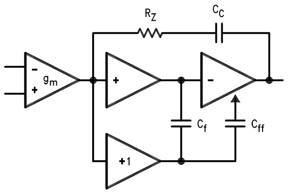
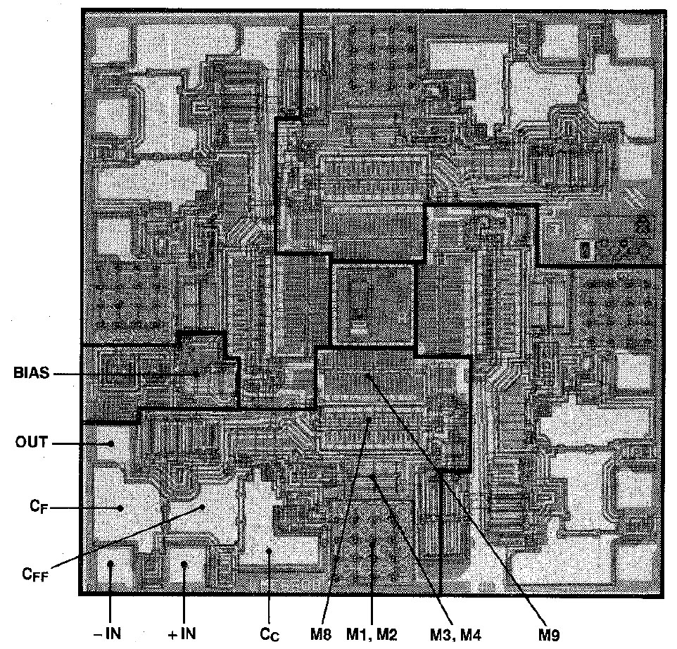
In the datasheet of the LMC662, National Semiconductor shows the somewhat unusual structure of the LMC662. The differential amplifier at the input is followed by a voltage amplifier stage consisting of a non-inverting and an inverting amplifier. Above this voltage amplifier stage is the compensation capacitor Cc. A buffer amplifier drives two capacitors which do some feed forward in the voltage amplifier stage. The LMC662 does not have a classical output buffer stage.
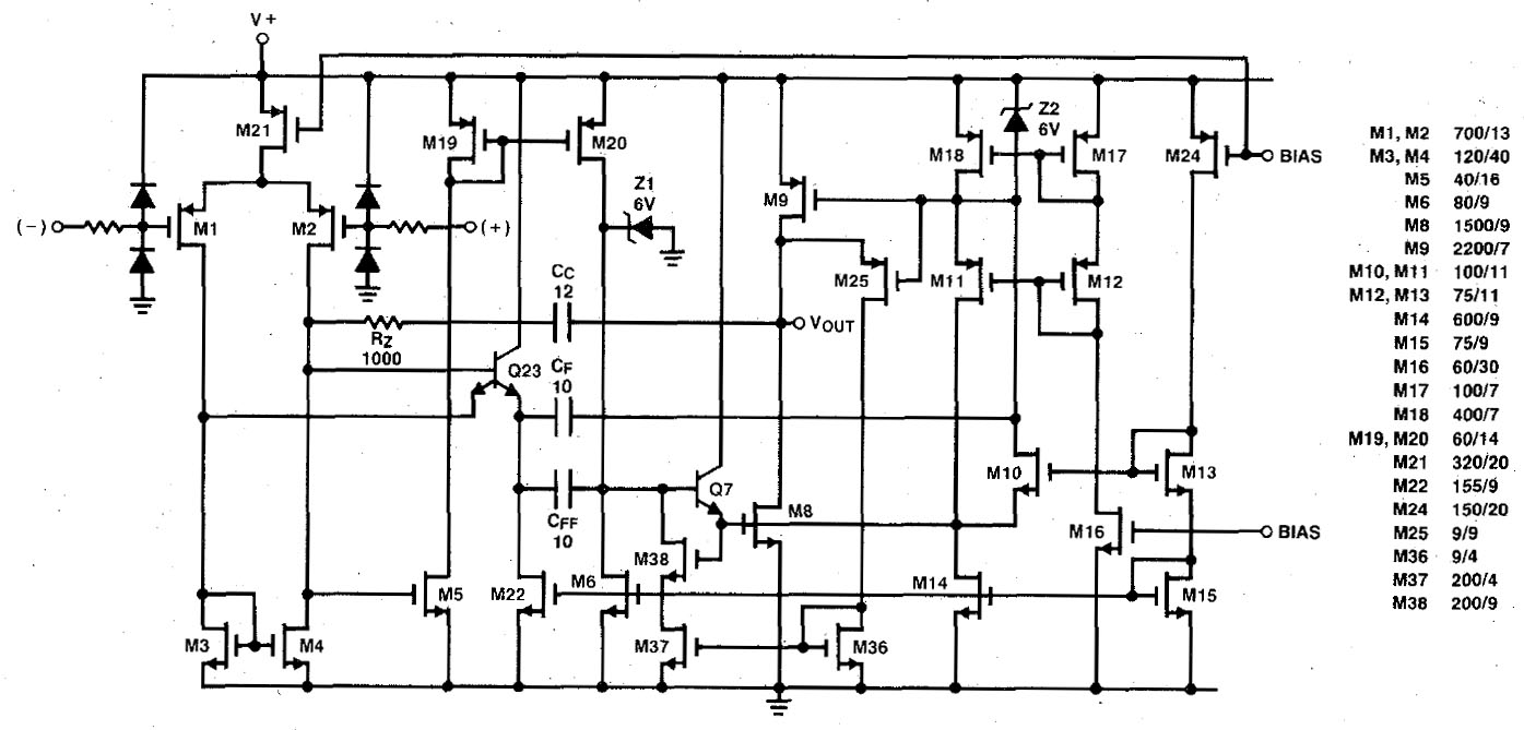
Dennis M. Monticelli describes the LMC662 in great detail in the IEEE article "A Quad CMOS Single-Supply Op Amp with Rail-to-Rail Output Swing". The complete circuit including the layout of the individual transistors is shown there.
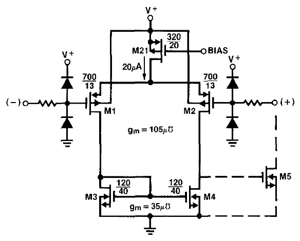
The differential amplifier at the input is classically constructed with a current source and a current mirror. The IEEE paper explains that p-channel MOSFETs without additional threshold doping were used as input transistors. This type of MOSFET would have the least noise.
The LMC662 does not provide a way to adjust the offset voltage, not even after production. Nevertheless, the values for offset voltage and drift are quite good.
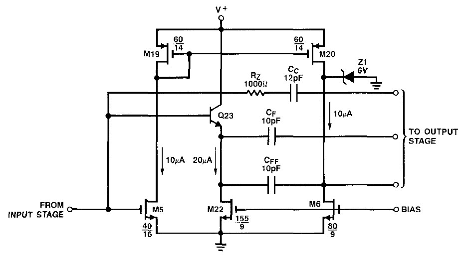
The transistors M5, M19, M20 and M6 amplify the output signal of the differential amplifier and thus drive the output stage. The IEEE paper specifies a gain factor of 40dB. Z1 limits the voltage and thus the current at the output of the LMC662.
Q23 and M22 represent the amplifier stage driving the feedforward capacitors. Cff is connected to the output of the amplifier stage seen here. Cf leads to the output stage.
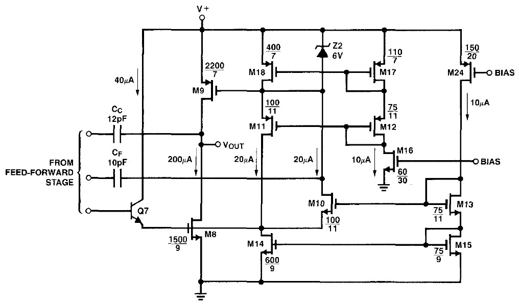
Transistor Q7 provides the driver for the M8/M9 push-pull output stage. According to the IEEE paper, the complex bias circuit ensures that the quiescent current of the output stage does not vary with supply voltage and process variations.
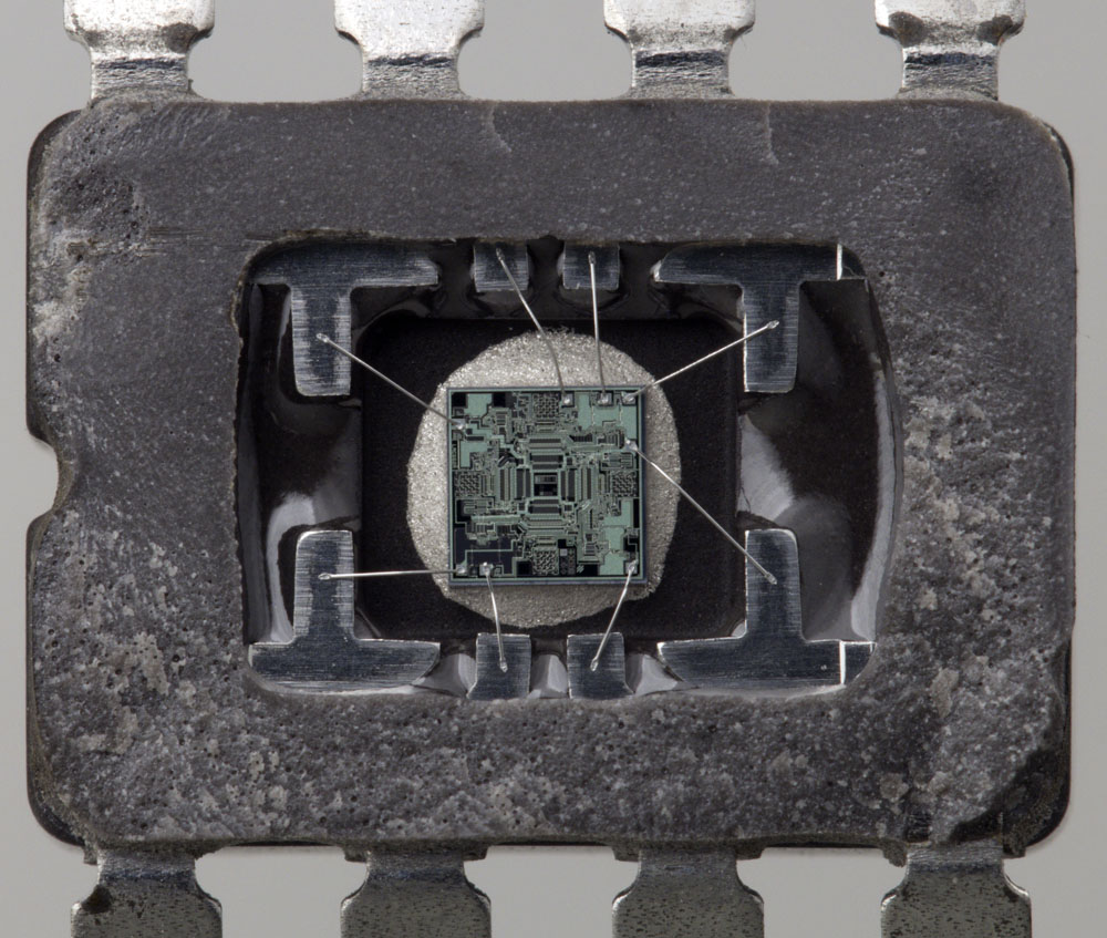
The LMC662AMJ variant, which is specified for the maximum temperature range, is shipped in a ceramic housing.
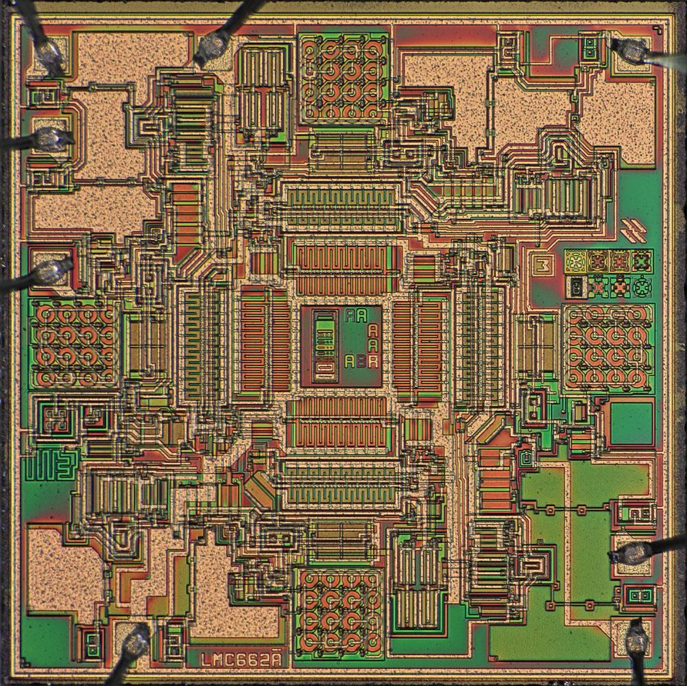
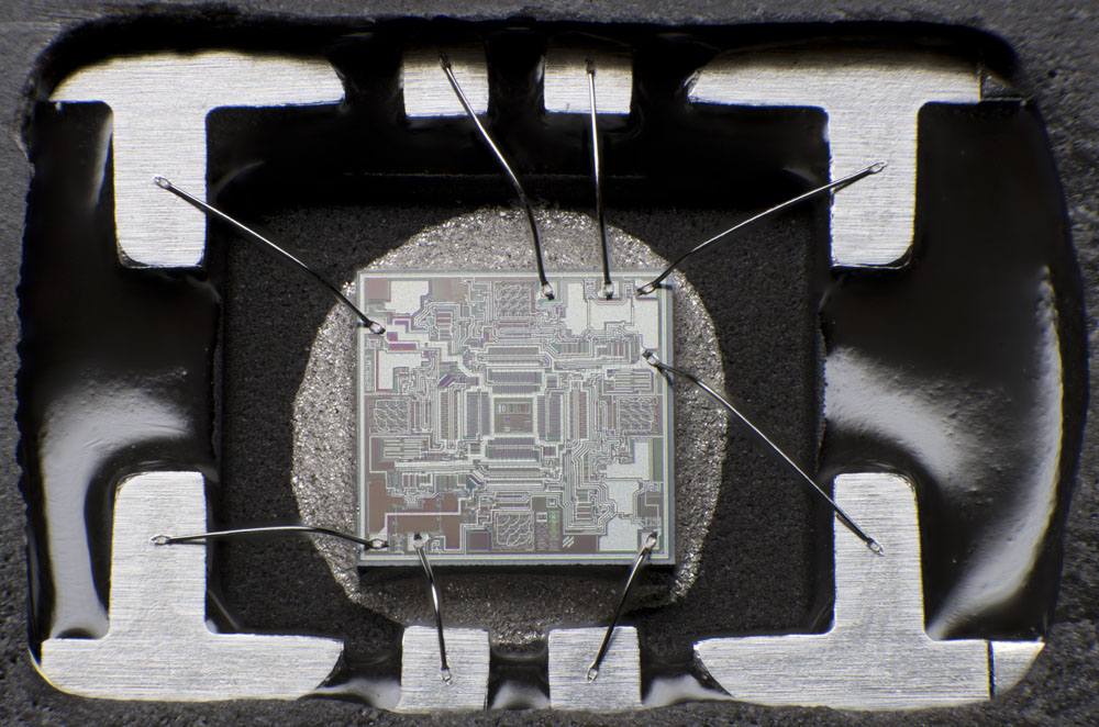
The edge length of the die is 1,9mm. The IEEE paper states that a 4µm process with two layers of poliysilicon is used, which was actually optimized for digital CMOS circuits. This can be very useful if you want to combine this opamp with digital circuits.
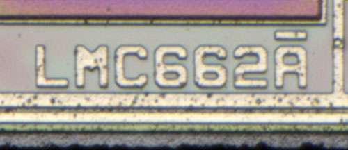
As will become clear later, the quad opamp LMC660 and the dual opamp LMC662 basically share the same die. They differ just in the metal layer. This metal layer here shows the designation LMC662. The letter A could stand for a first revision.
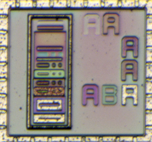
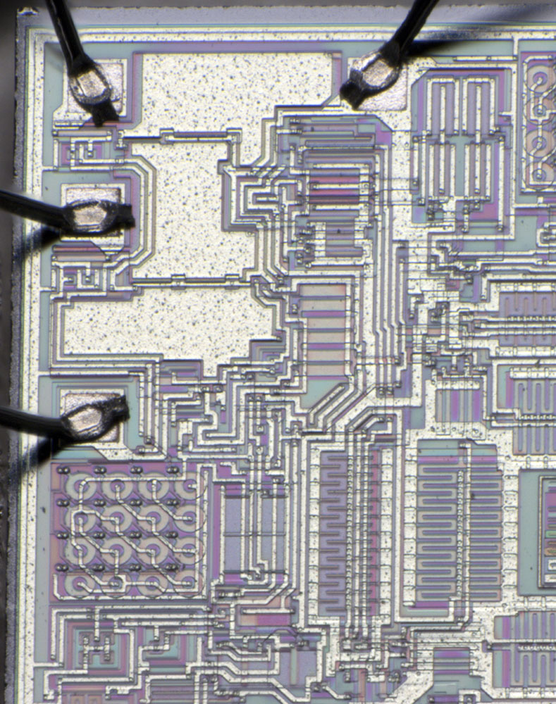
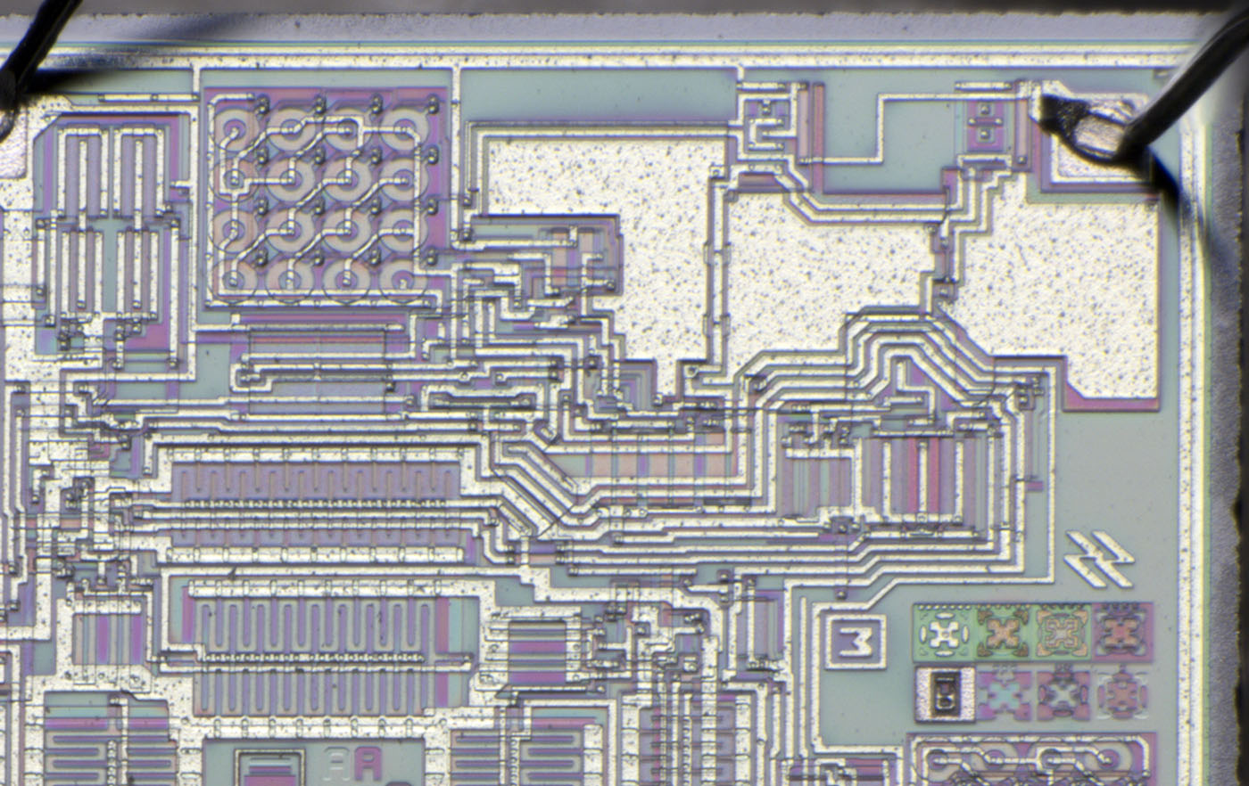
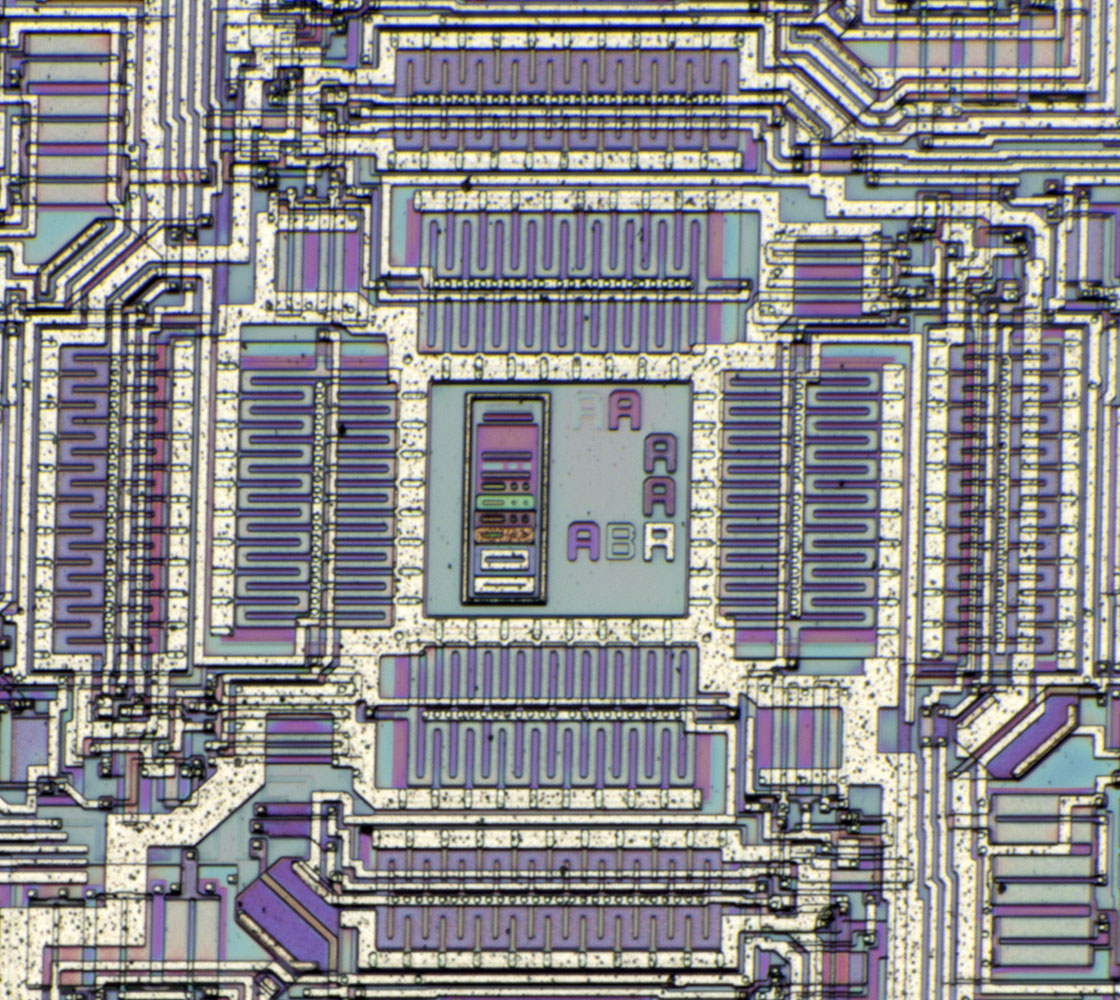
Seven mask revisions are shown in the center of the die. Accordingly, a mask has been revised once. The structures next to the mask revisions allow an evaluation of the imaging quality.
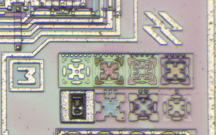
On the right edge, seven complex structures are shown under the National Semiconductor logo. Dots number the structures. Here, in addition to the imaging performance, the alignment of the masks against each other can be checked.
The magazine "Electronics Design Network" (11/2012) contains a picture of the LMC660 quadruple operational amplifier. According to the text, it is a representation that was used for troubleshooting. The different masks were printed with different colors on several foils. If one puts the foils on top of each other, overlapping layers create mixed colors and one can check the structures quite efficiently.
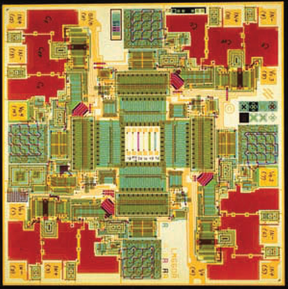
The already referenced IEEE paper contains a picture of the structures of the LMC660. Thick black lines show the areas of the four operational amplifiers. In the left area, the bias circuit is marked.
The input transistors M1/M2 (green) and the transistors of the associated current mirror M3/M4 (yellow) are each located in places where they are disturbed as little as possible. On the one hand, thermal gradients are problematic, which result primarily from the power dissipation of the output stage transistors (red). The alignment of output stages and input transistors on the symmetry axes ensures that thermal gradients have a very similar effect on both paths of the differential amplifier and thus compensate each other. Another issue is mechanical stress that result from integration into the package. These loads are also lowest on the symmetry axes.
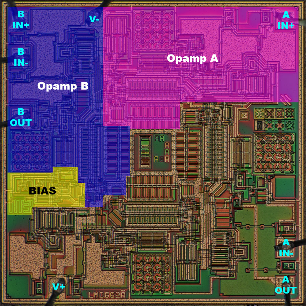
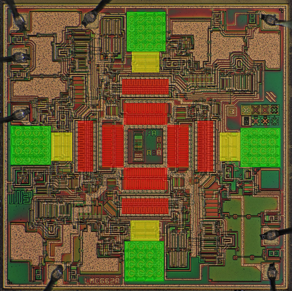
Apart from the metal layer, the dual opamp LMC662 uses the same design as the quadruple opamp LM660. The two opamps on the right and bottom edge remain unused here.
The individual components of the opamp can still be recognized quite well despite the two layers of polysilicon. Particularly noticeable are the three large capacitors next to the input and the output stage transistors.
The inputs of the opamps are equipped with protection circuits. According to the IEEE article, there is a 20Ω current-limiting resistor, followed by protective diodes to the supply potentials. The presence of these diodes is noteworthy because their leakage current must be low enough not to raise the very small input current of the opamp too much. In this context, it is surprising that the IEEE paper specifies a summed leakage current of 50fA, while the bias current should typically be just 2fA.

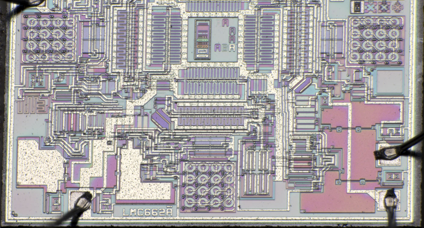
Under the metal layer there are four complete opamps. The metal layer above the unused opamps has been heavily modified. The main reason seems to be the different pinning in the smaller package. In order to connect the pins to the circuit in a meaningful way, the bondpads had to be moved.
The input transistors M1/M2 consist of eight circular elements each, which are interleaved in such a way that thermal gradients affect both paths of the differential amplifier as equally as possible. A similarly strong interleaving is implemented in the OPA627 (
https://www.richis-lab.de/Opamp22.htm). The transistors M3/M4, which represent the current mirror of the differential amplifier, are each divided into at least two transistors and cross-connected.
The source contacting (red) is inconspicuous. However, the IEEE paper describes that the different distances to the individual transistors are quite critical and can lead to an unbalanced behavior of the differential amplifier. Accordingly, 50 different configurations were simulated until the structure seen here was deemed optimal.
The highside and lowside transistors are quite large so that they can handle the high output currents.
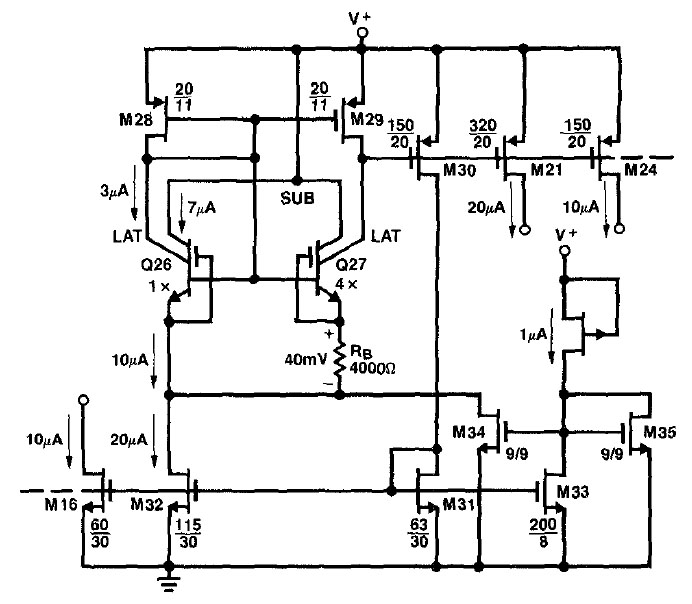
In a CMOS circuit, generating a stable reference voltage is a challenge. In the LMC662, one uses a bandgap reference based on the two special NPN transistors Q26/Q27. These are partially lateral bipolar transistors that can be implemented within a CMOS process.
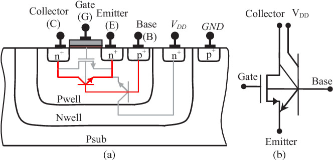
The structure of such a lateral bipolar transistor can be seen in the IEEE publication "Photodetection With Gate-Controlled Lateral BJTs From Standard CMOS Technology". An n-channel MOSFET inherently contains a parasitic NPN transistor, which has been subsequently colored red here. To use this transistor, the gate of the MOSFET must be connected in such a way that this area is always blocked.
The construction contains a second, parasitic collector. This must be connected to the positive supply potential so that the transistor remains isolated from the substrate. At the same time, however, this means that a current flows through this collector that is proportional to the current through the lateral collector. In order for the lateral collector to take a relevant share of the current, it must be placed as close as possible to the emitter. The current distribution is strongly influenced by production variations and cannot be controlled excessively well. The circuit of the bandgap reference ensures that this tolerance does not have an excessive influence on the reference voltage.
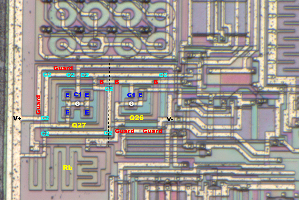
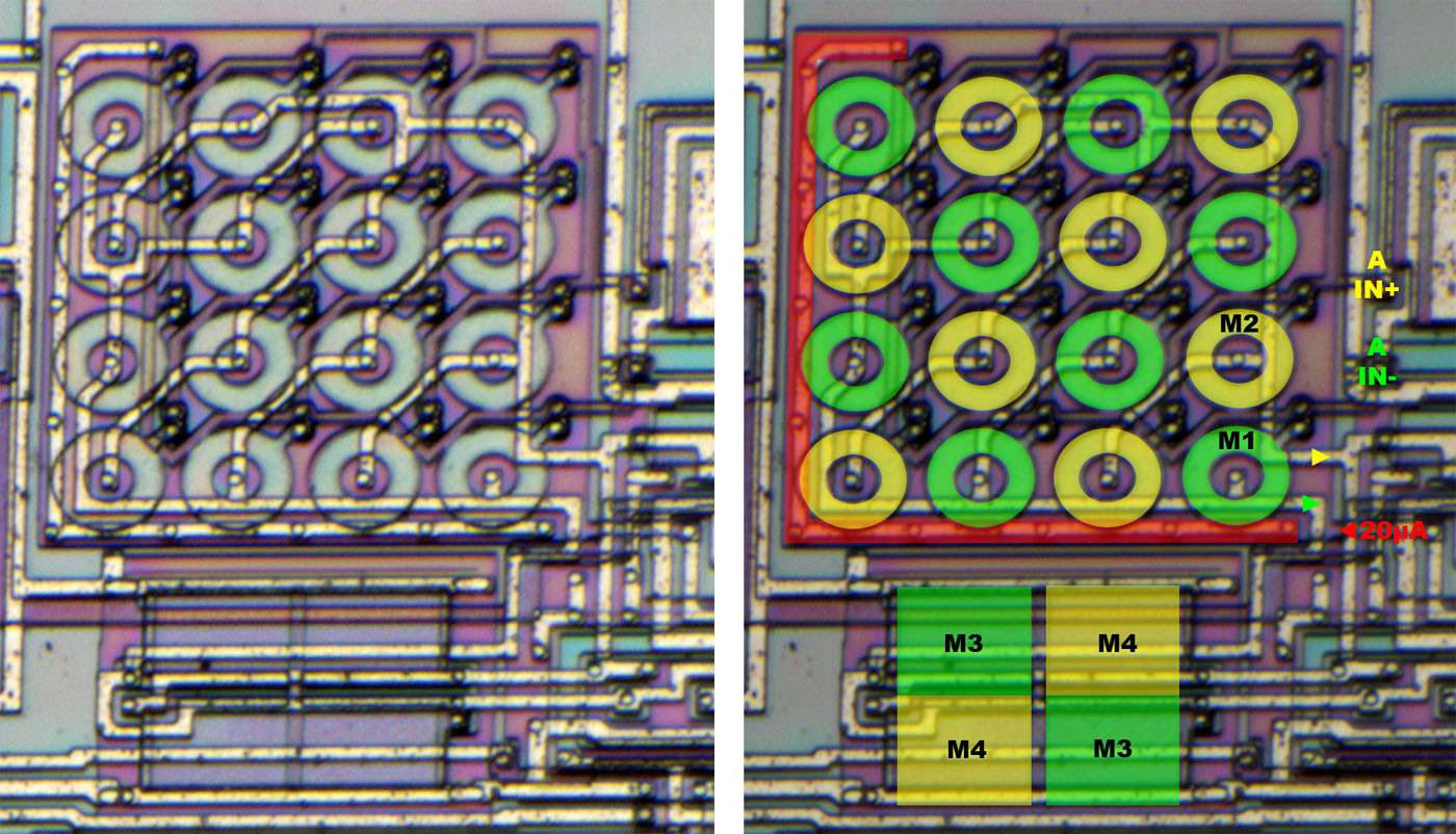
Viewed from above, such CMOS NPN transistors have a concentric structure. As usual for a bandgap reference, the two transistors Q27/Q26 have emitter areas of different sizes. In the LMC662, the ratio of the areas is 4:1.
Emitter and gate are connected to each other. Here in the picture, the difference is hardly visible due to the small structures. The purple appearing area is the gate electrode, within which the individual emitters are located. Directly around the gate electrode the lateral collector C1 is tapped. The frame around this construct is the base area, which in turn is surrounded by the collector C2. While C2 contacts the positive supply, the substrate is connected to the negative supply through the outermost frame.
https://www.richis-lab.de/Opamp62.htm 


