Author Topic: Transistors - die pictures  (Read 191202 times)

0 Members and 1 Guest are viewing this topic.

Offline NoopyTopic starter

  • Super Contributor
  • ***
  • Posts: 1734
  • Country: de
    • Richis-Lab
Re: Transistors - die pictures
« Reply #800 on: March 22, 2024, 05:08:28 am »
One addition to the whole topic:

This is a IRLZ44N!
The N version has a little lower Vds (55V vs. 60V), a little lower resistance and allows a little less current flow (47A vs. 50A).
Well it´s obviously the next generation, not the same...

Offline MarkT

  • Frequent Contributor
  • **
  • Posts: 367
  • Country: gb
Re: Transistors - die pictures
« Reply #801 on: March 23, 2024, 10:22:30 am »
Noopy, I see you opened up an RF power transistor above - the ceramic is likely BeO which is highly toxic if disrupted - its not a good idea to mess with these devices - you expressed amazement that the "ceramic" could handle the 195W rating - this strongly suggests it _is_ BeO which has very high thermal conductivity (can be better than aluminium, not quite as good as copper).  BeO is also a very high quality dielectric at RF, which is why it is chosen for RF devices despite the hazards.

If you aren't already taking precautions to avoid exposure to BeO fragments or dust, please do so, your health is more important than a few die pictures...
 

Offline NoopyTopic starter

  • Super Contributor
  • ***
  • Posts: 1734
  • Country: de
    • Richis-Lab
Re: Transistors - die pictures
« Reply #802 on: March 23, 2024, 10:53:53 am »
Thank you for your advice MarkT.
I have opened a lot of BeO devices. I know that BeO is problematic. In my view it´s ok to open such parts as long as you don´t break or grind the ceramic. I´m very cautious while opening such devices and I usually do it outside with a mask on.

 :-+

Offline NoopyTopic starter

  • Super Contributor
  • ***
  • Posts: 1734
  • Country: de
    • Richis-Lab
Re: Transistors - die pictures
« Reply #803 on: March 30, 2024, 04:26:30 am »


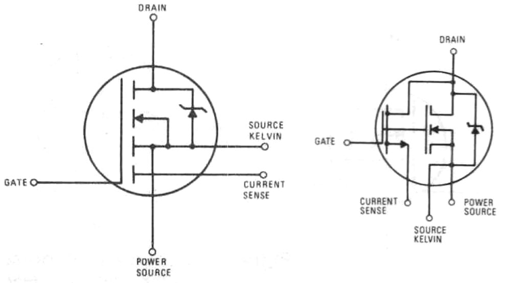
The IRC540 belongs to a group of special MOSFETs that International Rectifier had in its programme under the name HEXSense. The circuit diagrams above are taken from International Rectifier Application Note 959B. HEXSense MOSFETs offer a special path that facilitates current measurement. The symbol on the left is common. However, the mode of operation is less clear there. The right-hand symbol is easier to understand. You can see that there are two MOSFETs connected in parallel. The symbol of the left-hand MOSFET is somewhat misleading. It has exactly the same structures as the right-hand MOSFET and is even located within its structures. However, the left-hand MOSFET is significantly smaller and therefore only conducts a small proportion of the total current via the Current Sense pin. The small current is much easier to measure than the large load current. The ratio of the areas defines the ratio of the current distribution, which allows the total current to be determined.

The second additional pin represents a Kelvin connection of the source potential. With power transistors, such a contact is usually used to realise the most ideal control possible. Increasing load currents generate voltage drops at the inductances of the bondwires and the pins of the package. These voltage drops initially reduce the effective gate-source voltage directly at the silicon, which reduces the switching speed. If the Kelvin contact is used for gate control, this is independent of the load current. With HEXSense MOSFETs, the Kelvin contact can also be used for more effective gate control. However, it is also required to realise the most accurate current measurement. The smaller MOSFET should work with the same current paths and resistances as the MOSFET that carries the majority of the load current.


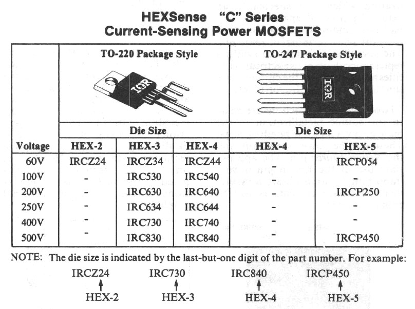
The HEXSense MOSFETs were based on the third generation HEXFET process, which was introduced in 1986 according to the International Rectifier Application Note 959B. This application note lists the different variants of HEXSense MOSFETs. The penultimate number of the designation shows which die size was used. The sizes HEX-2 to HEX-5 were used for the HEXSense MOSFETs. The smaller HEX-1 and HEX-Z variants were also used for the simple MOSFETs.

The IRC540 therefore uses size HEX-4 and has a reverse voltage of 100V. At room temperature, the IRC540 can conduct a drain current of 28A continuously. A short-term current of 110A is permissible. The ratio between load current and sense current is typically 2680:1, with a tolerance of approximately +/-4%. In addition, there is a temperature drift of approximately +/-1%. The typical Rdson is 77mΩ. The package allows a power dissipation of up to 150W.


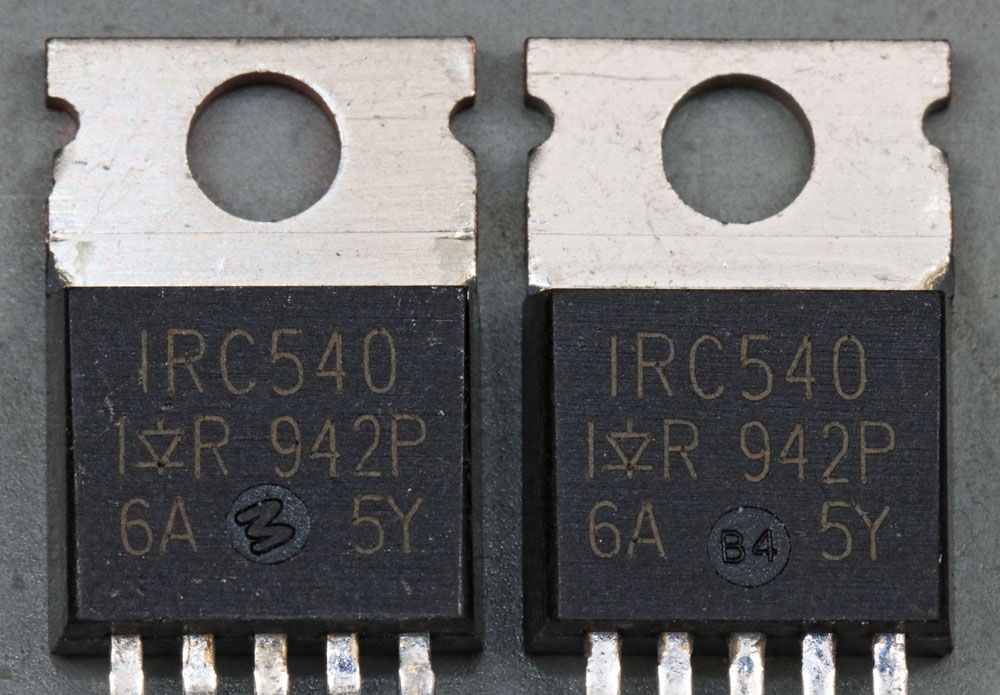
The two IRC540 shown here are from Pollin. They were originally three. The visual appearance let us doubt that they are original parts. The marking says exactly the same. However, the lettering on the right is slightly shifted to the left. The embossed characters are even more striking. Despite the same labelling, a twisted M is depicted on the left, while on the right there are the characters B4.


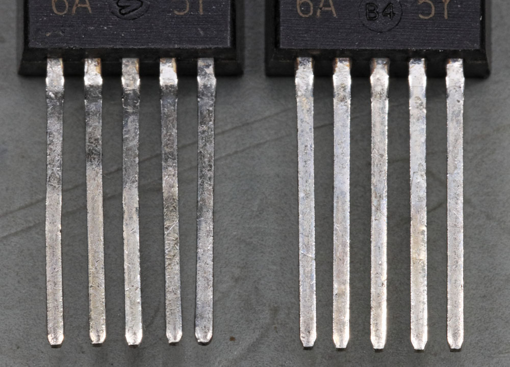
On closer inspection, the pins of the MOSFETs are noticeably bent. However, they still appear to be the original pins. In case of used components, new pins are sometimes fitted directly under the package.


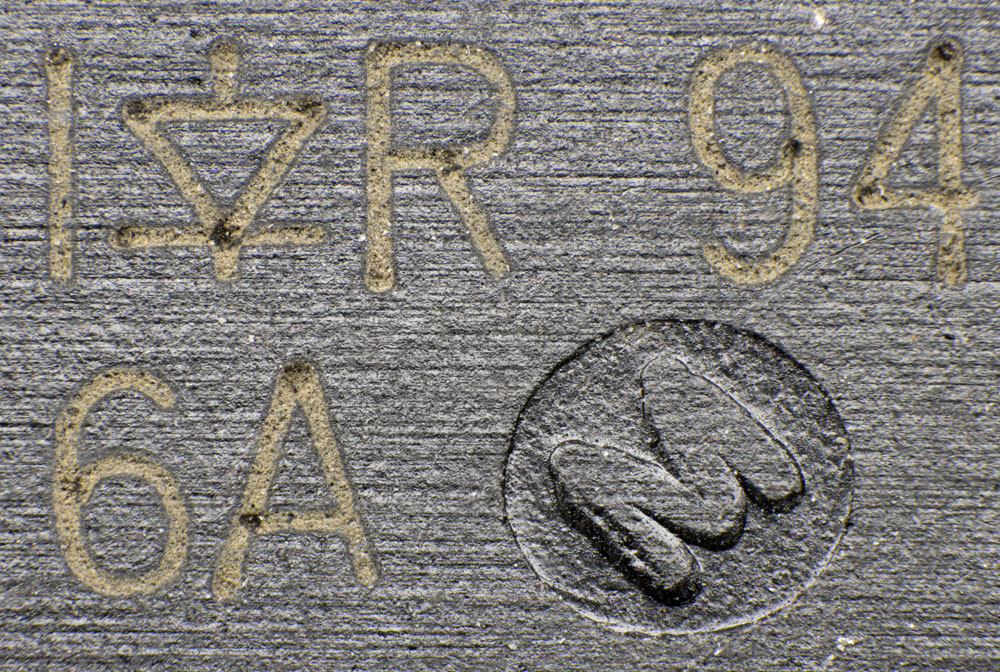
Knowing that it is a fake, you can recognise the grooves on the surface that were created when the case was sanded down. However, they are not overly noticeable. The indentation with the letter M, on the other hand, is more conspicuous. The indentation is shallower in the upper area than in the lower area. Here you can also recognise the original structure of the surface.


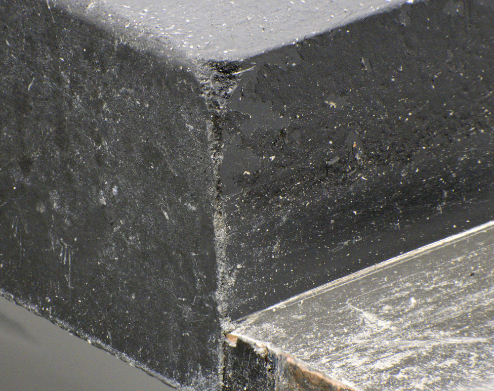
Looking from the side, it becomes even clearer that these are fakes. Apart from the fact that one corner of the case is broken off, you can see the layer of lacquer that was applied to the sanded package.


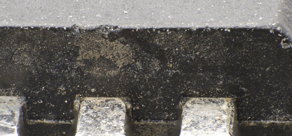
The underside of the package is noticeably dirty.


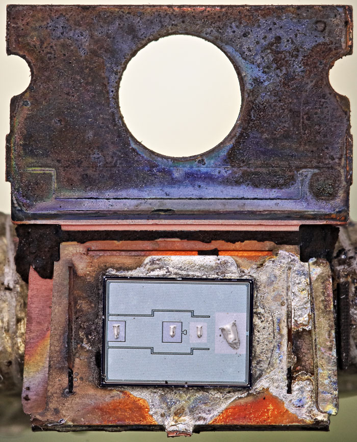
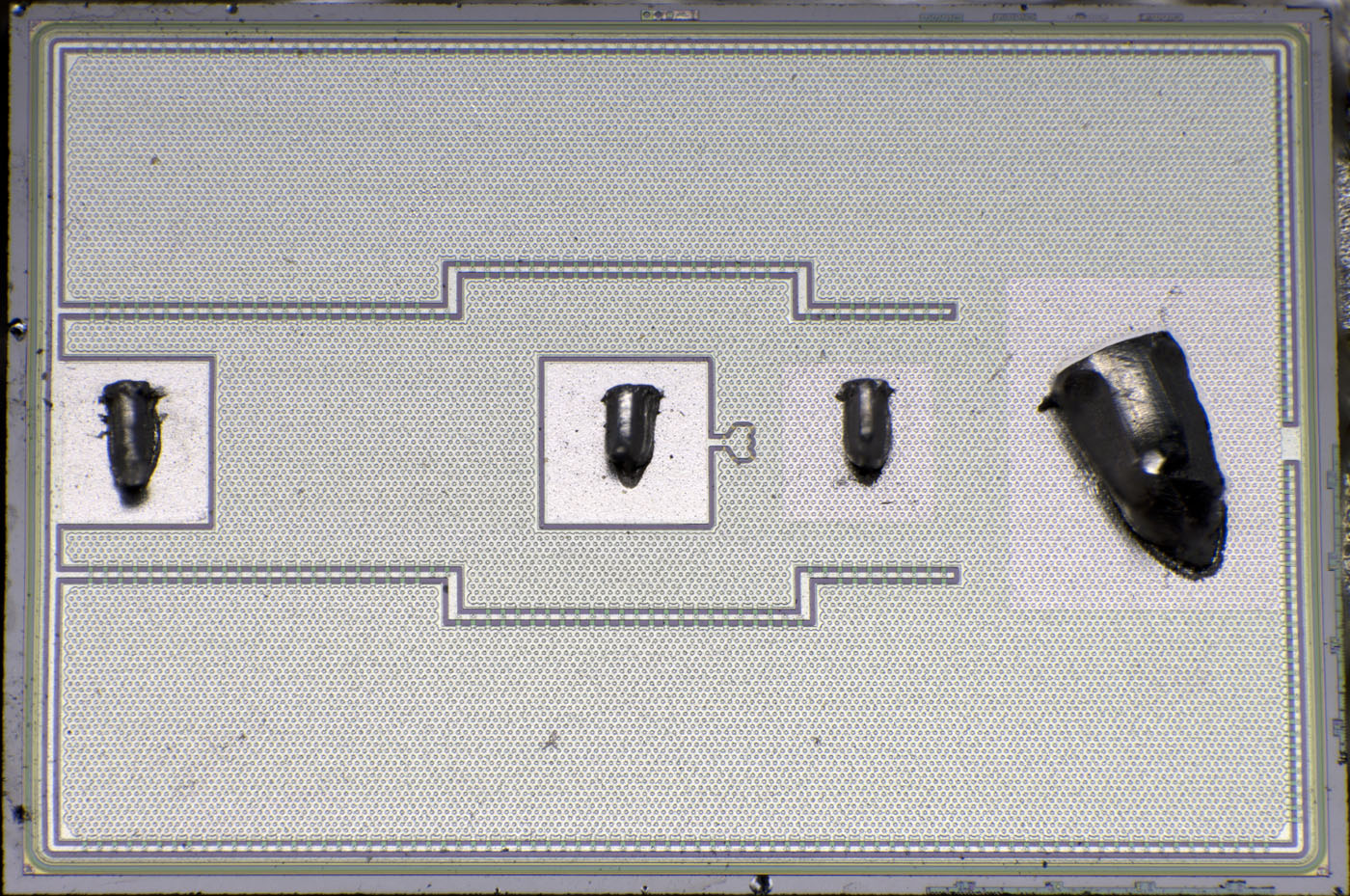
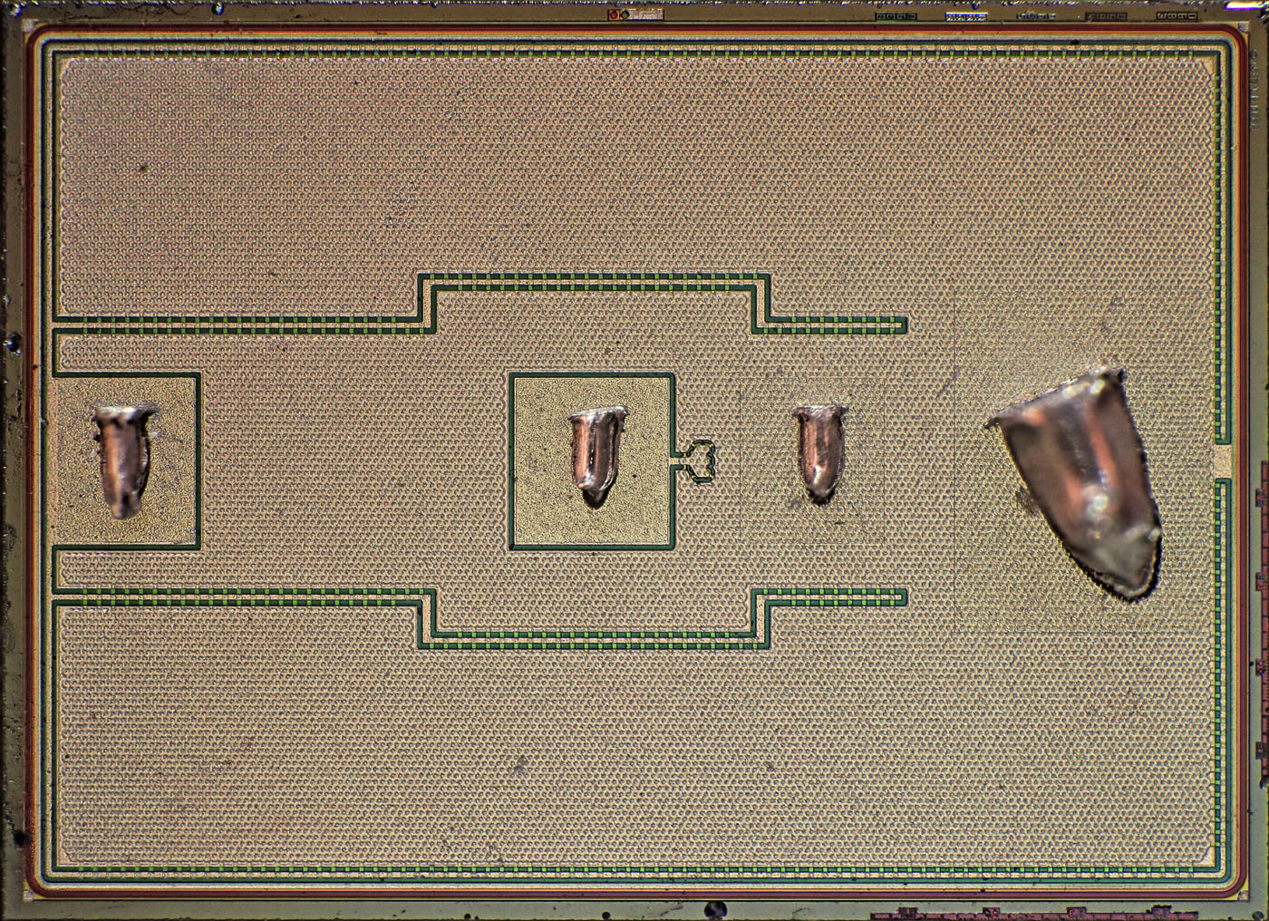
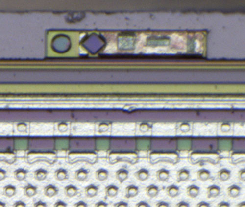
The package contains a die with an edge length of 4,6mm x 3,3mm.


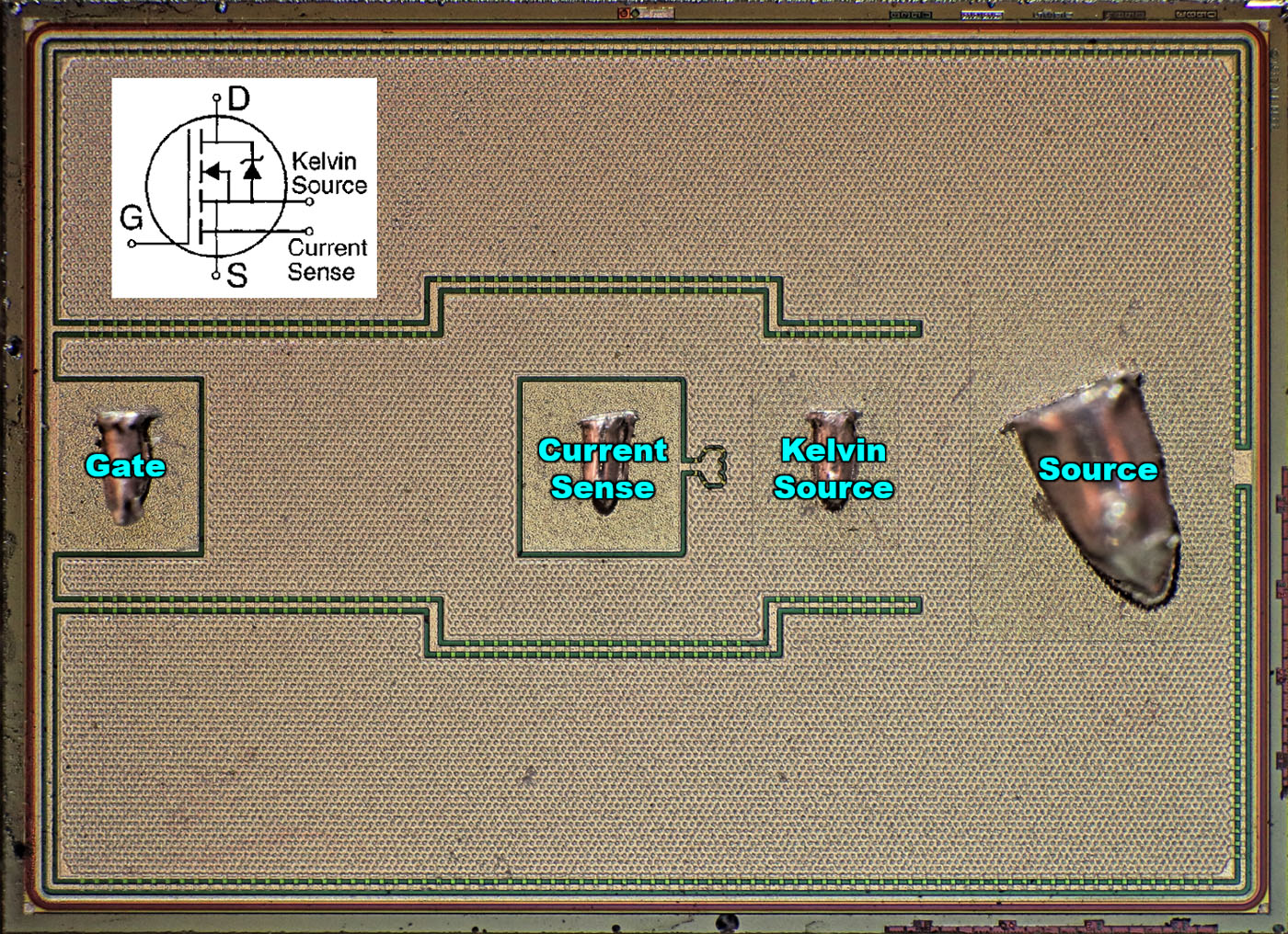
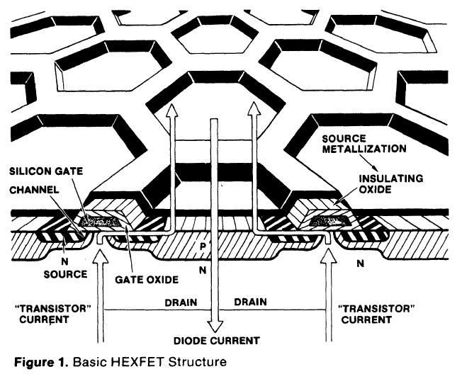
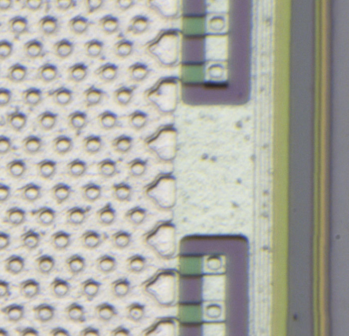
As usual with a MOSFET, the large metal surface represents the source potential. The gate potential is contacted on the left and gets distributed into the surface of the transistor via a surrounding frame and two stubs. The source contact for current measurement is located in the centre of the die. To the right, the Kelvin contact allows an unloaded contacting of the source potential. The International Rectifier Application Note 959B emphasises that it is important for good current measurement that the Kelvin contact is placed close to the bondpad for current measurement.


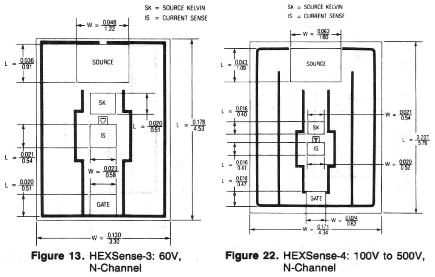
Here it becomes clear that these are counterfeit parts. The International Rectifier Application Note 964D shows how the different HEXFET generations are constructed. Both the dimensions and the structures correspond to those of a HEXSense-3 MOSFET with a reverse voltage of 60V. It was therefore originally an IRCZ34. The IRC540, a HEXSense-4 MOSFET with a dielectric strength of 100V, would have a significantly different structure and the die would be 1mm longer in both width and length.

The IRCZ34 shows typically a slightly lower impedance than the IRC540 (50mΩ / 77mΩ) and allows a slightly higher current flow (30A / 28A). However, with 60V the dielectric strength of the IRCZ34 is significantly lower than the 100V of the IRC540. In an application designed for the IRC540, the forgery would fail quickly.


The typical hexagonal structures of HEXFETs were already recognisable in the overview. The International Rectifier HEXFET Databook shows how the structures are organised in detail.


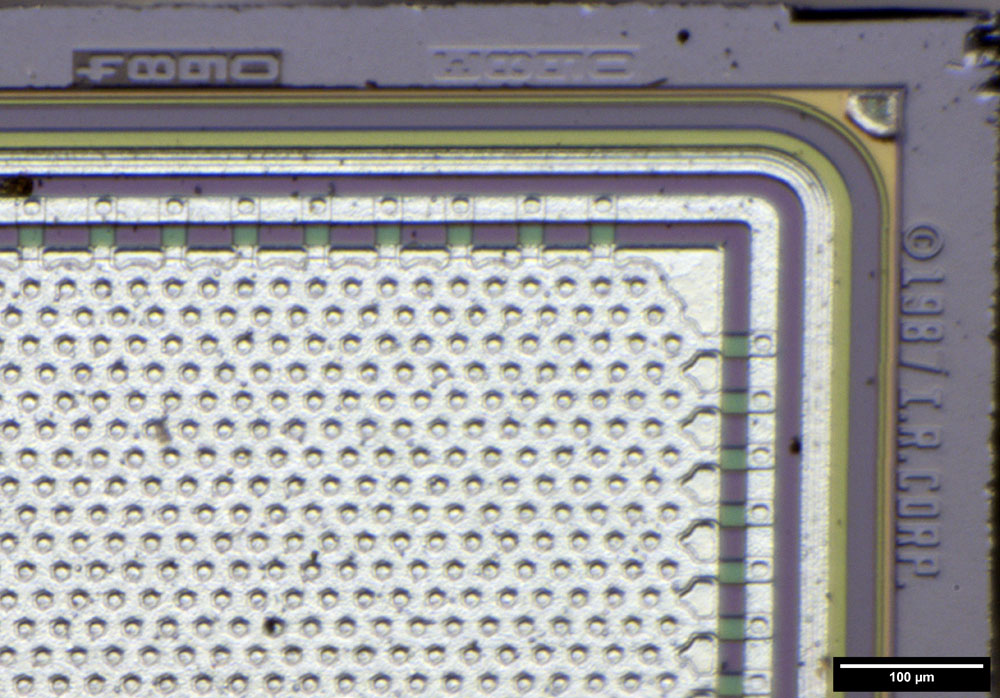
As is usual with MOSFETs from International Rectifier, some masks are shown on the upper edge. On the right is the copyright and a reference to the year 1987.

The contacts of the individual MOSFETs can be seen through the metal layer. The distance from centre to centre is approximately 24µm. The gate potential, which surrounds the contacts and thus controls the current flow, is fed in at the side.


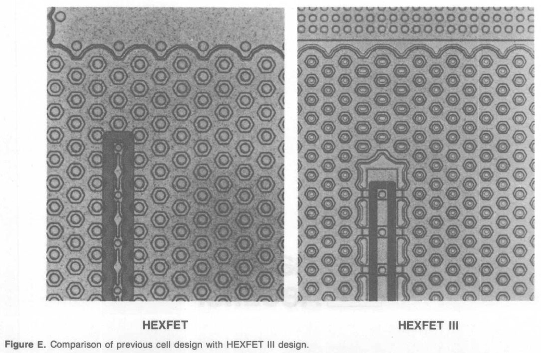
The International Rectifier Application Note 966A contains a detailed picture of the structures of the third HEXFET generation. Compared to the previous design, the structures have become slightly smaller.


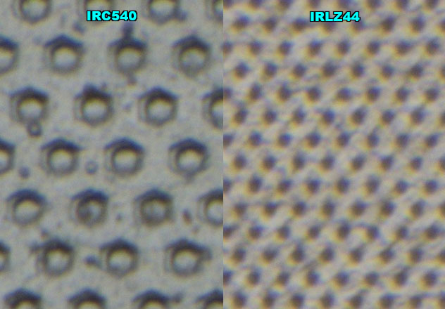
The structures in the IRLZ44N are even smaller (https://www.richis-lab.de/FET38.htm). It is probably based on the fifth generation of the HEXFETs.


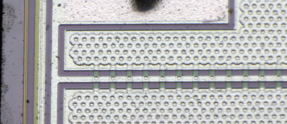
It is noticeable that the gate potential is not simply conducted into the active area with the lowest possible impedance. In contrast to the right edge, at the left edge there are no connections at all to the metal layer with the gate potential. Where the gate line describes a step, the gate potential has also only been connected to the active area at selected points. The steps were apparently created due to the current sense bondpad, under which there are no active structures.


The source potential is connected to the frame at the right edge. There is probably some potential control there in order to optimise the electric field distribution.


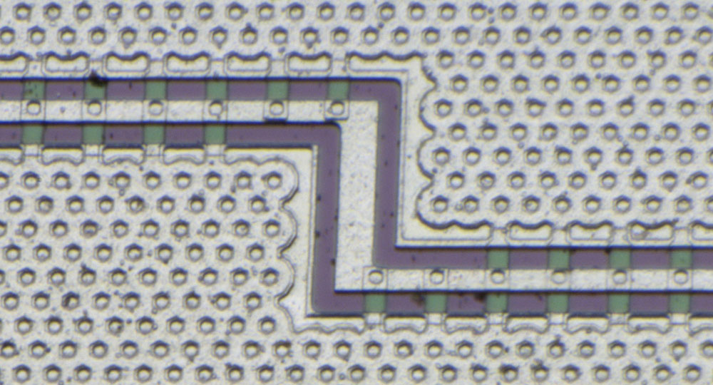
The source contact for current measurement contacts only 12 cells. Here, too, you can see that the gate electrodes have been carefully contacted. The gate area has been broken up and only partial contacts have been integrated between the two areas.

The datasheet describes a current ratio of 1:1.410 for the two transistors of the IRCZ34, whereby the manufacturing tolerance alone is already +/-70. Added to this are the fluctuations in drain current, temperature and gate-source voltage. If we calculate with the ratio 1:1.410 and assume that the current distribution corresponds exactly to the distribution of the individual transistors, the load transistor should be constructed with 16.920 transistors. In fact, there are 18.145 transistors, which is slightly more than you would expect. The current is probably not distributed ideally and the slightly different ratio compensates for this.


A test structure is shown at the top edge, which allows the alignment of the masks to be checked against each other.


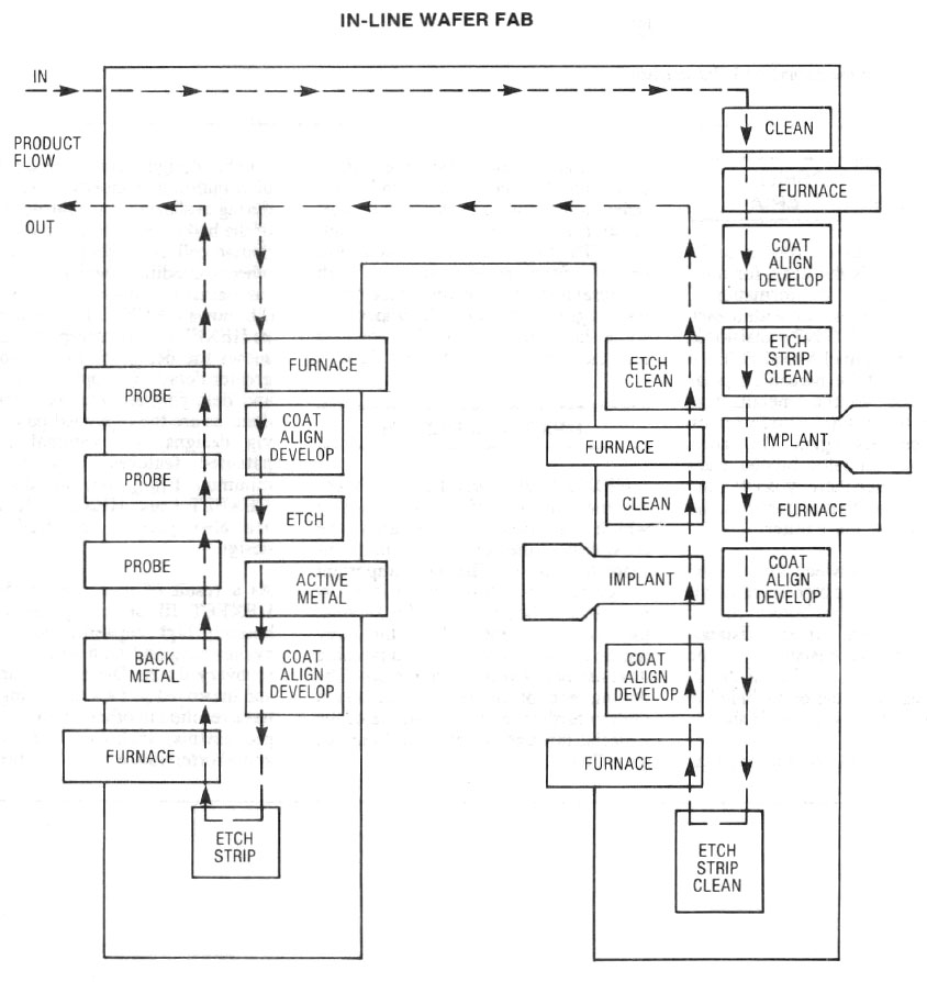
The International Rectifier Application Note 966A contains a simple illustration that provides an overview of how the HEXFET transistors were manufactured. In order to minimise production times, a production line has been set up that the MOSFETs can pass through in a linear fashion, which is otherwise rather unusual in the semiconductor industry.


https://www.richis-lab.de/FET39.htm

 :-/O
 
The following users thanked this post: Gyro, RoGeorge, ch_scr, iMo, D Straney

Offline Gyro

  • Super Contributor
  • ***
  • Posts: 9507
  • Country: gb
Re: Transistors - die pictures
« Reply #804 on: March 30, 2024, 10:23:04 am »
Even after seeing many examples, it still amazes me that it is possible to bond the heavy source lead without destroying the fine underlying structure.
Best Regards, Chris
 

Offline NoopyTopic starter

  • Super Contributor
  • ***
  • Posts: 1734
  • Country: de
    • Richis-Lab
Re: Transistors - die pictures
« Reply #805 on: March 30, 2024, 04:32:38 pm »
Even after seeing many examples, it still amazes me that it is possible to bond the heavy source lead without destroying the fine underlying structure.

Creating reliable bondwire connections is real magic.  :-+
And if you think of the speed and the yield they achieve today it´s just insane.

Offline NoopyTopic starter

  • Super Contributor
  • ***
  • Posts: 1734
  • Country: de
    • Richis-Lab
Re: Transistors - die pictures
« Reply #806 on: April 01, 2024, 04:59:25 pm »


The International Rectifier IRF530 is a HEXFET MOSFET with a dielectric strength of 100V. At room temperature the drain current may be 17A continuously. The specified peak current is 60A. The typical resistance is specified as 90mΩ. Up to 70W can be dissipated via the housing.


The package contains a die with an edge length of 3,0mm x 1,7mm. Apparently this is the same technology that was used in the IRF3708 (https://www.richis-lab.de/FET23.htm). The bigger structures distributing the gate and the source potential are designed in exactly the same way as in the IRF3708 and, as far as can be seen, the MOSFET structures themselves are also similar. The copyright with the year 2000 is fixed to the bottom edge. Three masks are shown on the upper edge. Five lines mark the center on all edges. All this can also be found on the die of the IRF3708.


https://www.richis-lab.de/FET40.htm

 :-/O
 
The following users thanked this post: RoGeorge

Offline David Hess

  • Super Contributor
  • ***
  • Posts: 16620
  • Country: us
  • DavidH
Re: Transistors - die pictures
« Reply #807 on: April 01, 2024, 08:57:17 pm »
I used so many IRF530s.  I still have a drawer filled with IRF9530s.  These are 88 watts.

We had so many problems sourcing parts at the time, that I had to use 125 watt IRF640s and IRF9640s instead, and I have a drawer full of those also.
 

Offline duak

  • Super Contributor
  • ***
  • Posts: 1041
  • Country: ca
Re: Transistors - die pictures
« Reply #808 on: April 02, 2024, 01:00:48 am »
I've got a couple of tubes of IRFP360s (400 V, 15 A) from 1991 or so.  Would these likely use a similar die?  Any thoughts on what the designers did to vary the geometry for higher breakdown voltage parts? 

I've been thinking of using them for the mother of all loads as I have a 100 x 20 x 8 cm heat sink extrusion and some 20 cm diameter fans. The higher on resistance of the older FETs should be helpful in spreading current throughout the die making them more useful for linear applications.
 

Offline David Hess

  • Super Contributor
  • ***
  • Posts: 16620
  • Country: us
  • DavidH
Re: Transistors - die pictures
« Reply #809 on: April 02, 2024, 01:26:34 am »
I've got a couple of tubes of IRFP360s (400 V, 15 A) from 1991 or so.  Would these likely use a similar die?  Any thoughts on what the designers did to vary the geometry for higher breakdown voltage parts?

I have a bag of TO-3 IRF531s (350 volts, 15 amps, 150 watts) from 1987.  I think all of the IRF parts from this era are Hexfets.

Going from page 2-5 of the Siliconix MOSPOWER Applications book which discusses it in detail, if the designers did everything correctly, breakdown is primarily limited by the diffusion concentration of the drain, which is also the PN junction making up the parasitic collector which forms the body diode.  Higher voltage parts require less doping, but this increases the resistivity which is proportional to the breakdown voltage raised to the 2.5 power.  So doubling the breakdown voltage increases the on-resistance by 5.7 times, explaining why high voltage power MOSFETs are so expensive.  Modern super-junction parts somehow get around this limitation.

Quote
I've been thinking of using them for the mother of all loads as I have a 100 x 20 x 8 cm heat sink extrusion and some 20 cm diameter fans. The higher on resistance of the older FETs should be helpful in spreading current throughout the die making them more useful for linear applications.

I do not think the higher channel resistance matters, so you do not get around the requirement for ballasting in parallel linear applications with high voltage parts.  What does matter is the temperature coefficient and where it reverses at higher drain voltage, but that depends on things other than size.
« Last Edit: April 02, 2024, 06:56:02 am by David Hess »
 

Offline NoopyTopic starter

  • Super Contributor
  • ***
  • Posts: 1734
  • Country: de
    • Richis-Lab
Re: Transistors - die pictures
« Reply #810 on: April 02, 2024, 02:30:06 am »
I've got a couple of tubes of IRFP360s (400 V, 15 A) from 1991 or so.  Would these likely use a similar die?  Any thoughts on what the designers did to vary the geometry for higher breakdown voltage parts? 

As David already said, for a higher breakdown voltage you need a thicker n- layer (https://en.wikipedia.org/wiki/Power_MOSFET#/media/File:Vdmos_cross_section_en.svg).
A thicker n- layer gives you more resistance, so either you agree with that or you make the die bigger. You can do both.

And beside this you can have a different generation (HEXFET Gen.1 / Gen.3 / Gen.5) adding another variable.


The higher on resistance of the older FETs should be helpful in spreading current throughout the die making them more useful for linear applications.

I´m not sure about that. In principle you are right (more resistance should give you a better current distribution). But the process adds some more variables. Perhaps there is a generation that has lower resistance but better linear behaviour because of a special trick in the production or in the geometry of the layers or whatever.
I would consult the datasheet / manufacturer. If it is a MOSFET for linear applications then it is good for linear applications...  ;)


I have a bag of TO-3 IRF531s (350 volts, 15 amps, 150 watts) from 1987.  I think all of the IRF parts from this era are Hexfets.

Yes, they are probably HEXFET generation 3.


Quote
I've been thinking of using them for the mother of all loads as I have a 100 x 20 x 8 cm heat sink extrusion and some 20 cm diameter fans. The higher on resistance of the older FETs should be helpful in spreading current throughout the die making them more useful for linear applications.

I do not think the higher channel resistance matters.  What does matter is the temperature coefficient and where it reverses at higher drain voltage, but that depends on things other than size.

Exactly!  :-+

Offline NoopyTopic starter

  • Super Contributor
  • ***
  • Posts: 1734
  • Country: de
    • Richis-Lab
Re: Transistors - die pictures
« Reply #811 on: April 12, 2024, 03:44:59 am »


More IRF!  ;D

The International Rectifier IRF1010NSPbF is another HEXFET MOSFET. As we know International Rectifier uses the N to identify components that have been updated, i.e. are based on a newer MOSFET generation. S stands for the D2PAK housing and PbF indicates that the component is lead-free.

The maximum blocking voltage is 55V. A continuous drain current of 85A is permissible at room temperature. A peak current of 290A is specified. The typical resistance is specified as 11mΩ. Up to 180W can be dissipated via the housing.


The housing of the IRF1010N contains a die with an edge length of 4,1mm x 3,0mm. Apparently, this is the same technology that was used in the IRF3708. The rough structures for the distribution of gate and source potential are designed in exactly the same way as in the IRF3708 and, as far as can be recognised, the MOSFET structures themselves are also identical. The copyright with the year 2000 is fixed to the bottom edge. Masks are shown on the upper edge. Five lines mark the centre on all edges. All this can also be found in the IRF3708 too.


https://www.richis-lab.de/FET41.htm

 :-/O
 
The following users thanked this post: exe, RoGeorge

Offline NoopyTopic starter

  • Super Contributor
  • ***
  • Posts: 1734
  • Country: de
    • Richis-Lab
Re: Transistors - die pictures
« Reply #812 on: April 17, 2024, 06:46:18 pm »


The International Rectifier IRF1404 shown here has the letter P in the second line, i.e. it is an IRF1404PbF (lead free). This version allows 202A, more than the original IRF1404 variant, which is only specified for a drain current of 162A. The IRF1404PbF allows up to 808A for short periods. The typical resistance for both variants is 4mΩ. The maximum reverse voltage is 40V. Up to 333W can be dissipated through the TO-220 package.


The marking is somewhat poor, but this seems to be common for the newer HEXFET MOSFETs in this package.


There are three holes in the surface of the package, which were obviously created when the mold compound was injected.


With its dimensions of 5,8mm x 4,2mm, the die is very large for a TO-220 package. In order to represent the low typical resistance, the source surface has been connected to the source pin with four thick bondwires.


The datasheet states that this is a seventh-generation HEXFET. Vertical stripes are visible on the surface of the source metallization, which result from the contacting of the individual MOSFET structures.


https://www.richis-lab.de/FET42.htm

 :-/O
 
The following users thanked this post: RoGeorge, iMo

Online RoGeorge

  • Super Contributor
  • ***
  • Posts: 6203
  • Country: ro
Re: Transistors - die pictures
« Reply #813 on: April 17, 2024, 07:59:13 pm »
When they give 4m\$\Omega\$ and 202A, that made me curious.  I've doubted that the outside terminals can withstand at 200A without melting, or at least going red hot, let alone the bonding wires.

The fine print in the datasheet https://www.infineon.com/dgdl/irf1404pbf.pdf?fileId=5546d462533600a4015355dae92618b0 says that the 202A continuous current would be supported, just that those 202A are a calculated value, based on the thermal resistance and the max allowed junction temperature.  The package limit is 75A, so the 202A continuous drain current is a lie.  Quote from the datasheet, remark 6 regarding max Id:
Quote
Calculated continuous current based on maximum allowable
junction temperature. Package limitation current is 75A.

The 4m\$\Omega\$ also seemed too small, and it has a fine print, too, remark 4 in the datasheet:
Quote
Pulse width ≤ 400μs; duty cycle ≤ 2%.
That is because the value is specified at Vgs = 10V and Id = 121A, which Id is higher than the max 75A continuous supported by the package, thus the time and the duty factor limitations.  OK, understandable.

But why is the Rds value specified at such high Id.  Why didn't they measure it at a 10 times lower or so current, and no pulses?  Is it something in the MOSFET physics, that makes it achieve very low Rds only at huge drain current, so they took the extra effort measuring pulses only to obtain a much lower Rds value for the datasheet (similar with the 202A continuous but no more than 75A)?

Why did they bother using huge current and pulses to measure Rds on?
« Last Edit: April 18, 2024, 04:07:52 am by RoGeorge »
 

Offline T3sl4co1l

  • Super Contributor
  • ***
  • Posts: 21688
  • Country: us
  • Expert, Analog Electronics, PCB Layout, EMC
    • Seven Transistor Labs
Re: Transistors - die pictures
« Reply #814 on: April 17, 2024, 08:22:48 pm »
You may find these thoughts of interest: https://electronics.stackexchange.com/questions/708541/how-can-tiny-mosfets-be-rated-for-relatively-high-current/708548#708548

Incidentally... what the hell happened to even generation HEXFETs?  1st is long since obsolete I guess (probably process doesn't exist anymore anyway), but I don't recall ever seeing "2nd generation" or etc., and they just jump to 3rd, 5th and 7th.  Or "advanced".

Tim
Seven Transistor Labs, LLC
Electronic design, from concept to prototype.
Bringing a project to life?  Send me a message!
 

Offline NoopyTopic starter

  • Super Contributor
  • ***
  • Posts: 1734
  • Country: de
    • Richis-Lab
Re: Transistors - die pictures
« Reply #815 on: April 17, 2024, 08:27:49 pm »
You are right. These currents are just for advertising.

I don´t know thy they did the resistance measurement at 121A...  :-//


Yes Tim, it seems like they just sold even numbers of their HEXFETs.

Offline Wolfgang

  • Super Contributor
  • ***
  • Posts: 1775
  • Country: de
  • Its great if it finally works !
    • Electronic Projects for Fun
Re: Transistors - die pictures
« Reply #816 on: April 18, 2024, 12:20:15 pm »
When they give 4m\$\Omega\$ and 202A, that made me curious.  I've doubted that the outside terminals can withstand at 200A without melting, or at least going red hot, let alone the bonding wires.

The fine print in the datasheet https://www.infineon.com/dgdl/irf1404pbf.pdf?fileId=5546d462533600a4015355dae92618b0 says that the 202A continuous current would be supported, just that those 202A are a calculated value, based on the thermal resistance and the max allowed junction temperature.  The package limit is 75A, so the 202A continuous drain current is a lie.  Quote from the datasheet, remark 6 regarding max Id:
Quote
Calculated continuous current based on maximum allowable
junction temperature. Package limitation current is 75A.

The 4m\$\Omega\$ also seemed too small, and it has a fine print, too, remark 4 in the datasheet:
Quote
Pulse width ≤ 400μs; duty cycle ≤ 2%.
That is because the value is specified at Vgs = 10V and Id = 121A, which Id is higher than the max 75A continuous supported by the package, thus the time and the duty factor limitations.  OK, understandable.

But why is the Rds value specified at such high Id.  Why didn't they measure it at a 10 times lower or so current, and no pulses?  Is it something in the MOSFET physics, that makes it achieve very low Rds only at huge drain current, so they took the extra effort measuring pulses only to obtain a much lower Rds value for the datasheet (similar with the 202A continuous but no more than 75A)?

Why did they bother using huge current and pulses to measure Rds on?

I think that the exaggerated claims of the marketing people are a potential threat to a brands credibility. If the claims have no relation to practical use why buy from these people ? I'd rather buy from somebody without a lot of disclaimers and smallprint in their datasheets.
 

Offline NoopyTopic starter

  • Super Contributor
  • ***
  • Posts: 1734
  • Country: de
    • Richis-Lab
Re: Transistors - die pictures
« Reply #817 on: April 18, 2024, 06:02:49 pm »
I think that the exaggerated claims of the marketing people are a potential threat to a brands credibility. If the claims have no relation to practical use why buy from these people ? I'd rather buy from somebody without a lot of disclaimers and smallprint in their datasheets.

I agree with you. I don´t like such marketing exorbitance either.  :-//

Offline NoopyTopic starter

  • Super Contributor
  • ***
  • Posts: 1734
  • Country: de
    • Richis-Lab
Re: Transistors - die pictures
« Reply #818 on: April 19, 2024, 11:09:22 am »


The International Rectifier IRF2804 shown here has the letter P in the second line. It is therefore the lead-free version IRF2804PbF. In contrast to the IRF1404PbF, the lead-free version of the IRF2804 allows less drain current. The datasheet specifies a maximum possible continuous current of 250A for the MOSFET itself, whereby the housing limits the continuous current to 75A. The maximum permissible peak current is 1080A. The resistance is specified as 2mΩ. The blocking voltage is 40V. Up to 300W can be dissipated via the TO-220 housing.


With 5,8mm x 4,3mm the die is slightly larger than the die of the IRF1404PbF. Here too, the source area is connected to the source pin with four thick bondwires. The frame structures are relatively similar, but not quite the same.


In detail it becomes even clearer that this is a different design to the IRF1404PbF. The metallization shows none of the underlying structures. Either the individual transistor elements are too small to be resolved or the source metallization is significantly thicker and thus conceals any unevenness.


Some masks appear to be depicted on the lower edge.


https://www.richis-lab.de/FET43.htm

 :-/O
« Last Edit: April 19, 2024, 03:45:53 pm by Noopy »
 
The following users thanked this post: RoGeorge, ch_scr


Share me

Digg  Facebook  SlashDot  Delicious  Technorati  Twitter  Google  Yahoo
Smf