Author Topic: Voltage regulators - die pictures  (Read 30446 times)

0 Members and 1 Guest are viewing this topic.

Offline NoopyTopic starter

  • Super Contributor
  • ***
  • Posts: 1735
  • Country: de
    • Richis-Lab
Voltage regulators - die pictures
« on: June 08, 2020, 04:44:11 am »
Are you interested in more die pictures?
I have taken some pictures of a LM317 and soon will upload a high-current voltage regulator.
If you want me to post such pictures here to cheer you and discuss them give me a thumps up.  ;)

And now the LM317:


It´s a 1991 National Semiconductor part in a TO39 package.


Here you can see the bandgap reference (transistor ratio 1:10). A modification of the metal layer can change the ratio to 2:10.


They use two metal fuses and one zener fuse for adjusting the reference voltage.
Metal fuses are nc, zener fuses are no. I assume that they tried to get a midposition after production so they don´t have to open too much metal fuses. Opening metal fuses leads to contamination of the test needles.


I assume the circuit on the left side modifies the bias of the Regulator curcuits depending on the voltage over the LM317. Can somebody confirm that?  :-/O


Some more pictures on my website:

https://www.richis-lab.de/LM317_01.htm

 :popcorn:

Offline magic

  • Super Contributor
  • ***
  • Posts: 6779
  • Country: pl
Re: Voltage regulators - die pictures
« Reply #1 on: June 08, 2020, 07:27:54 am »
On the schematic, Q2~Q5 looks like the "constant gm bias" circuit. I suppose Q3 has more emitter area than Q5 while Q2 and Q4 and their emitter resistors are identical. It's a trick to generate currents through Q3 and Q5 such that transconductance of those two and other similar transistors maintains some defined value regardless of die temperature.

Q1 and R6 provide a small current which starts the bias generator. Otherwise neither the NPNs nor the PNPs would turn on by themselves because their bases are driven by each other. D1 seems to limit this current when Vin-Vout is high.

edit
Somewhere, there has to be thermal shutdown too.
« Last Edit: June 08, 2020, 07:31:55 am by magic »
 
The following users thanked this post: Noopy

Offline NoopyTopic starter

  • Super Contributor
  • ***
  • Posts: 1735
  • Country: de
    • Richis-Lab
Re: Voltage regulators - die pictures
« Reply #2 on: June 08, 2020, 10:11:37 am »
On the schematic, Q2~Q5 looks like the "constant gm bias" circuit. I suppose Q3 has more emitter area than Q5 while Q2 and Q4 and their emitter resistors are identical. It's a trick to generate currents through Q3 and Q5 such that transconductance of those two and other similar transistors maintains some defined value regardless of die temperature.

Q1 and R6 provide a small current which starts the bias generator. Otherwise neither the NPNs nor the PNPs would turn on by themselves because their bases are driven by each other. D1 seems to limit this current when Vin-Vout is high.

edit
Somewhere, there has to be thermal shutdown too.

Thank you very much, magic.  :-+

I have nothing more to add.  :)

Offline NoopyTopic starter

  • Super Contributor
  • ***
  • Posts: 1735
  • Country: de
    • Richis-Lab
Re: Voltage regulators - die pictures
« Reply #3 on: June 08, 2020, 10:18:21 am »
But wait, one more sentence!

With your explanation an some closer examination of the red part it seems to me the red part has to do the thermal shutdown. It can shut down the linear regulator and Q6, Q7, Q9 are somewhat crazy wired. That part has to be the thermal shutdown. Although I have to think about the operation principle.

Offline magic

  • Super Contributor
  • ***
  • Posts: 6779
  • Country: pl
Re: Voltage regulators - die pictures
« Reply #4 on: June 08, 2020, 02:48:47 pm »
Well, Q6 is just an emitter follower. If Q7 Vbe decreases 2mV/°C due to temperature, R10 voltage increases equally and R8 voltage increases 6mV/°C. Q9 Vbe also decreases 2mV/°C so we have 8mV/°C equivalent increase of Q9 base drive. This goes to Q11 and turns it on.

All of that assumes that Q7 base is held at constant voltage which is probably not exactly true, but I suppose similar principles apply. If this circuit isn't doing thermal limiting then I have no idea what else it could do.

I'm also ignoring that the increased Q9 current reduces Q6 current, this is hopefully insignificant.

Corollary: there is no real shutdown with hysteresis, it just throttles the output so as to maintain roughly constant die temperature.
 

Offline David Hess

  • Super Contributor
  • ***
  • Posts: 16621
  • Country: us
  • DavidH
Re: Voltage regulators - die pictures
« Reply #5 on: June 08, 2020, 04:59:56 pm »
Without the startup circuit, the IC may still start if the supply voltage is applied rapidly through capacitive coupling.  But it is embarrassing to release an IC which does not start if the supply voltage is applied slowly.

Didn't Bob Pease mention that they had a Czar of startup circuits at one point?
 

Offline floobydust

  • Super Contributor
  • ***
  • Posts: 7007
  • Country: ca
Re: Voltage regulators - die pictures
« Reply #6 on: June 08, 2020, 07:01:44 pm »
I would say the SOA protection is Czar level.
NS 1975 Voltage Regulator Handbook (before LM317) mentioned IC thermal shutdown typically is done with a transistor biased at ~0.4V VBE located near the pass-transistor on the die. It turns on when hot. But nothing so simple here. I keep looking for the error amplifier as a diff amp like other NS Vregs.
1978 schematic has no 50R resistor or 6V zener at the ADJ pin.
 

Offline magic

  • Super Contributor
  • ***
  • Posts: 6779
  • Country: pl
Re: Voltage regulators - die pictures
« Reply #7 on: June 08, 2020, 08:09:10 pm »
My recent ST datasheet doesn't have it either, but by the looks of it I'm not sure if the schematic has ever been updated since the '70s ;)

Maybe the Zener thing is a red herring and they simply wanted a diode protecting the bandgap cell from reverse breakdown in the event of ESD or reference capacitor discharge. C-B shorted NPNs just happen to have low breakdown voltage when used as diodes.

Q22 and that anonymous NPN near it (Q23?) are a weird thing, looks like some positive feedback pumping current into Q23 base when Q23 conducts. Is it trying to cancel Q25 base current and increase output stage input impedance or something more? :-//
« Last Edit: June 08, 2020, 08:10:41 pm by magic »
 

Offline NoopyTopic starter

  • Super Contributor
  • ***
  • Posts: 1735
  • Country: de
    • Richis-Lab
Re: Voltage regulators - die pictures
« Reply #8 on: June 08, 2020, 08:40:34 pm »
The 50Ohm resistor is contains fuses to adjust the reference voltage. Perhaps the first LM317 had worse specifications and did not need a trimming.

In my opinion the zener protects the bandgap reference from to much current. If ever the potential at the adjust pin goes a lot lower than on the Vout-Pin the small transistors will get killed. A 6V-zener limits the current to 0,5mA.

Yeah, Q22 and the no-name-transistor are somewhat strange...  :-//

Offline David Hess

  • Super Contributor
  • ***
  • Posts: 16621
  • Country: us
  • DavidH
Re: Voltage regulators - die pictures
« Reply #9 on: June 08, 2020, 11:44:48 pm »
I would say the SOA protection is Czar level.
NS 1975 Voltage Regulator Handbook (before LM317) mentioned IC thermal shutdown typically is done with a transistor biased at ~0.4V VBE located near the pass-transistor on the die. It turns on when hot. But nothing so simple here. I keep looking for the error amplifier as a diff amp like other NS Vregs.

Later designs do something more sophisticated for thermal shutdown because the regulator can get caught partially shutting down while powering a load which would otherwise be acceptable if the full output voltage could be reached.  Hysteresis is deliberately added to the thermal shutdown so that it can "hard start" into a difficult load and reach the rated output voltage.
 

Offline NoopyTopic starter

  • Super Contributor
  • ***
  • Posts: 1735
  • Country: de
    • Richis-Lab
Re: Voltage regulators - die pictures
« Reply #10 on: June 20, 2020, 08:55:32 pm »
Hi all!

Today I have a LT1083 for you, a very interesting high power (7,5A) linear regulator.  8)


Nice!  8) ;D
It´s the MK-version which allows a die temperature of 200°C. Perhaps the yellow-orange layer does some thermal expansion compensation…  :-/O


The LT1083 uses two output stages (green, blue). I assume they use one output stage for each of the two current limits. That could be beneficial in view of second breakdown.


It seems there are four fuses to adjust the current limit of the big output stage. With this fuses it´s possible to sell the smaller linear regulators (LT1084, LT1085, LT1086) with the same die. Perhaps they used worse dies for these regulators.


Here you can see the bandgap reference.
It contains a fusible link with which you can "destroy" the bandgap reference. For what? The bigger Transistor base contact is then isolated and can be connected by the unused bondpad. I assume it´s a way to inject a external reference voltage.  :-//


A lot more pictures here:

https://www.richis-lab.de/voltageregulator01.htm


 :popcorn:
 
The following users thanked this post: BravoV, Ice-Tea, ogden, Miyuki, schmitt trigger, syau, duckduck

Offline David Hess

  • Super Contributor
  • ***
  • Posts: 16621
  • Country: us
  • DavidH
Re: Voltage regulators - die pictures
« Reply #11 on: June 21, 2020, 08:16:02 pm »
The LT1083 uses two output stages (green, blue). I assume they use one output stage for each of the two current limits. That could be beneficial in view of second breakdown.

I think it is a matter of area.  Achieving the required junction-to-case thermal resistance requires a minimum output transistor area and they elected to break the transistor up into parallel units and design it only once for the whole series.

The output transistor is an NPN output Sziklai pair yielding the 1.5 volt voltage drop.

Quote
It seems there are four fuses to adjust the current limit of the big output stage. With this fuses it´s possible to sell the smaller linear regulators (LT1084, LT1085, LT1086) with the same die. Perhaps they used worse dies for these regulators.

I thought the current limit was trimmed on these.
 

Offline NoopyTopic starter

  • Super Contributor
  • ***
  • Posts: 1735
  • Country: de
    • Richis-Lab
Re: Voltage regulators - die pictures
« Reply #12 on: June 21, 2020, 08:27:37 pm »
The LT1083 uses two output stages (green, blue). I assume they use one output stage for each of the two current limits. That could be beneficial in view of second breakdown.

I think it is a matter of area.  Achieving the required junction-to-case thermal resistance requires a minimum output transistor area and they elected to break the transistor up into parallel units and design it only once for the whole series.

You are absolutely right but that is no explanation for two seperate regulators.
Why not making the four big transistors 5% bigger and deleting the whole "small regulator"?


Quote
It seems there are four fuses to adjust the current limit of the big output stage. With this fuses it´s possible to sell the smaller linear regulators (LT1084, LT1085, LT1086) with the same die. Perhaps they used worse dies for these regulators.

I thought the current limit was trimmed on these.

That was what I wanted to say. In my view they trimmed the current limit with these fuses and then sold the dies as LT1084, LT1085 or LT1086.
Perhaps they additionally picked the worse dies and sold them with the lower current rating.

Offline David Hess

  • Super Contributor
  • ***
  • Posts: 16621
  • Country: us
  • DavidH
Re: Voltage regulators - die pictures
« Reply #13 on: June 22, 2020, 02:15:46 pm »
Quote
It seems there are four fuses to adjust the current limit of the big output stage. With this fuses it´s possible to sell the smaller linear regulators (LT1084, LT1085, LT1086) with the same die. Perhaps they used worse dies for these regulators.

I thought the current limit was trimmed on these.

That was what I wanted to say. In my view they trimmed the current limit with these fuses and then sold the dies as LT1084, LT1085 or LT1086.
Perhaps they additionally picked the worse dies and sold them with the lower current rating.

No, I mean the current limit for a given type of regulator was trimmed to be within specifications.  I do not mean that the dies were graded because the thermal resistance specification is different for the different parts.  From the datasheet:

Current limit is also trimmed, minimizing the stress on both the regulator and power source circuitry under overload conditions.

Thermal Resistance Junction-to-Case Control Circuitry/Power Transistor

LT1083   7.5 Amp   0.6/1.6 °C/W
LT1084   5.0 Amp   0.75/2.3 °C/W
LT1085   3.0 Amp   0.9/3.0 °C/W


Offline NoopyTopic starter

  • Super Contributor
  • ***
  • Posts: 1735
  • Country: de
    • Richis-Lab
Re: Voltage regulators - die pictures
« Reply #14 on: June 22, 2020, 02:40:25 pm »
Quote
It seems there are four fuses to adjust the current limit of the big output stage. With this fuses it´s possible to sell the smaller linear regulators (LT1084, LT1085, LT1086) with the same die. Perhaps they used worse dies for these regulators.

I thought the current limit was trimmed on these.

That was what I wanted to say. In my view they trimmed the current limit with these fuses and then sold the dies as LT1084, LT1085 or LT1086.
Perhaps they additionally picked the worse dies and sold them with the lower current rating.

No, I mean the current limit for a given type of regulator was trimmed to be within specifications.  I do not mean that the dies were graded because the thermal resistance specification is different for the different parts.  From the datasheet:

Current limit is also trimmed, minimizing the stress on both the regulator and power source circuitry under overload conditions.

Thermal Resistance Junction-to-Case Control Circuitry/Power Transistor

LT1083   7.5 Amp   0.6/1.6 °C/W
LT1084   5.0 Amp   0.75/2.3 °C/W
LT1085   3.0 Amp   0.9/3.0 °C/W


Now I see your point!
I somehow missed the text about the current limit trimming.

But looking at the distances between the taps it looks like the trimming band is quite big. That looks more like a change in Amps than in Milliamps.

The difference in thermal resistance could be explained with different heat spreader designs.

I'll have to check a LT1084... ;D

Offline David Hess

  • Super Contributor
  • ***
  • Posts: 16621
  • Country: us
  • DavidH
Re: Voltage regulators - die pictures
« Reply #15 on: June 23, 2020, 03:13:17 pm »
But looking at the distances between the taps it looks like the trimming band is quite big. That looks more like a change in Amps than in Milliamps.

The difference in thermal resistance could be explained with different heat spreader designs.

Also notice that the paralleled power transistor sections are all on one side of the die and laid out so one could be cut off to make a lower powered part.

The thermal resistance would also rise if a parallel transistor was disabled without removing it.

Quote
I'll have to check a LT1084... ;D

Check them all!  Inquiring minds want to know! (obscure?)

A 317, 350, and 338 from the same manufacturer would be interesting also.
 

Offline NoopyTopic starter

  • Super Contributor
  • ***
  • Posts: 1735
  • Country: de
    • Richis-Lab
Re: Voltage regulators - die pictures
« Reply #16 on: June 23, 2020, 03:57:29 pm »
Quote
I'll have to check a LT1084... ;D

Check them all!  Inquiring minds want to know! (obscure?)

A 317, 350, and 338 from the same manufacturer would be interesting also.

Have ordered a LT1085, an expensive LT1084 and a cheap chinese LT1084.  ;D :-+
 
The following users thanked this post: exe

Offline NoopyTopic starter

  • Super Contributor
  • ***
  • Posts: 1735
  • Country: de
    • Richis-Lab
Re: Voltage regulators - die pictures
« Reply #17 on: July 17, 2020, 04:10:54 pm »

Now I know what´s inside the LT1084!  8)

Both LT1084 I have bought the expensive and the chinese one are genuine parts.


The first LT1084 uses a LT1083-die.


They just zapped some fuses to adjust the current limit. My assumption was right.  :-+


But the second LT1084 shows...


There is also a smaller die available for the LT1084. This die is very similar but contains only half the power transistors.


They zapped some other fuses. And here you can see how explosive such a zapping can be. The metal splashed around the opening in the passivation.  :scared:


A lot more pictures here:

https://www.richis-lab.de/voltageregulator02.htm

 :popcorn:
 
The following users thanked this post: BravoV, Ice-Tea, schmitt trigger

Offline schmitt trigger

  • Super Contributor
  • ***
  • Posts: 2223
  • Country: mx
Re: Voltage regulators - die pictures
« Reply #18 on: July 17, 2020, 07:03:43 pm »
These regulators come in three versions LT1083/1084/1085 for an output current of 7.5/5.0/3.0 Amp respectively.

I find it very interesting that in your first group of images of post #17, the TO3 package is labeled as LT1084, but the die itself is labeled and has the 4 transistor structure of the LT1083.
« Last Edit: July 17, 2020, 07:14:25 pm by schmitt trigger »
 

Offline razvan784

  • Regular Contributor
  • *
  • Posts: 90
  • Country: ro
Re: Voltage regulators - die pictures
« Reply #19 on: July 17, 2020, 07:48:41 pm »
Looks to me to be the exact same die. Maybe they are configured for different current limits.
 

Offline NoopyTopic starter

  • Super Contributor
  • ***
  • Posts: 1735
  • Country: de
    • Richis-Lab
Re: Voltage regulators - die pictures
« Reply #20 on: July 17, 2020, 08:17:19 pm »
They use the 1083-die for the LT1083. If they have a poor die and it´s not too bad they use it as a LT1084 with lower current.

I discussed that with David Hess:

Quote
It seems there are four fuses to adjust the current limit of the big output stage. With this fuses it´s possible to sell the smaller linear regulators (LT1084, LT1085, LT1086) with the same die. Perhaps they used worse dies for these regulators.

I thought the current limit was trimmed on these.

That was what I wanted to say. In my view they trimmed the current limit with these fuses and then sold the dies as LT1084, LT1085 or LT1086.
Perhaps they additionally picked the worse dies and sold them with the lower current rating.

No, I mean the current limit for a given type of regulator was trimmed to be within specifications.  I do not mean that the dies were graded because the thermal resistance specification is different for the different parts.  From the datasheet:

Current limit is also trimmed, minimizing the stress on both the regulator and power source circuitry under overload conditions.

Thermal Resistance Junction-to-Case Control Circuitry/Power Transistor

LT1083   7.5 Amp   0.6/1.6 °C/W
LT1084   5.0 Amp   0.75/2.3 °C/W
LT1085   3.0 Amp   0.9/3.0 °C/W


Now I see your point!
I somehow missed the text about the current limit trimming.

But looking at the distances between the taps it looks like the trimming band is quite big. That looks more like a change in Amps than in Milliamps.

The difference in thermal resistance could be explained with different heat spreader designs.

I'll have to check a LT1084... ;D

As stated the fuses switch pretty big parts of the shunt so I was pretty sure the fuses are not used for fine adjustment of the current rather for changing the current limitation in bigger steps.
 
The following users thanked this post: razvan784, schmitt trigger

Offline schmitt trigger

  • Super Contributor
  • ***
  • Posts: 2223
  • Country: mx
Re: Voltage regulators - die pictures
« Reply #21 on: July 18, 2020, 02:17:34 am »
Yes, you did.
Thanks for pointing it out.
 

Offline David Hess

  • Super Contributor
  • ***
  • Posts: 16621
  • Country: us
  • DavidH
Re: Voltage regulators - die pictures
« Reply #22 on: July 18, 2020, 04:56:02 pm »
As stated the fuses switch pretty big parts of the shunt so I was pretty sure the fuses are not used for fine adjustment of the current rather for changing the current limitation in bigger steps.

Somewhere there should be fuses for fine adjustment though.
 

Offline NoopyTopic starter

  • Super Contributor
  • ***
  • Posts: 1735
  • Country: de
    • Richis-Lab
Re: Voltage regulators - die pictures
« Reply #23 on: July 18, 2020, 06:40:10 pm »
As stated the fuses switch pretty big parts of the shunt so I was pretty sure the fuses are not used for fine adjustment of the current rather for changing the current limitation in bigger steps.

Somewhere there should be fuses for fine adjustment though.

You are right, there should be fuses for fine adjustment. Nevertheless I found none and I´m quite sure I would have seen them.

Perhaps the datasheet is wrong. For most people it´s irrelevant whether the current limit is tuned or not. It´s only a kind of advertising.
After all the current limit is trimmed. The datasheet says nothing about fine adjustment.  ;D

Offline NoopyTopic starter

  • Super Contributor
  • ***
  • Posts: 1735
  • Country: de
    • Richis-Lab
Re: Voltage regulators - die pictures
« Reply #24 on: July 29, 2020, 08:20:34 pm »
To continue the series today I have the LT1085 for you:


Same big heatspreader but smaller die.


Here you can see they shortened the output stage transistors and cutted the driver transistor in half.
Also reverse protection diode area is smaller.


Another interesting point is the shunt for current limitation:


LT1083
A pointy metal line and every fuse is intact.


LT1084 (LT1083-die)
A pointy metal line and some blown fuses.
=> Less current to adjust the LT1083-die to a LT1084.


LT1084 (LT1084-die)
A broad metal line and one blown fuse.
=> More current but multiplicated only by two power stages (not four as in the LT1083).
=> The blown fuse shows that the fuses are not only for changing LT108x-variants, they are also used for fine adjustment. Otherwise they wouldn´t have blown a fuse on a LT1084-die to use it in a LT1084.


LT1085 (LT1085-die)
A pointy metal line and one blown fuse.
=> Less current.


Anyone an idea what these structures do:


LT1083-die


LT1084-die


LT1085-die

My first assumption was that they use these structures to generate fixed output voltage regulators. The structures are connected to the ADJ-Pin.
Another explanation: That is some change in the control loop. That would explain why it is different in the smaller LT1084- and LT1085-die.

 :popcorn:
 
The following users thanked this post: BravoV, Ice-Tea, RoGeorge

Offline magic

  • Super Contributor
  • ***
  • Posts: 6779
  • Country: pl
Re: Voltage regulators - die pictures
« Reply #25 on: July 29, 2020, 09:30:54 pm »
Anyone an idea what these structures do:
The green/red stripes?
Perhaps some resistors or capacitors :-//
 

Offline NoopyTopic starter

  • Super Contributor
  • ***
  • Posts: 1735
  • Country: de
    • Richis-Lab
Re: Voltage regulators - die pictures
« Reply #26 on: July 29, 2020, 09:36:07 pm »
Anyone an idea what these structures do:
The green/red stripes?
Perhaps some resistors or capacitors :-//

Yes, these green/red stripes.

I would have stated the stripes are resistors but with the squares in the LT1084 and the LT1085 perhaps that gives some transistors...  :-//

Offline NoopyTopic starter

  • Super Contributor
  • ***
  • Posts: 1735
  • Country: de
    • Richis-Lab
Re: Voltage regulators - die pictures
« Reply #27 on: August 23, 2020, 09:43:08 pm »

Hi all!

Today I have a LM300 for you:


You can barely read LM300.


A nice old design.


The bright green circuit generates the voltage reference. The reference is based on the zener D1 which causes a constant current through Q4, Q6/Q5, R1, R2 and Q7. At the base of Q8 the voltage is 1,7V.
The transistors Q6/Q5 look like a current mirror but the current in the left emitter of Q5 is also flowing into the reference path.
The current through the left path of the differential amplifier and the current mirrored from the reference path are flowing through the collector of Q5 and are controlling the transistor Q2. Q2 is supplying the regulator. Low output voltages and high voltage drops increase the supply currents. The zener D2 limits the effect of the voltage drop. Probably that stabilizes the bias point.
The red part is the regulator if you short Pin 3 and Pin 2. Without the short you can also use the Transistor Q12 as a driver for an external power transistor.
The dark green part is the overcurrent protection.
The unnamed diode seems to protect the regulator from high voltages at the output.


You can find every part of the schematic on the die.
Some of them are quite interesting to identify:


The unnamed diode is a parasitic part in the collector area of Q10 created by the 1,4k resistor.


Why is the 520-resistor not connected directly to the Pin 3 metal contact?  :-//
The 20k-resistor is quite small but has an n-type overlay. The junction gives us the zener D2.


The zener D1 is located near the ground connection in a p-type area.


Between the left collector of the pnp Q2 and the base of the npn Q1 there is a small resistor (=high value) which we can´t find in the schematic. Probably the resistor supports start-up.


https://www.richis-lab.de/voltageregulator04.htm


 :popcorn:
 
The following users thanked this post: Ice-Tea, floobydust

Offline magic

  • Super Contributor
  • ***
  • Posts: 6779
  • Country: pl
Re: Voltage regulators - die pictures
« Reply #28 on: August 24, 2020, 07:32:03 am »
The transistors Q6/Q5 look like a current mirror but the current in the left emitter of Q5 is also flowing into the reference path.
The current through the left path of the differential amplifier and the current mirrored from the reference path are flowing through the collector of Q5 and are controlling the transistor Q2. Q2 is supplying the regulator. Low output voltages and high voltage drops increase the supply currents. The zener D2 limits the effect of the voltage drop. Probably that stabilizes the bias point.
I don't think that's accurate. Q2 current is defined by Q4 and Q3: whenever Q2 collector current exceeds collector current of Q4, Q3 is pulled up and its emitter reduces voltage across Q1, therefore reducing Q2 base current.
Q6 and the left part of Q5 split the current of the reference divider in proportion to their areas between Q4 and Q3/Q1. This ensures that as long as the zener reference is active, the Q4/Q3/Q1 circuit is powered up and actively regulating Q2 current and that Q4 current and therefore Q2 current and therefore D1 current are held constant, or maybe drift predictably with die temperature.
The right side of Q5 is simply a common base transistor over the noninverting input transistor Q8. Q8 can draw whatever current it wants from Q5 and that current is then supplied to Q5 by Q3 emitter. Q8 operating current is defined by Ohm's law across the 2.2kΩ tail resistor, minus whatever is the current of the inverting input, determined by Q2. That's weird but I can't find any alternative explanation.

Between the left collector of the pnp Q2 and the base of the npn Q1 there is a small resistor (=high value) which we can´t find in the schematic. Probably the resistor supports start-up.
Startup requires pulling current from Q2 base. I don't think this resistor can do that, because where would that current go from the collector node? I think startup is the job of R9 and R7.
« Last Edit: August 24, 2020, 07:40:12 am by magic »
 
The following users thanked this post: Noopy

Offline NoopyTopic starter

  • Super Contributor
  • ***
  • Posts: 1735
  • Country: de
    • Richis-Lab
Re: Voltage regulators - die pictures
« Reply #29 on: August 24, 2020, 09:26:22 am »
Nice to hear from you, magic!  :-+

Q2 current is defined by Q4 and Q3: whenever Q2 collector current exceeds collector current of Q4, Q3 is pulled up and its emitter reduces voltage across Q1, therefore reducing Q2 base current.

You are right, whenever Q2 collector current exceeds  collector current of Q4, Q3 is pulled up and reduces the current supplied by Q2.
I´m not absolutely sure but nevertheless I would say the dominant regulation path is the current flowing through Q5 and R9 and Q3 does only some equalizing or stabilizing or something like that.


The right side of Q5 is simply a common base transistor over the noninverting input transistor Q8. Q8 can draw whatever current it wants from Q5 and that current is then supplied to Q5 by Q3 emitter. Q8 operating current is defined by Ohm's law across the 2.2kΩ tail resistor, minus whatever is the current of the inverting input, determined by Q2. That's weird but I can't find any alternative explanation.

 :-+
Q8 can sink whatever it has to sink. The voltage at the right emitter of Q5 will adjust itself so that the current can flow through it.
Q5 sums the current of Q8 and the current of the reference path.
I assume the current supply Q2 is depending on the error signal to give better regulation performance.


Startup requires pulling current from Q2 base. I don't think this resistor can do that, because where would that current go from the collector node? I think startup is the job of R9 and R7.

R9 and R7 can support start-up, right.
The unnamed resistor can support start-up too: it connects the base of Q1 (= the base of Q2) with a collector of Q2 (low on start-up).

Offline magic

  • Super Contributor
  • ***
  • Posts: 6779
  • Country: pl
Re: Voltage regulators - die pictures
« Reply #30 on: August 24, 2020, 07:27:26 pm »
What happens to Q3 emitter current when Q2 collector current increases by 1µA? ;)
« Last Edit: August 24, 2020, 08:05:24 pm by magic »
 
The following users thanked this post: Noopy

Offline floobydust

  • Super Contributor
  • ***
  • Posts: 7007
  • Country: ca
Re: Voltage regulators - die pictures
« Reply #31 on: August 24, 2020, 07:55:23 pm »
LM100 operation explained in AN-1 November 1967 "A Versatile, Monolithic Voltage Regulator". I found it in my 1976 Linear Applications Handbook. I'm not sure if it's on the web in 1973 as magic mentioned in the LM723 post.

https://archive.org/details/manuals-nationalsemiconductor?and%5B%5D=linear+applications&sin=&sort=-date
 
The following users thanked this post: Noopy

Offline NoopyTopic starter

  • Super Contributor
  • ***
  • Posts: 1735
  • Country: de
    • Richis-Lab
Re: Voltage regulators - die pictures
« Reply #32 on: August 24, 2020, 08:04:20 pm »
I have to think about that (and do some research).
Thanks for your input!  :-+

Offline magic

  • Super Contributor
  • ***
  • Posts: 6779
  • Country: pl
Re: Voltage regulators - die pictures
« Reply #33 on: August 24, 2020, 08:30:47 pm »
Sure it's there. The note itself is dated 11/1967.

PDF for the lazy :P
 
The following users thanked this post: Noopy

Offline NoopyTopic starter

  • Super Contributor
  • ***
  • Posts: 1735
  • Country: de
    • Richis-Lab
Re: Voltage regulators - die pictures
« Reply #34 on: August 25, 2020, 10:23:16 am »
magic is right!  :-+ :)

Thanks for your explanation!  :-+

Offline floobydust

  • Super Contributor
  • ***
  • Posts: 7007
  • Country: ca
Re: Voltage regulators - die pictures
« Reply #35 on: August 26, 2020, 06:15:00 am »
I found the explanation for the PNP lateral interesting, as to this day power PNP transistors on IC's seem to be avoided:

LM100 "... emitter follower Q3, and a level-shifting diode, Q1, have been added  to increase the effective current gain of the PNP transistor, Q2. This device is a lateral PNP which has a low current gain (0.5 to 5) but has the advantage that it can be made without adding any steps  or process controls to the normal NPN integrated circuit process. One collector of the PNP serves as a collector load for the error-sensing transistor, Q9. A second collector supplies current for the breakdown diode, D1. A third collector, which determines the output current of the other two, maintains a current nearly equal to the collector current of Q4 by means of negative feedback to the PNP base through Q3 and Q1..."
 

Offline magic

  • Super Contributor
  • ***
  • Posts: 6779
  • Country: pl
Re: Voltage regulators - die pictures
« Reply #36 on: August 26, 2020, 06:38:34 am »
lateral PNP which has a low current gain (0.5 to 5)
That's some very old tech, IIRC already in the '70s improved lateral PNPs were available with beta on the order of tens.
Another problem with them is low bandwidth (a few MHz) so they are avoided not just in output stages.

There are complementaly processes which produce high quality transistors of both polarities on one wafer, but they cost more. They are typically used in advanced and high speed analog where there is no other way, less so in stupid stuff like voltage regulators.
 

Offline floobydust

  • Super Contributor
  • ***
  • Posts: 7007
  • Country: ca
Re: Voltage regulators - die pictures
« Reply #37 on: August 26, 2020, 06:55:05 am »
You see LDO's with the PNP pass-transistor so I thought 44 years later, they are improved and not a cost hit. But chip amps are still using quasi-complementary output stages, like LM3886 and TDA2040 etc.

LM100 redesign was the LM105/LM305/LM376 which I have never seen out in the wild. Something about the National Semiconductor voltage regulators of the late 1970's - many of them were flops. I suspect litigation or Fairchild was winning.
But the LM340 seemed to turn things around for them, that was a hit.
 

Offline magic

  • Super Contributor
  • ***
  • Posts: 6779
  • Country: pl
Re: Voltage regulators - die pictures
« Reply #38 on: August 26, 2020, 07:18:04 am »
Actually, I have a blown 7.5A LDO here, MIC29750. This one seems to use about 9~10 thousand paralleled lateral PNPs conducting <1mA each and it's huge - 5.5×3.5mm. They also claim some "proprietary superbeta process" and per the ground current spec, beta is indeed about 200 at low currents and down to 70 at 7.5A. Supposedly one can increase beta of lateral PNPs by introducing an additional processing step which selectively adds extra doping to their emitters.

MIC29750 isn't exactly cheap, though ;)

I suspect that those PNP LDOs you see still use more die area than NPN parts with similar current rating and cost more. LM3886 likely used quasi-comp to save die area. When you look at opamps with complementary output stages on noncomplementary process, the PNP usually is larger, sometimes ludicrously so (LT1115/1028).
 

Offline David Hess

  • Super Contributor
  • ***
  • Posts: 16621
  • Country: us
  • DavidH
Re: Voltage regulators - die pictures
« Reply #39 on: August 28, 2020, 04:08:52 am »
You see LDO's with the PNP pass-transistor so I thought 44 years later, they are improved and not a cost hit. But chip amps are still using quasi-complementary output stages, like LM3886 and TDA2040 etc.

They require a more expensive process and beta limitations mean using a Darlington configuration anyway so might as well use an NPN output device.  There are LDOs built on CMOS processes but they are more expensive for the same current because their area is larger.
 

Offline NoopyTopic starter

  • Super Contributor
  • ***
  • Posts: 1735
  • Country: de
    • Richis-Lab
Re: Voltage regulators - die pictures
« Reply #40 on: September 27, 2020, 07:24:57 pm »

We need more power! ...and a LM317.  :)


LM317K gives you at least 1,5A.


A big heatspreader.  :-+
The TO3 is quite big but has with 4°C/W a higher thermal resistance than the TO220 (3°C/W).


Nice!  8)


The schematic and the structures are quite similar to the LM317 built by National Semiconductor. The power transistor is a bit more than twice as big.


Some nice pictures of the fuses.
ST contacted  the pads with two needles. Interesting...
You can see the residues of the blown fuses and you can see a small point damaged by the thermal energy.


More pictures here:
https://richis-lab.de/LM317_02.htm

 :popcorn:

Offline magic

  • Super Contributor
  • ***
  • Posts: 6779
  • Country: pl
Re: Voltage regulators - die pictures
« Reply #41 on: September 28, 2020, 04:33:50 am »
Zeptobars recetly said he has never seen a genuine ST chip without the ST logo. Whom should I trust? :-//

Considering those test structures and numbers being the same as on ST NE555 and the 555 being almost identical to the SGS version, I think you are right.
 

Offline NoopyTopic starter

  • Super Contributor
  • ***
  • Posts: 1735
  • Country: de
    • Richis-Lab
Re: Voltage regulators - die pictures
« Reply #42 on: September 28, 2020, 04:51:18 am »
Perhaps the LM317 has no ST logo because it's a very old and not genuine ST design. It looks very similar to the National Semiconductor LM317 and who knows who really invented this design. Perhaps ST wasn't very proud about the LM317.
Of course I'm just guessing...
Nevertheless I'm pretty sure it's a genuine ST part.

...this one also has no ST logo:
https://richis-lab.de/ECU01.htm

Offline David Hess

  • Super Contributor
  • ***
  • Posts: 16621
  • Country: us
  • DavidH
Re: Voltage regulators - die pictures
« Reply #43 on: September 28, 2020, 11:02:19 pm »
If they had a shortage, then they might buy chips or completed devices from a competitor and package or mark them as their own.
 

Offline gman76

  • Contributor
  • Posts: 32
  • Country: us
Re: Voltage regulators - die pictures
« Reply #44 on: September 29, 2020, 04:01:06 am »
Wow, that LM300 layout probably done in rubylith. Ah, the days of plot checks.
 

Offline NoopyTopic starter

  • Super Contributor
  • ***
  • Posts: 1735
  • Country: de
    • Richis-Lab
Re: Voltage regulators - die pictures
« Reply #45 on: September 29, 2020, 04:23:12 am »
If they had a shortage, then they might buy chips or completed devices from a competitor and package or mark them as their own.

I´m pretty sure that is a ST chip because there are the typical ST marker for checking process quality.  :-/O

Offline NoopyTopic starter

  • Super Contributor
  • ***
  • Posts: 1735
  • Country: de
    • Richis-Lab
Re: Voltage regulators - die pictures
« Reply #46 on: October 30, 2020, 10:12:25 pm »
Let´s take a look into a 7805!


The TDB7805 is a voltage regulator built by Siemens.


The die is quite small leading to a maximum power dissipation of 15W.


The edge length of the die is 1,8mm.


The schematic is quite interesting. The regulator itself is a darlington transistor (red). There is a overcurrent protection (light green), a second breakdown protection (light green, Z2/R3) and a overtemperature protection (grey).
The light blue part is the voltage amplification stage of the error amplifier. It uses the dark blue current source. Apparently they needed a overcurrent protection (orange)...
The bandgab reference (dark green) is the most interesting part.


In the current mirror T13/T14 the negative temperature drift of the forward voltages is canceled out leaving the smaller positive temperature drift of the temperature voltage. The resistors R13/R15 amplify the positive temperature drift so it can compensate the negative temperature drift of the transistors T10/T11. So we get a reference voltage with a very low temperature drift across T10/T11/R13.
The voltage at the output of the TDB7805 is connectet to T10. Since the reference is still constant a deviation of the 5V is transfered to T15 leading to a regulation of the output current.


Taking a closer look we see that there is also a overcurrent protection for the predriver T2 (R3*).


That´s also interesting: There are a lot resistors that are not in use but you can´t find R18 of the feedback voltage devider. It seems the feedback works with 5V and you can switch these resistors in to get higher voltages.  :-+


R13 is quite long to amplifiy the small positive temperature drift of the current mirror. You can swith between two long connection electrodes. In each electrode there is a small via which can be moved to vary the resistance and get a temperature drift as small as possible.


More pictures here:

https://www.richis-lab.de/voltageregulator05.htm

 :-/O
 
The following users thanked this post: doktor pyta

Offline magic

  • Super Contributor
  • ***
  • Posts: 6779
  • Country: pl
Re: Voltage regulators - die pictures
« Reply #47 on: October 31, 2020, 07:21:36 am »
T17 is not overcurrent protection, it actually amplifies T16 current if there is enough voltage drop at R17. More likely it's an emitter follower and R17 provides bias current to T16.

R13 has to compensate for thermal drift of T10,T11 and also T15 and T16 because the reference voltage is between GND at T10 base.

Since there are four BE junctions in the reference "stack", output voltage is 4·1.25V = 5V. Checks out.
 
The following users thanked this post: Noopy

Offline NoopyTopic starter

  • Super Contributor
  • ***
  • Posts: 1735
  • Country: de
    • Richis-Lab
Re: Voltage regulators - die pictures
« Reply #48 on: October 31, 2020, 07:44:32 am »
T17 is not overcurrent protection, it actually amplifies T16 current if there is enough voltage drop at R17. More likely it's an emitter follower and R17 provides bias current to T16.

Thanks for you input, magic!  :-+
That sounds reasonable. T17 is quite big. I didn´t see that.


R13 has to compensate for thermal drift of T10,T11 and also T15 and T16 because the reference voltage is between GND at T10 base.

I don´t think the reference voltage is between GND and T10 base. The widlar reference typically generates the positive tempco part above the current mirror and the negative tempco part is added by a vbe.
Because of that I´m pretty sure the green and the red part add up to the reference and the voltage between T15 base and GND is the error signal controlling the VAS and the linear regulator. (OK, error signal actually not perfectly right but the voltage is no part of the reference)
As T2/T1 the Vbe of T15/T16 is not relevant for the reference...
Because of that there are only two pn-junctions to compensate. With the normal tempcos -2mV/°C and +0,085mV/°C that correlates quite well with the resistors factor R13/R15 which has to amplify the +0,085mV/°C. Four times -2mV/°C would need much more amplification.


Since there are four BE junctions in the reference "stack", output voltage is 4·1.25V = 5V. Checks out.

The 5V could be seen across T10/T11/R13/T14/R15 but that´s not the reference imho.


Offline magic

  • Super Contributor
  • ***
  • Posts: 6779
  • Country: pl
Re: Voltage regulators - die pictures
« Reply #49 on: October 31, 2020, 06:47:34 pm »
T10 base is connected to the output. It surely needs to be exactly 5V ;)
T15 base voltage decreases with temperature so R13 needs to increase to compensate for it. Otherwise T15 would be turned on too much and pull the output down.

Voltage at R12 and R13 is similar (two diodes above GND) so the ratio of their currents equals the ratio of their resistances. This ratio seems quite high, maybe 10x or 20x. T13 and T14 are identical, so the difference of their Vbe (R15 voltage) is probably at least 50mV at room temperature and its room temperature drift is 50mV/300K = +0.17mV/K.
« Last Edit: October 31, 2020, 06:52:11 pm by magic »
 
The following users thanked this post: Noopy

Offline NoopyTopic starter

  • Super Contributor
  • ***
  • Posts: 1735
  • Country: de
    • Richis-Lab
Re: Voltage regulators - die pictures
« Reply #50 on: October 31, 2020, 07:24:35 pm »
I have to admit that you are right.  :palm: ;D
Chapeau! :-+ And thanks for the explanation.
Somehow this bandgap reference puzzled me...


Offline NoopyTopic starter

  • Super Contributor
  • ***
  • Posts: 1735
  • Country: de
    • Richis-Lab
Re: Voltage regulators - die pictures
« Reply #52 on: October 31, 2020, 07:58:20 pm »
 
The following users thanked this post: RoGeorge, serg-el

Offline NoopyTopic starter

  • Super Contributor
  • ***
  • Posts: 1735
  • Country: de
    • Richis-Lab
Re: Voltage regulators - die pictures
« Reply #53 on: November 01, 2020, 10:06:14 pm »

Offline NoopyTopic starter

  • Super Contributor
  • ***
  • Posts: 1735
  • Country: de
    • Richis-Lab
Re: Voltage regulators - die pictures
« Reply #54 on: November 19, 2020, 06:05:08 pm »


KIS-3R33S, a step down switching regulator module built around a MP2307.


The pictures quality is not the best but it´s ok... You can see the two big MOSFETs for switching and freewheeling.


Looks like the internal naming was MP9924.
The bondpad with the "fences" around could be the bootstrap bondpad. At least the voltage at this pad is quite high. There are also wires to a bigger structure which is connected to the highside transistor (probably the driver).


https://www.richis-lab.de/voltageregulator06.htm


 :-/O

Offline NoopyTopic starter

  • Super Contributor
  • ***
  • Posts: 1735
  • Country: de
    • Richis-Lab
Re: Voltage regulators - die pictures
« Reply #55 on: December 02, 2020, 10:32:19 pm »


LM2596-ADJ built by National Semiconductor: Step-Down, 1,2V-37V, 3A, 150kHz
Also available with fixed outputs: 3,3V, 5V, 12V


The die is 4,0mm x 2,5mm.
There are a lot of testpads. You also can find four pads that are bigger than the bondpads that were used in this package. Interesting...  :-//


LM2596B
Perhaps B stands for a second revision or it´s the metal layer for the ADJ-regulator.


It´s a 1995 design.


Seven masks, some of them were modified seven times. But perhaps the different output voltages caused some revisions.


National Semiconductor highlighted the area in which the resistor divider for the voltage feedback is placed with a ADJ. You can see the different contacts of the resistors. In the ADJ-variant no resistor is connected and the potential of the bondpad is routed directly into the regulator.
Unfortunatelly you can´t see the resistors in this die.  :(


That are interesting fusable links! It has to be polysilicon or zener fuse but what does the additional contact above the fuse do?  :-//
Probably the fuses adjust the reference.


The output stage is a sziklai-transistor with 19 power transistors and two driver PNPs (Td1/Td2).
There is also a small transistor (I) which is used for current sensing.
"Pre" is the driver of the sziklai-transistor.
"T" has to be the temperature sensing element for overtemperature protection.


On top of the shunt resistor is a metal square with two slim vias. By moving this vias National was able to adjust the overcurrent threshold.


Big transistor...  :)


I´m not sure but this has to be the overtemperature protection. It seems like the transistor is able to drain the base current of the output transistor.


There is one line connecting the "T-area" with a six-PNP-area between the sziklai-drivers.
I´m pretty sure the long resistor connected with one small via gives you the possibility to adjust the overtemperature threshold.


Datasheet: "Self protection features include a two stage frequency reducing current limit for the output switch and an over temperature shutdown for complete protection under fault conditions."
Why reducing the frequency? That sounds not very logical to me.  :-//


Some more pictures:
https://www.richis-lab.de/voltageregulator07.htm

 :-/O
 
The following users thanked this post: Renate

Offline David Hess

  • Super Contributor
  • ***
  • Posts: 16621
  • Country: us
  • DavidH
Re: Voltage regulators - die pictures
« Reply #56 on: December 02, 2020, 11:25:54 pm »
That are interesting fusable links! It has to be polysilicon or zener fuse but what does the additional contact above the fuse do?  :-//
Probably the fuses adjust the reference.

Wouldn't zeners be anti-fuses?  I have read that they really do flash when zapped which is to be expected with base-emitter breakdown.

The diagrams I checked show the zener anti-fuse structure inside of an n-well to provide junction isolation so maybe that explains the third connection.
 
The following users thanked this post: Noopy

Offline NoopyTopic starter

  • Super Contributor
  • ***
  • Posts: 1735
  • Country: de
    • Richis-Lab
Re: Voltage regulators - die pictures
« Reply #57 on: December 03, 2020, 05:21:29 am »
That are interesting fusable links! It has to be polysilicon or zener fuse but what does the additional contact above the fuse do?  :-//
Probably the fuses adjust the reference.

Wouldn't zeners be anti-fuses?  I have read that they really do flash when zapped which is to be expected with base-emitter breakdown.

You are right. Of course anti-fuse would be more correct.


The diagrams I checked show the zener anti-fuse structure inside of an n-well to provide junction isolation so maybe that explains the third connection.

Yes! That sounds very reasonable! Thanks!  :-+

Offline NoopyTopic starter

  • Super Contributor
  • ***
  • Posts: 1735
  • Country: de
    • Richis-Lab
Re: Voltage regulators - die pictures
« Reply #58 on: December 04, 2020, 01:35:37 pm »
In comparison to the National Semiconductor LM2596 here we have the STD2596 built by Semtron Microtech:


The die is a lot smaller than the NS LM2596 die: 3,0mm x 1,9mm vs. 4,0mm x 2,5mm. (There is some heat damage on the metal layer.)
You can spot the same big blocks as in the NS LM2596 but everything is a smaller. They have cut the testpads and spare bondpads and the capacitors are smaller. But also the rest of the structures are shrunk.


Semtron Microtech uses normal metal fuses.


The output transistors are quite small.
Although the output transistors are smaller the Sziklai-Driver-Transistors are quite big.
Perhaps the hfe of the output transistors is lower. Perhaps in the used manufacturing process the PNP-transistors didn´t improve as much as the NPN-Transistors.


Look at that: They used perforated emitter transistors as output stage. Probably that´s one reason why they were able to make the die so much smaller.


Some more pictures here:

https://www.richis-lab.de/voltageregulator08.htm

 :-/O

Offline David Hess

  • Super Contributor
  • ***
  • Posts: 16621
  • Country: us
  • DavidH
Re: Voltage regulators - die pictures
« Reply #59 on: December 04, 2020, 05:45:24 pm »
The output transistors are quite small.
Although the output transistors are smaller the Sziklai-Driver-Transistors are quite big.
Perhaps the hfe of the output transistors is lower. Perhaps in the used manufacturing process the PNP-transistors didn´t improve as much as the NPN-Transistors.

The higher current density from using smaller output transistors could result in much lower current gain.  One advantage of using larger transistors even when the extra current or power capability is not required is higher current gain.

A larger PNP driver with a smaller lower gain NPN output transistors might still save area for a lower cost design but the higher base current would lower efficiency.

Quote
Look at that: They used perforated emitter transistors as output stage. Probably that´s one reason why they were able to make the die so much smaller.

I am not sure there is any advantage over interdigitated transistors at this scale:

https://www.ti.com/lit/an/snoa661b/snoa661b.pdf?ts=1607103779257
« Last Edit: December 04, 2020, 05:48:45 pm by David Hess »
 
The following users thanked this post: Noopy

Offline Renate

  • Super Contributor
  • ***
  • Posts: 1460
  • Country: us
Re: Voltage regulators - die pictures
« Reply #60 on: December 04, 2020, 05:55:19 pm »
Hmm, so the STD2596 is a newer design than the LM2596?
I was half expecting to see something totally bogus with the STD die.
I'm still at loss how that chip could blow through full input voltage and THEN got back to regulating correctly.
I'm sure it was some strange latch-up mode with a wonky connection on the input.

I guess that if you love something you should put a crowbar on it. >:D
 

Offline NoopyTopic starter

  • Super Contributor
  • ***
  • Posts: 1735
  • Country: de
    • Richis-Lab
Re: Voltage regulators - die pictures
« Reply #61 on: December 04, 2020, 06:43:08 pm »
The higher current density from using smaller output transistors could result in much lower current gain.  One advantage of using larger transistors even when the extra current or power capability is not required is higher current gain.

Of course!  :-+
Absolutely clear!  :-+


Quote
Look at that: They used perforated emitter transistors as output stage. Probably that´s one reason why they were able to make the die so much smaller.

I am not sure there is any advantage over interdigitated transistors at this scale:

https://www.ti.com/lit/an/snoa661b/snoa661b.pdf?ts=1607103779257

Well, I can´t proof it...
I just thought what is good for big power transistors also helps in higher integrated circuits...


Hmm, so the STD2596 is a newer design than the LM2596?

It seems to be newer, yes.


I was half expecting to see something totally bogus with the STD die.
I'm still at loss how that chip could blow through full input voltage and THEN got back to regulating correctly.
I'm sure it was some strange latch-up mode with a wonky connection on the input.

Unfortunately there is no obvious flaw but at least we know now that it is no strange fake chip.  :)

Offline David Hess

  • Super Contributor
  • ***
  • Posts: 16621
  • Country: us
  • DavidH
Re: Voltage regulators - die pictures
« Reply #62 on: December 05, 2020, 03:05:27 am »
Unfortunately there is no obvious flaw but at least we know now that it is no strange fake chip.  :)

The damage from excessive heating suggests that the output transistors are too small.
 

Offline NoopyTopic starter

  • Super Contributor
  • ***
  • Posts: 1735
  • Country: de
    • Richis-Lab
Re: Voltage regulators - die pictures
« Reply #63 on: December 05, 2020, 04:12:32 am »
Unfortunately there is no obvious flaw but at least we know now that it is no strange fake chip.  :)

The damage from excessive heating suggests that the output transistors are too small.


Sorry, I wasn´t perfectly clear on this one:
You know I decap the chips by heating the epoxy to above 400°C. Mostly that works quite fine. However the package of the STD2596 was quite hard to crack.  :-// I had to raise the temperature significantly. Unfortunately that damaged the metal layer.

Offline NoopyTopic starter

  • Super Contributor
  • ***
  • Posts: 1735
  • Country: de
    • Richis-Lab
Re: Voltage regulators - die pictures
« Reply #64 on: January 19, 2021, 04:39:42 pm »


I updated the UA732 quite a bit.


Some paint for the schematic. Right now I have no time to translate the whole explanation but you can find quite a bit online and Google Translator is your friend.  ;)


The UA723 and the schematic show the same circuit.  :-+
The output transistor is built with two transistors with emitter resistors for current sharing.


And now lights on!  8)
While operating the two zener diodes are glowing. NICE!  ;D


You even can see how bad the current stability of the J-FET Q1 is. With 30V D1 is a lot brighter than with 15V.
D2 works in the current regulation of the reference circuit and so the current is quite constant.


https://www.richis-lab.de/LM723_06.htm

 :-/O
« Last Edit: January 19, 2021, 04:42:24 pm by Noopy »
 
The following users thanked this post: SeanB

Offline magic

  • Super Contributor
  • ***
  • Posts: 6779
  • Country: pl
Re: Voltage regulators - die pictures
« Reply #65 on: January 19, 2021, 06:25:02 pm »
Nice trick with finding out how bad those JFETs are :-+

There was a whole thread about this chip. And by the way, you posted the incorrect schematic. There is no connection from Q9 and Q11 collectors to VCC ;)
 

Offline NoopyTopic starter

  • Super Contributor
  • ***
  • Posts: 1735
  • Country: de
    • Richis-Lab
Re: Voltage regulators - die pictures
« Reply #66 on: January 19, 2021, 06:32:51 pm »
Nice trick with finding out how bad those JFETs are :-+

There was a whole thread about this chip. And by the way, you posted the incorrect schematic. There is no connection from Q9 and Q11 collectors to VCC ;)


 |O  Thanks for the hint!
That´s the old Fairchild schematic. It looked quite good. Now I have to find the correct one...

It was a long day...


 |O ;D
« Last Edit: January 19, 2021, 06:35:09 pm by Noopy »
 

Offline magic

  • Super Contributor
  • ***
  • Posts: 6779
  • Country: pl
Re: Voltage regulators - die pictures
« Reply #67 on: January 19, 2021, 06:44:01 pm »
Q9 still wrong.

I posted a corrected schematic in the original thread. And TI has a correct one too IIIRC, but it just look ugly :P
Find it and you will see what I mean.
 

Offline NoopyTopic starter

  • Super Contributor
  • ***
  • Posts: 1735
  • Country: de
    • Richis-Lab
Re: Voltage regulators - die pictures
« Reply #68 on: January 19, 2021, 07:29:30 pm »
@all: Sorry for the the first wrong schematic.

@magic: Thanks for correcting me! Certainly you posted the right schematic in the other thread...  :palm:

@all: Sorry for not posting this in the 723-thread... :palm:  I will put a link in the 723-thread...  ;)


This schematic should be correct.

My guess is that the supply of Q9 and Q11 was shifted to isolate them against power supply troubles. In the reference current loop the potentials should be more stable than on V+.  :-/O

Offline NoopyTopic starter

  • Super Contributor
  • ***
  • Posts: 1735
  • Country: de
    • Richis-Lab
Re: Voltage regulators - die pictures
« Reply #69 on: February 05, 2021, 10:52:00 pm »


LNK306, a low cost line voltage regulator.


One pin is missing so the package can withstand the 700V breakdown voltage.


Regulator circuit and power transistor are integrated on one die which is 2,4mm x 1,8mm.


A 2006 design named DS73C.


They didn´t need much rework.


That has to be the feedback pin. ESD protection and overvoltage protection.


Perhaps that´s a bandgap reference and under the metal plate there are the resistors? We don´t know for sure...


That looks like a frequency divider like we have seen it in the Blink-LED (https://www.richis-lab.de/Opto03.htm). There is a restart counter waiting 800ms until restarting the circuit. You can clearly see 13 similar blocks. That gives you 120ms out of the 66kHz. With some more circuitry you get the 800ms.


The upper bondband has to be the Bypass with the zener in the upper right corner.
The lower bondpad has to be the Drain-potential. I´m not 100% sure because it looks like it is connected to the Source but you can´t be sure and that one has to be Drain because the LNK306 is supplied by the Drain and it´s necessary for the overcurrent protection.
The big structure probably is the voltage regulator which has to manage the high voltage and the relatively high power dissipation.


Probably here we see the gate driver.


Power transistor...


The factors of the drain capacitance are interesting. They show us how the smaller regulators are built:


1:2:4 are generated with the upper transistor (purple/green). To built a LNK306 they added a second smaller transistor (red/yellow).
Since the second transistor is smaller but contains the same bondpads the active area is smaller and the factor is not 1:7 but 1:6,8. Nice numbers!  8)


Around the source contact you can see the gate contacts.
The distance between drain an source gives you the necessary voltage rating.


https://www.richis-lab.de/voltageregulator09.htm

 :-/O
 
The following users thanked this post: RoGeorge, Miyuki

Offline NoopyTopic starter

  • Super Contributor
  • ***
  • Posts: 1735
  • Country: de
    • Richis-Lab
Re: Voltage regulators - die pictures
« Reply #70 on: February 15, 2021, 09:38:02 pm »


Maxim MAXM15062, a 500kHz-3,3V-step-down-regulator integrated in a tiny PCB carrying the inductor. You just have to connect the capacitors.


The thickness of the epoxy board is ~240µm. You can see the braided fiberglass in the epoxy. The solder stop mask is ~30µm on each side.


The die is 1,6mm x 1,4mm and is connected like a flip-chip. Between the die and the contacts there is a coating, probably polyimid.
Some contacts are connected to two bondpads.


The die is smaller than the dark rectangle you can see in the PCB. Probably that´s some stuff to secure the die while manufacturing the PCB.


Due to the high temperatures needed to remove the polyimid there is some minor damage on the die.
You can see the big switching transistor and the freewheeling transistor on the left side.


I assume the structures are a little smaller than 1µm.


More pictures here:

https://www.richis-lab.de/voltageregulator10.htm

 :-/O
 
The following users thanked this post: RoGeorge

Online RoGeorge

  • Super Contributor
  • ***
  • Posts: 6203
  • Country: ro
Re: Voltage regulators - die pictures
« Reply #71 on: February 15, 2021, 09:43:05 pm »
Wow, what a giant battery!   ;D

Offline NoopyTopic starter

  • Super Contributor
  • ***
  • Posts: 1735
  • Country: de
    • Richis-Lab
Re: Voltage regulators - die pictures
« Reply #72 on: February 15, 2021, 09:50:49 pm »
Wow, what a giant battery!   ;D

Indeed!  ;D


I have added the die thickness: a little bit more than 100µm.

Offline NoopyTopic starter

  • Super Contributor
  • ***
  • Posts: 1735
  • Country: de
    • Richis-Lab
Re: Voltage regulators - die pictures
« Reply #73 on: March 19, 2021, 08:27:40 pm »


The famous L200


pink: voltage reference
dark green: current sources
orange/cyan: differential amplifier
purple: overtemperature protection
red: darlington output stage
yellow: SOA-protection, a overcurrent protection with a circuit manipulating the current limit with respect to temperature and voltage drop
green: current regulation comparator
blue: bias circuit for the comparator


The die is 2,2mm x 2,1mm. The circuit matches the schematic.


We know these etch markers and the 8xxx numbers, that´s ST.  :-+


There are two darlington transistors acting as regulator stage.
You can see they are christmas-type transistors with small lines acting as emitter resistors.
On the right side there is the predriver integrated in the collector area of the big transistor.
The metal layer of the upper transistor acts as a shunt resistor. The metal layer of the lower transistor contains a dummy resistor to ensure equal currents.


The voltage reference is integrated at the upper edge of the die so the circuit has the same temperature independent of the load.
R5 has four additional connections so you can adjust the power of the positive tempco that compensates the negative tempco of the reference.


There is a testpad between R16 and R17 to check the overtemperature circuit.


Now that is something you don´t find in the schematic. Around C1 there are six diodes. ...I don´t know why they integrated these diodes...  :-//


https://www.richis-lab.de/voltageregulator11.htm

 :-/O
 
The following users thanked this post: RoGeorge

Offline exe

  • Supporter
  • ****
  • Posts: 2563
  • Country: nl
  • self-educated hobbyist
Re: Voltage regulators - die pictures
« Reply #74 on: March 22, 2021, 10:35:31 am »
The famous L200

Oh, I didn't know it's famous, bumped into it only recently. I bought two before they disappear from sales. My plan is build a circuit with them just for fun.
 

Offline NoopyTopic starter

  • Super Contributor
  • ***
  • Posts: 1735
  • Country: de
    • Richis-Lab
Re: Voltage regulators - die pictures
« Reply #75 on: March 22, 2021, 12:52:34 pm »
The famous L200

Oh, I didn't know it's famous, bumped into it only recently. I bought two before they disappear from sales. My plan is build a circuit with them just for fun.

Well it was used a lot for current sources like (Pb) battery charger.  :-+

Offline NoopyTopic starter

  • Super Contributor
  • ***
  • Posts: 1735
  • Country: de
    • Richis-Lab
Re: Voltage regulators - die pictures
« Reply #76 on: May 19, 2021, 09:11:10 pm »


ST 7824C


The die is 2,1mm x 2,3mm. That´s more than the 1,8mm x 1,8mm of the Siemens TDB7805 (https://www.richis-lab.de/voltageregulator05.htm). The capacitor of the VAS is a lot bigger.


We know these numbers from other ST designs, for example the NE555: https://www.richis-lab.de/555_1.htm
8615 seems to be a process name. L7711 seems to be the name of the design.


And we also know these etch markers from other ST designs.


On the die you can find all the parts that are shown in the schematic in the datasheet. The circuit is quite similar to the Siemens TDB7805.


Two power transistors and two Darlington driver transistors constructed around the big ones.
In one emitter we see the shunt R11 for the current limitation.


A testpad allows to check the overtemperature protection after production.
A small difference to the schematic: The transistor Q14 is driven by an additional driver transistor Q14p.


ST sold variants with output voltages of 5V, 5,2V, 6V, 8V, 8,5V, 9V, 12V, 15V, 18V and 24V. By different connections of the resistors R20a - R20f the resistor divider R20/R19 gives you the feedback signal you need.
While a 7805 guarantees 4,8V - 5,2V the error in a 7824 is multiplied so the output voltage is between 23V and 25V.


Now that is interesting: ST sold two types of the 7800 regulators. 7800 is TO3, 7800C is TO220 or D2PAK.
The 7800 regulator have better specifications (lower noise, lower current consumption,...). But really puzzling is the so called "short circuit current". This current is 0,75A for all the 7800 but gets lower from the 7805C (0,75A) to the 7824C (0,15A). You can´t find an explanation for this in the schematic or on the die.
But let´s look at a teardown Ken Shirriff did (http://www.righto.com/2014/09/reverse-engineering-counterfeit-7805.html). He looked inside a ST 7805 (TO3) and found a circuit that didn´t fit to the schematic in the datasheet. There is the assumption that the circuit was designed by Thomson. It seems like ST packaged one (the older) circuit in the TO3 and the TO220 and D2PAK got the other circuit. That would explain the different specifications and the different short circuit current behaviour.


https://www.richis-lab.de/voltageregulator12.htm

 :-/O
 
The following users thanked this post: exe, RoGeorge

Offline amishasingh

  • Contributor
  • !
  • Posts: 17
  • Country: ca
Re: Voltage regulators - die pictures
« Reply #77 on: May 20, 2021, 12:22:20 pm »
Looks cool and informative related to the voltage regulators ⚡⚡⚡
Amisha
 

Offline NoopyTopic starter

  • Super Contributor
  • ***
  • Posts: 1735
  • Country: de
    • Richis-Lab
Re: Voltage regulators - die pictures
« Reply #78 on: May 29, 2021, 06:56:08 pm »


7812 built by Mikroelektronika Botevgrad, the company which had built the Apple II clones in soviet times: https://www.richis-lab.de/prawez.htm


Hey, we know this design! It´s a ST 7812: https://www.richis-lab.de/voltageregulator12.htm
The die was potted in some jelly.


The voltage divider was modified to get 12V and the metal layer shows the appropriate 12.


https://www.richis-lab.de/voltageregulator13.htm

 :-/O
 
The following users thanked this post: RoGeorge

Offline NoopyTopic starter

  • Super Contributor
  • ***
  • Posts: 1735
  • Country: de
    • Richis-Lab
Re: Voltage regulators - die pictures
« Reply #79 on: July 04, 2021, 08:29:13 pm »


Here we have a Flyback Controller with integrated power transistor: Power Integrations TOP250
In an open frame supply the TOP250 can deliver 290W.


The die is 5,4mm x 4,0mm with a huge power transistor.


The control circuit is a bit bigger than the control circuit of the LNK306 we have seen here: https://www.eevblog.com/forum/projects/voltage-regulators-die-pictures/msg3450066/#msg3450066


Designed in the year 2000 it seems like the first revision was ok (eight 0 for eight masks).


Besides the gate connection there is an additional wire leading from the control circuit to the power transistors near the source contact. The datasheet shows that the current measurement works with the drain potential. Perhaps actually the current is measured at the source contact...


There are nine versions of the flyback controller with different current ratings. Probably the transistor area is changed to get the different versions. The number of the transistor segments (27) fits nearly perfect to the factor of the different current limits (14)


https://www.richis-lab.de/voltageregulator14.htm

 :-/O
 
The following users thanked this post: RoGeorge, Miyuki

Offline exe

  • Supporter
  • ****
  • Posts: 2563
  • Country: nl
  • self-educated hobbyist
Re: Voltage regulators - die pictures
« Reply #80 on: July 04, 2021, 09:20:55 pm »
Concerning the transistor, it's a mosfet, but its labyrinth-like structure resembles a bjt to me. Kinda weird...
 

Offline NoopyTopic starter

  • Super Contributor
  • ***
  • Posts: 1735
  • Country: de
    • Richis-Lab
Re: Voltage regulators - die pictures
« Reply #81 on: July 05, 2021, 03:57:24 am »
Concerning the transistor, it's a mosfet, but its labyrinth-like structure resembles a bjt to me. Kinda weird...

These structures are often confusing.  :-+

Offline NoopyTopic starter

  • Super Contributor
  • ***
  • Posts: 1735
  • Country: de
    • Richis-Lab
Re: Voltage regulators - die pictures
« Reply #82 on: September 30, 2021, 08:51:19 pm »


LM2576, a buck converter switching with 52kHz for load currents up to 3A generating 1,23V to 37V. The HV version can supply you with up to 57V.


The die is 3,8m x 2,5mm.
It is quite similar to the LM2596 (https://www.richis-lab.de/voltageregulator07.htm).


JDC? A National Semiconductor branch?
K.H, HIDE? Some enigneers?
LM1576 is the version specified for a temperature range from -55°C to +150°C.
This is the ADJ version. There are also fixed voltage versions.


NSUK? National Semiconductor United Kingdom?


The green areas contain the power transistors. The yellow area is the driver. The red area can drain the base current of the power transistors. The single cyan transistor is used to measure the output current with the blue elements.


12 segments with 3 lines with 7 transistors


The emitter resistors have different lengths to adjust the current distribution over the individual transistor lines.


The driver transistor is a PNP. The whole output stage is a Sziklai-stage.


That is the transistor sinking the base current of the power transistor at too high temperatures or currents.


The single transistor is not directly connected to the output. The resistor Rs is the shunt resistor. The resistors Ra and Rb connect the shunt to a differential amp. You can adjust Rs and Ra a little by moving the two vias where the two are connected to each other. You can adjust Ra a lot by connecting the contacts ADJ and by connecting the right ADJ contact to the differential amp over the short metal line that is totally disconnected here.


In the upper area we have the driver for the Sziklai pair. The current of the PNP driver transistor is fed to an exclusive bondpad.


control circuit


Here we have the bandgap reference. Red is the current mirror, cyan and green are the two transistors with an ratio of 6:1. On the right side there are the resistors of the bandpag reference. By adjusting the resistors with the testpads and the fusible links you can adjust the temperature coefficient.


Here we see the voltage divider of the feedback. By connecting the resistors in different ways you get different fixed voltages.


The testpads and fusible links at the bottom of the die are probably used to adjust the output voltage.


A second LM2576 looks a little different. (Actually it was the first one.  ;D)


The die is quite similar (and damaged).


But here we have NSTE instead of NSUK. National Semiconductor TExas?  :-//


https://www.richis-lab.de/voltageregulator15.htm

 :-/O
 
The following users thanked this post: exe, RoGeorge

Offline ElBenjo

  • Contributor
  • Posts: 10
  • Country: mx
Re: Voltage regulators - die pictures
« Reply #83 on: March 25, 2022, 10:44:53 pm »
Hello. This is my first post in this forum, and I know this is an old post but I think is the right place for this. More than 10 years ago I found a bunch of the component that you see in this picture. Unfortunately, couldn't found any information about this particular IC. Someone recognize it?

" alt="" class="bbc_img" />

At first, I tought it was a transistor, but then I opened and found the chip you see in this picture. Than made me think it is a voltage regulator.

" alt="" class="bbc_img" />

For comparison the third picture show a UA7812C regulator die next to it.

" alt="" class="bbc_img" />
« Last Edit: March 25, 2022, 10:49:07 pm by ElBenjo »
 

Offline NoopyTopic starter

  • Super Contributor
  • ***
  • Posts: 1735
  • Country: de
    • Richis-Lab
Re: Voltage regulators - die pictures
« Reply #84 on: March 26, 2022, 09:03:59 am »
Sorry, I have no clue...  :-//

Looks quite big...

Offline ElBenjo

  • Contributor
  • Posts: 10
  • Country: mx
Re: Voltage regulators - die pictures
« Reply #85 on: March 27, 2022, 06:06:31 am »
Yes, it is big. I tested it with one of those cheap component testers and it marks it as a pnp transistor with a 1.3 voltage drop and hfe = 0. I supposed it was a Darlignton transistor but in the breadboard I couldn't make it work as a transistor (and the die shows it is not). I'll try to make it work as a voltage regulator and see what voltage I get at the output.
 

Offline NoopyTopic starter

  • Super Contributor
  • ***
  • Posts: 1735
  • Country: de
    • Richis-Lab
Re: Voltage regulators - die pictures
« Reply #86 on: March 27, 2022, 06:12:15 am »
Perhaps a closer look would reveal who designed it and for what purpose.
If you want to send it to Germany...  :-/O

Offline SeanB

  • Super Contributor
  • ***
  • Posts: 16284
  • Country: za
Re: Voltage regulators - die pictures
« Reply #87 on: March 28, 2022, 07:19:03 am »
Perhaps an automotive low side driver, or an intelligent power driver of some sort.
 

Offline ElBenjo

  • Contributor
  • Posts: 10
  • Country: mx
Re: Voltage regulators - die pictures
« Reply #88 on: March 31, 2022, 04:51:01 am »
I made some tests connected as a voltage regulator and what I get is that the output voltage is equal the input voltage when the voltage is less than about 15v, otherwise the output is 0v. So, I guess is an IC like the RBO40.


Offline NoopyTopic starter

  • Super Contributor
  • ***
  • Posts: 1735
  • Country: de
    • Richis-Lab
Re: Voltage regulators - die pictures
« Reply #89 on: March 31, 2022, 05:21:22 am »
But a RBO40 would just clamp the voltage not cut it down to 0V.  ???

I haven´t seen an open RBO40 yet but I would suspect it is built with some high-power devices, not with a complex integrated circuit.

Offline ElBenjo

  • Contributor
  • Posts: 10
  • Country: mx
Re: Voltage regulators - die pictures
« Reply #90 on: April 01, 2022, 05:33:33 am »
Sorry, I'd wanted to say that it's function looks similar to an RBO40. I'm still looking if I can find the exact part datasheet.
 

Offline oz2cpu

  • Frequent Contributor
  • **
  • Posts: 850
  • Country: dk
    • webx.dk private hobby and diy stuff
Re: Voltage regulators - die pictures
« Reply #91 on: April 01, 2022, 09:30:57 am »
am i the only one who envy the optical capabilities of your microscope and camera setup ?
WOW those pictures are just amazingly great.
Radioamateur OZ2CPU, Senior EE at Prevas
EMC RF SMPS SI PCB LAYOUT and all that stuff.
 

Offline NoopyTopic starter

  • Super Contributor
  • ***
  • Posts: 1735
  • Country: de
    • Richis-Lab
Re: Voltage regulators - die pictures
« Reply #92 on: April 01, 2022, 01:27:07 pm »
Thanks!

I´m doing my very best and still have a lot of pictures to upload...  8)
...and I have even more parts in my inbox and on my ToDo list.  ;D
 
The following users thanked this post: oz2cpu

Offline NoopyTopic starter

  • Super Contributor
  • ***
  • Posts: 1735
  • Country: de
    • Richis-Lab
Re: Voltage regulators - die pictures
« Reply #93 on: April 19, 2022, 06:31:39 pm »


Tesla MA7805, another 78xx voltage regulator.

9321 is not the datecode. WN stands for November 1988.


The schematic in the datasheet looks similar to the schematic of the Siemens TDB7805 (https://www.richis-lab.de/voltageregulator16.htm).


NICE!  8)


The die is 2,2mm x 2,3mm. It´s a different design compared to the Siemens, the ST Microelectronics and the Mikroelektronika Botevgrad 78xx regulator. Nevertheless, the main parts look quite similar.

There are a lot of options to tune the circuit by a small change in the metal layer.


MA7805  :-+

The NEF perhaps stands for a manufacturing process. In the MAX199 (https://www.richis-lab.de/REF02a.htm) there were the letters NDE.
(Aside from that the N is really strange...)

The big and small rectangles make it possible to check the alignment of the masks. And we have the Logo you can find in every Tesla ICs.


Here we have the mask revisions: 1A, 2A, 3A, 4C, 5B, 6C, 7C, 8A.

I don´t know what 140 should tell us.


Contrary to the other 78xx regulators in the MA7805 the current flows from left to right.

In the upper left corner you can adjust the SOA-limit. In the upper right corner you can adjust the current limit.


The contact wires of the driver transistors are getting thinner and thicker relative to the current they have to conduct.


In the middle of the die you can adjust the temperature derating. In the lower part you can adjust the voltage reference.


And here we have the area to adjust the output voltage. In the MA7805 we just have the 5kΩ pull-down resistor. The other resistors can be used to build the voltage divider to get higher voltages.


https://www.richis-lab.de/voltageregulator16.htm

 
The following users thanked this post: SeanB, RoGeorge, floobydust, Miyuki

Offline NoopyTopic starter

  • Super Contributor
  • ***
  • Posts: 1735
  • Country: de
    • Richis-Lab
Re: Voltage regulators - die pictures
« Reply #94 on: August 05, 2022, 07:15:46 pm »


The B260 is a switching regulator from the "Halbleiterwerk Frankfurt Oder". W3 stands for a production in March 1988.


The datasheet of the B260 contains a block diagram. The B260 is similar to the TDA1060. It is a classic simple design for a switching controller.


A more detailed schematic of the B260 is shown in the magazine "Radio Fernsehen Elektronik" in February 1982.


The die of the B260 is placed on a solid metal carrier, which improves cooling by heat spreading. We have seen this in the U82720 too (https://www.richis-lab.de/GraKa04.htm).


The die is 2,7mm x 2,1mm.


The component name is integrated on the die. The numbers 04 most likely stand for a fourth generation of the switching regulator.


The masks used show the number 1 eight times. This seems to be the first revision of this generation.


The bonpads can be assigned to the pins quite easily. The bondpad of pin 1 is marked by cut corners at the lower edge.


The Brokaw bandgap reference voltage source is clearly visible. The function of such a reference voltage source is described in more detail in the context of the TL7705A voltage monitor (https://www.richis-lab.de/TL7705.htm). Two transistors with an emitter area ratio of 7:1 (blue) operate with a total of three emitter resistors (green). The reference voltage can be tapped at the test point Ubg. A voltage divider (yellow) sets the desired output voltage of the reference voltage source. In the upper right area of the picture there is a current mirror (white) which supplies the two transistors.


The output transistor is located in the upper left corner of the die. Two diodes have been integrated in the supply line, not just one as shown in the schematic.


The resistor at pin 7 and the capacitor at pin 8 are used to set the clock frequency of the B260. The block R7, T7, D7 T8 represents a current source which charges the capacitor C8. R7 defines the current value. Transistor T7 has six emitter areas, only two of which are contacted. The number of contacted emitter areas can be used to preset the strength of the current source. This can be advantageous if the specs of the integrated transistors are not yet known exactly.

Transistor T9 switches on at a certain potential at capacitor C8 and thus discharges it to a lower threshold at which T9 switches off again. The output transistor is controlled in parallel via transistor T10.


https://www.richis-lab.de/voltageregulator17.htm

 :-/O
 
The following users thanked this post: SeanB, RoGeorge

Offline NoopyTopic starter

  • Super Contributor
  • ***
  • Posts: 1735
  • Country: de
    • Richis-Lab
Re: Voltage regulators - die pictures
« Reply #95 on: August 26, 2022, 09:31:31 pm »


The Linear Technology LT3750 is a switching regulator in an MSOP package. The device is specialized to charge a capacitor to a high voltage. The datasheet lists warning lights, photo flashes, security systems, high voltage sources, electric fences and igniters as possible applications.


An application example in the datasheet charges a 100µF capacitor to 300V in half a second. It is basically just a flyback converter with a primary side measurement of the secondary voltage. However, the regulator is optimized to charge a capacitor. The datasheet refers to patents 6518733 and 6636021 but these do not describe exactly how the LT3750 works.


The block diagram in the datasheet shows the operation of the controller. Pulling pin 3 high generates a pulse which enables the control of the power transistor M1 via the left flip-flop and switches the power transistor on at the same time via the right flip-flop. As a result the current through the transformer increases linearly to the limit set by the resistor Rsense. The current limit comparator then ensures that the power transistor is switched off again via the right flip-flop.

The energy stored in the transformer as a magnetic field charges the capacitor Cout via the diode D1 in the blocking phase. In this phase the voltage of the secondary is transferred to the primary in proportion to the turns ratio. When the current flow ends the voltage at the power transistor drops again to the supply voltage Vtrans, whereupon the DCM comparator again activates the right flip-flop and thus the power transistor. The switching frequency ranges between 100kHz and 300kHz.

The secondary voltage transformed to the primary side is monitored via pin RVout. For this purpose the resistor RVout generates with the internal current mirror a current proportional to the transformed voltage. The current mirror is not used in this circuit to simply duplicate a current. It ensures that resistor RVout operates with Vtrans as the reference potential. Thus, the current through resistor RVout becomes independent of the supply voltage of the primary side and is only proportional to the transformed secondary voltage. Equally advantageous the potential at the upper contact of resistor Rbg is independent of the potentials at Vtrans and RVout. The voltage drop across Rbg, proportional to the secondary voltage, switches the Vout comparator when the desired secondary voltage is reached. As a result, the left flip-flop is reset and the Done output signals that charging is complete.

Three other comparators serve as protection circuits and can abort the charging process. Abort occurs when the temperature exceeds 160°C and when the supply voltages drop below 2,5V and 2,8V respectively. The usefulness of the Vcc lower limit is questionable, since the output voltage of the gate driver can already drop to 3V at a supply voltage of 5V. Unfavorably, the Done output is also activated in the error state, suggesting that the charging process was successful.  :o

The primary side measurement of the secondary voltage is particularly advantageous here because a voltage divider on the secondary side would discharge the capacitor. However, many flyback regulators are capable of this primary-side measurement. The LT3750 has the additional advantage that it is optimized for charging an empty capacitor once. It does not need to regulate the secondary voltage, but permanently transfers the same energy packets and deactivates when the desired voltage is reached. This process can be better optimized for minimum charging time than an ordinary regulation. Switching off the regulator may cause a drop in the secondary voltage but this avoids a prolonged dwell in inefficient operating points.


The die is 1,6mm x 1,4mm in size. The large transistors of the driver stage are clearly visible in the right area. The remaining elements are also still quite clear. It would be quite possible to analyze the circuit completely.


The LT3750 was developed by Linear Technology. However the abbreviation ADI shows that the design has been revised by Analog Devices in the meantime. The B at the end of the designation 3750B probably stands for a second revision.


On the edge there are some patterns that allow to check the alignment of the masks against each other.


The bondpads can be assigned to the pins of the module relatively unproblematic. The ground potential contacts the device twice, once in the control area and once at the driver transistors.


The PNP transistors (red) of the integrated circuit have the usual round structures, where the emitters are located inside. Around the emitter the collector is integrated. Both are separated by a base ring, which is contacted slightly outside.

There are also the usual NPN transistors (green). One thinks to be able to recognize the outlines of a buried collector supply line. The base area is also not visible in color, but can be guessed by the contours, just like the emitter.

Besides the usual NPN transistors there are other, very strange NPN transistors (cyan). Their emitter consists of an orange area with one or more dark circles. The contacting of the emitter apparently takes place in the orange area. Since the orange material is also used as a conductor it must be highly doped. It seems most likely that the orange material is heavily n-doped and the dark circles are even slightly more heavily n-doped. It may also be that they are just dimples. It could be that this generates a low-lying base-emitter interface, similar to a buried Zener diode.
 :-//


In the upper left area of the die (here rotated by 90°) are four testpads. The many resistors to the right of the testpads and the two very differently sized transistors above them are reminiscent of a bandgap reference voltage source. However, if you analyze the circuitry, you can see that the current sink of the current mirror is located in this area. The current mirror itself is built with three PNP transistors, which are located on the left between the bond pads Rbg and RVout. The current value in the reference path of the current mirror should not be too critical. However, the current sink also determines the switching threshold of the Vout comparator and this threshold should be hit reasonably accurately for all devices, for which an adjustment makes absolute sense.


The gate driver consists of a highside and a lowside transistor (red/blue). Above this are the drivers for this push-pull stage (green). The gate driver area is isolated from the rest of the circuit (yellow), which presumably is done to reduce interfering feedback.


The details show that the output stage transistors have an unusual structure. Both Lowside and Highside contain NPN transistors. However, the base terminal is located in the center and is surrounded by two emitter contacts. The emitter is shaped like a ring.

Also unusual is the large area resistor. One would expect emitter resistors, which provide an even current distribution. However, the resistors are located at the base connections. The current distribution could be influenced in this way, but only as long as the transistors are not operated in saturation, which is certainly the case here. In addition, the control of the emitter current via the base resistors would be subject to very large fluctuations. As will be shown in a moment, there is even more to be said for the fact that these are not measures for uniform current distribution. This means that the individual transistors are constructed in such a way that the current is distributed sufficiently evenly even without balancing resistors.


The lines of the potentials Vcc, Gate and GND are designed in such a way that they become wider according to the increasing current load. At first glance, one gets the impression that different transistor sizes have been deliberately integrated here (green/cyan), but in fact one has merely filled in the areas that resulted between the necessary trace widths.

In this context no meaningful correlation between the length of the base resistor and the remaining conditions can be seen. In combination with the very wide design and the use of heavily doped areas, it can be assumed that the strips merely serve as an undercrossing of the metal layer and that their resistance is more of a parasitic property.

The ground potential is connected to the base of the gate driver at the bottom right. It also represents a kind of screen at the left edge. The Vcc potential is led out to the left in the lower area and used to power the rest of the circuit. At the lower edge an element connects Vcc and GND. This could be a Z-diode that dissipates overvoltages. The highside and lowside transistors are controlled from above.


The circuit for controlling the gate driver is located on the upper edge of the die.


https://www.richis-lab.de/voltageregulator18.htm

 :-/O
 
The following users thanked this post: RoGeorge

Offline magic

  • Super Contributor
  • ***
  • Posts: 6779
  • Country: pl
Re: Voltage regulators - die pictures
« Reply #96 on: August 27, 2022, 07:00:29 am »
This looks like that crazy BiCMOS stuff, where they use CMOS technologies to fabricate bipolar transistors. One such classic CMOS process step is deposition of doped polycrystalline silicon over a layer of oxide to fabricate CMOS gates (and an additional layer of interconnects which comes almost for free).

In BiCMOS, the poly layer can be used to fabricate poly-emitter NPNs: a hole is etched in the insulating layer, and N-doped polysilicon is deposited right on the base, forming the emitter. I suppose it ends up being cheaper than adding a traditional emitter diffusion step to CMOS. I seem to recall that poly-emitters are even supposed to have some additional advantages at high frequencies, so they end up used in high performance pure-bipolar processes. Maybe mawyat could tell you more, or call me out for being full of it ;)

It's possible that the transistor you marked in green uses the same emitter construction, but it's hidden under metal so you don't see it. Maybe HF/HCl could reveal something interesting.

Some links about BiCMOS fabrication:
https://www.iue.tuwien.ac.at/phd/puchner/node48_app.html
https://www.maximintegrated.com/en/qa/reliability/general/

Maxim's SG processes appear to be capable of complementary bipolar, but that part isn't shown there. MAX6350 is fabbed on SG3.
 
The following users thanked this post: Noopy

Offline NoopyTopic starter

  • Super Contributor
  • ***
  • Posts: 1735
  • Country: de
    • Richis-Lab
Re: Voltage regulators - die pictures
« Reply #97 on: August 27, 2022, 01:43:05 pm »
In BiCMOS, the poly layer can be used to fabricate poly-emitter NPNs: a hole is etched in the insulating layer, and N-doped polysilicon is deposited right on the base, forming the emitter.

That´s a possible explantion.  :-+


But it´s still strange there are normal NPN transistors too.
I somehow don´t believe the green NPNs are the same as the cyan ones and they just connected them with a rectangular massive metal plate. I´m sure it was important for them to connect the orange area and not the dark areas.  :-//

As soon as I have my acids working for me again I will try to look under the metal.

Offline magic

  • Super Contributor
  • ***
  • Posts: 6779
  • Country: pl
Re: Voltage regulators - die pictures
« Reply #98 on: August 27, 2022, 03:05:35 pm »
The reason I think it may be poly is because there are places where orange traces appear to be routed over transistors, which would normally result in a connection or parasitic diode being formed (if they were ordinary N+ diffusions into the base wafer, without oxide isolation).

And I have no idea what this orange layer, whatever it is, is doing around that PNP transistor in the corner (I think it's the diode-connected one, sensing Vtrans voltage).
 

Offline NoopyTopic starter

  • Super Contributor
  • ***
  • Posts: 1735
  • Country: de
    • Richis-Lab
Re: Voltage regulators - die pictures
« Reply #99 on: August 27, 2022, 04:14:13 pm »
I agree with you in every point.
And the orange PNP is really strange.  :-//

Offline magic

  • Super Contributor
  • ***
  • Posts: 6779
  • Country: pl
Re: Voltage regulators - die pictures
« Reply #100 on: August 28, 2022, 11:33:36 am »
Not sure what is the ? marked below. Hopefully just a resistor, and it should be a resistor because then we have a fairly straightforward bandgap reference.


Q1,Q2 are the 10:1 area ratio transistors and their currents need to be equal due to the PNP mirror above them. This happens when R2 voltage is whatever it takes to produce 1:10 current density ratio in the transistors, some 60mV at room temperature. If R2 voltage increases, Q2 overpowers the mirror and pulls down the supply rail by means of Sziklai pair Q7,Q8. This is fed back to R2 through R1, so the loop keeps the rail regulated at a constant voltage. The exact output equals Vbe of Q5 plus ~11x the R2 voltage, fairly typical for a 1.2V bandgap reference. There appears to be a PNP collector near the Vtrans pad which powers this shunt reference.

Q5,Q6 is a current mirror providing predictable bias on Q7. R4 is a base current compensation resistor: Q5 Vbe is a little less than Q6 (observe that R4 current is very tiny, just the base current of Q5). This trick looks dodgy as hell, but it's widespread in precision ICs and works if calculated correctly. In particular, increasing Q5 base current increases R4 voltage drop and the amount of compensation applied to Q5. The biggest weakness of this circuit is β mismatch between Q5 and Q6, or large variations in mirror current (not the case here).

Below I marked some elements which are perhaps not immediately visible, including a resistor jumping from the 1.24V test pad to the resistors of the bandgap cell and a suspected NPN transistor Qs, which may be sinking current from the "PNP mirror" as Noopy called it. Qs emitter may be connected to ground through an invisible base-type diffused resistor.
 
The following users thanked this post: Noopy

Offline NoopyTopic starter

  • Super Contributor
  • ***
  • Posts: 1735
  • Country: de
    • Richis-Lab
Re: Voltage regulators - die pictures
« Reply #101 on: August 28, 2022, 01:48:39 pm »
Ah, there is the bandgap reference! I first assumed there has to be one but I didn't see it. Thanks!

I would assume the ? is an additional resistor, a base resistor, two of them. Perhaps a way to do tuning by changing the metal layer in earlier stage of development.

Offline David Hess

  • Super Contributor
  • ***
  • Posts: 16621
  • Country: us
  • DavidH
Re: Voltage regulators - die pictures
« Reply #102 on: August 28, 2022, 04:35:58 pm »
Isn't that a pinch resistor?  That other resistor in series with it sure is not 100k.
 

Offline NoopyTopic starter

  • Super Contributor
  • ***
  • Posts: 1735
  • Country: de
    • Richis-Lab
Re: Voltage regulators - die pictures
« Reply #103 on: August 28, 2022, 04:39:57 pm »
For me it looks like three contacts and the middle one could be connected to one or both of the outer ones so shorting one or two wide base resistor stripes.

Offline magic

  • Super Contributor
  • ***
  • Posts: 6779
  • Country: pl
Re: Voltage regulators - die pictures
« Reply #104 on: August 28, 2022, 04:52:36 pm »
Resistor values are of course guesstimates.

In the past, I calculated 0.9~1kΩ/sq sheet resistance for metal film resistors in AD58x voltage references. It was based on eyeballing resistor dimensions on Noopy's images and a few data points obtained from the datasheet - I recall using at least NR pin output impedance and resistance of user-accessible scaling networks in the 588.

Here, I just assumed each of those strips near the 10:1 transistors is 10kΩ, which is hopefully within an order of magnitude.
100kΩ is a snake consisting of effectively 8 such strips plus ? plus the zener-zap variable resistance.

Very similar circuit is found in the LM385-1.2 reference; nominal divider values given in the datasheet are 500kΩ and 50kΩ.
« Last Edit: August 28, 2022, 04:58:50 pm by magic »
 

Offline iMo

  • Super Contributor
  • ***
  • Posts: 4790
  • Country: pm
  • It's important to try new things..
Re: Voltage regulators - die pictures
« Reply #105 on: August 28, 2022, 05:55:11 pm »
Do we have an analysis of the MAC01 (should be "a clone of the REF01")? Is it made with a buried zener or with a bandgap?
LM385-1.2 - I've just made a "MyWestone cell"  :) :) around it - with an 1.5V AA battery, 20k resistor, always on  8) (w/ some 15uA current). It works, but rather high tempco, still in burn-in period, however..
 

Offline NoopyTopic starter

  • Super Contributor
  • ***
  • Posts: 1735
  • Country: de
    • Richis-Lab
Re: Voltage regulators - die pictures
« Reply #106 on: August 28, 2022, 06:07:18 pm »
Do we have an analysis of the MAC01 (should be "a clone of the REF01")? Is it made with a buried zener or with a bandgap?

No, a MAC01 is not in the pipeline up to now... Unfortunately

Offline magic

  • Super Contributor
  • ***
  • Posts: 6779
  • Country: pl
Re: Voltage regulators - die pictures
« Reply #107 on: August 28, 2022, 06:15:32 pm »
REF01 is bandgap and a clone ought to be the same.

As for LM385-1.2, there's nothing you can do about its quadratic TC, but if linear component is too bad already, try selecting a different specimen with different 25°C output. Its supposed to be correlated with TC. You will see similar plots in TL431 datasheets and others.

I found the 285 grade to be generally much tighter at 25°C than 385, but small sample size so YMMV.
 

Offline iMo

  • Super Contributor
  • ***
  • Posts: 4790
  • Country: pm
  • It's important to try new things..
Re: Voltage regulators - die pictures
« Reply #108 on: August 28, 2022, 06:28:33 pm »
@magic: I've found only a single 385-1.2V in my junkbox (bought 20y back), but got several 385-2.5V so perhaps I will do some measurements later on (all epoxy TO-92). Tempco of the 1.2 some 60-70ppm/C at 15uA. The good message is I have not seen any change in voltage between 15 - 30uA, thus you may use a resistor with any reasonable tempco :)
Interestingly an oldest datasheet I found says 20ppm max, all newer one 60..
Re MAC01 - several highest grades in metal here, if one of them got damaged in my experiments I would send it to Noopy then.. DS: https://www.teslakatalog.cz/MAC01.html
Btw. what the Tempco="0.7ppm/K/%" in that DS means??
PS: the translation "The proportional change of the tempco of the reference voltage with setting/(adjustment?) = 0.7ppm/K/%"..
PPS: the REF01's DS got it mentioned in two params:
« Last Edit: August 28, 2022, 06:53:08 pm by imo »
 

Offline NNNI

  • Contributor
  • Posts: 43
  • Country: de
    • YouTube channel
Re: Voltage regulators - die pictures
« Reply #109 on: August 28, 2022, 08:46:15 pm »
Hello everyone!
I originally asked Noopy to decap this IC because it has fascinated me for years, so I guess I'm responsible for this mess  ;D
The boundary detection circuit particularly caught my fancy, and I really wanted to see what made it tick under the hood. I was sure that this IC would reveal a lot of LT's design secrets and I could learn a lot from it (I hope to do analog design one day).
Well, now I know where to ask if I have questions! Thanks everyone for your commentary on this chip and thanks again to Noopy for buying the chip and decapping it for me!
P.S. If you deviate slightly from the datasheet circuit, you can optimize for faster charging time, here's a video I made about it:
 
The following users thanked this post: SeanB, doktor pyta

Offline NoopyTopic starter

  • Super Contributor
  • ***
  • Posts: 1735
  • Country: de
    • Richis-Lab
Re: Voltage regulators - die pictures
« Reply #110 on: August 29, 2022, 03:24:20 am »
Re MAC01 - several highest grades in metal here, if one of them got damaged in my experiments I would send it to Noopy then..

 :-+ :-+ :-+ :)


DS: https://www.teslakatalog.cz/MAC01.html
Btw. what the Tempco="0.7ppm/K/%" in that DS means??
PS: the translation "The proportional change of the tempco of the reference voltage with setting/(adjustment?) = 0.7ppm/K/%"..

That´s really strange...  :-//

Offline magic

  • Super Contributor
  • ***
  • Posts: 6779
  • Country: pl
Re: Voltage regulators - die pictures
« Reply #111 on: August 29, 2022, 05:23:23 am »
I think it's how the TC changes when the output is trimmed 1% with an external pot.
This spec is not given in REF01 datasheet, all they say is "not significantly".

I originally asked Noopy to decap this IC because it has fascinated me for years, so I guess I'm responsible for this mess  ;D
The boundary detection circuit particularly caught my fancy, and I really wanted to see what made it tick under the hood. I was sure that this IC would reveal a lot of LT's design secrets and I could learn a lot from it (I hope to do analog design one day).
Well, you can see it now. Some 1:4 emitter followers ??? (not sure how well the supposed 36mV offset is controlled over temperature) going into another differential pair comparator and then some logic.

This chip is far for crazy, kind of NE555 on steroids. Try LT1021 or LT1027 :scared:
 

Offline magic

  • Super Contributor
  • ***
  • Posts: 6779
  • Country: pl
Re: Voltage regulators - die pictures
« Reply #112 on: October 03, 2022, 05:35:21 pm »
Do we have an analysis of the MAC01 (should be "a clone of the REF01")?
Turns out, we actually do :o
https://commons.wikimedia.org/wiki/File:MAC01.jpg
At  first glance, it looks similar to the original.

The author of this pic is a madman :popcorn:
https://commons.wikimedia.org/wiki/User:Mister_rf/Gallery
 

Offline NoopyTopic starter

  • Super Contributor
  • ***
  • Posts: 1735
  • Country: de
    • Richis-Lab
Re: Voltage regulators - die pictures
« Reply #113 on: October 03, 2022, 09:13:24 pm »
He really takes some nice pictures!  :-+ ...and he has the same problems as I have (mirrored bondwires)...  ;D

Offline magic

  • Super Contributor
  • ***
  • Posts: 6779
  • Country: pl
Re: Voltage regulators - die pictures
« Reply #114 on: October 04, 2022, 05:17:51 am »
Also has a problem with transparent bondwires.
There should be some way to restrict those stackers to only use a subset of frames on selected areas like wires and their shadows ::)
 

Offline NoopyTopic starter

  • Super Contributor
  • ***
  • Posts: 1735
  • Country: de
    • Richis-Lab
Re: Voltage regulators - die pictures
« Reply #115 on: October 04, 2022, 05:22:08 am »
I assume some some artificial intelligence would really help here.
Helicon Focus does a good job but it's far from perfect.

Offline magic

  • Super Contributor
  • ***
  • Posts: 6779
  • Country: pl
Re: Voltage regulators - die pictures
« Reply #116 on: November 03, 2022, 11:17:09 pm »
I just noticed that on Zeptobars there is an old image of the most popular (and worst ::)) switching voltage regulator in the world - the MC34063.
Maybe there are some MC34063 fanboys here...
https://zeptobars.com/en/read/MC34063

A quick rundown:

The big stuff on the left is of course the switch. Then the driver above it. Ten lateral PNPs next to the driver are a current source (mirror), which provides driver base current. Right above them is a smaller NPN which controls the driver by grounding the base to turn it off. As we can see, in buck mode the darlington switch works as emitter follower, with output voltage 1.5~2V less than VCC (PNP saturation + 2 base-emitter junctions + small resistance), this is confirmed by the datasheet. For 5V to 3.3V conversion it could pretty much work as a linear regulator, no inductor necessary :P

Next to those PNPs is another column of PNPs for miscellaneous internal current sources. Below is a slightly complex PNP current mirror charging the oscillator capacitor and right near it the Schmitt-triggered comparator and logic of the oscillator. Further down, the peak current comparator - when triggered, it shoves a lot of current into the oscillator cap, causing the cycle to terminate earlier. In top right, near the feedback input, is the feedback comparator and the latch logic. Bottom right, above GND pad, a simple Brokaw type bandgap reference with a ton of resistors, zener zapped for accuracy.

The rest is more resistors, biasing, boring crap. I'm surprised it's that complex. There is even a fairly sophisticated bias generator powering solely the voltage reference. I wonder if the Chinese clones blindly copy all of it, or maybe simplify things a little. But I'm afraid I don't care enough to try finding out...

I could swear that capacitor charging/discharging currents in the oscillator increase with die temperature, I don't get it :wtf:
 
The following users thanked this post: Noopy

Offline NoopyTopic starter

  • Super Contributor
  • ***
  • Posts: 1735
  • Country: de
    • Richis-Lab
Re: Voltage regulators - die pictures
« Reply #117 on: November 18, 2022, 08:54:40 pm »


The TBA325B is an old 12V voltage regulator developed by SGS ATES. The input voltage may go up to 27V. The output voltage is regulated to within 1% at a current of up to 720mA.


In the magazine Electronics I found an ad for the TBA325B, which alternatively quotes the designation L036. While almost no information can be found to the TBA325B, for the L036 there is a datasheet from SGS ATES.


The above L036 schematic is taken from the "Professional Semiconductor Databook 2" from SGS ATES (1973/1974) and was colored by me. The left area contains the bias circuit. While powering up the yellow area provides an initial reference voltage, which generates a reference current in the cyan area. This current is mirrored over several current mirrors (blue). When the circuit is started, the current mirrors supply the reference current generator too, which then has a higher potential than the start-up circuit. Subsequently, it is isolated from the start-up circuit by the transverse diode.

The power transistor which sets the 12V at the output is a Darlington transistor (red). Its current limiter (green) monitors the voltage drop across a shunt in the emitter path. Unusually, the voltage is tapped within the Darlington circuit. It could be that with its temperature drift the temperature drift of the overcurrent protection transistor is compensated.

The regulation is done by a differential amplifier (purple), which compares the voltage of a voltage divider at the output with the internal reference voltage. A capacitor limits the frequency range. In the left path there are two transistors above each other. Apparently this cascode circuit isolates the differential amplifier from voltage fluctuations at the input.


The case contains a large heatspreader. The die is located on a small socket on this heatspreader.

For reading back the output voltage, the output pin is connected with an additional bondwire to a dedicated bondpad on the die.


The die is 1,33mm x 1,28mm.


On the upper edge, there are the characters L036 in the metal layer. This suggests that this TBA325B is indeed an L036. It could be that SGS ATES has combined two very similar voltage regulators into one product.

The individual function blocks can easily be seen. The power transistor is integrated in the upper left corner. It consists of three lines with several individual emitter areas. Special measures for a symmetrical distribution of the load current were apparently not necessary.


In the upper right corner there are some resistor strips which are the voltage divider for the feedback of the output voltage. Most likely, you can alternatively set the output voltages to 5V and 15V by changing the metal layer (L005 / TBA325A and L037 / TBA325C).

Between the power transistor and the output bondpad three resistors are integrated, which represent the shunt for current limiting. In this voltage regulator, two of the resistors are connected. It can be assumed that if the output voltage is changed, the appropriate maximum currents can be set here. If you add the third resistor, you get from 720mA to 850mA. If you use only the wide resistor, you get the 600mA of the 15V version. Probably at higher voltages the SOA of the power transistor allows just the lower currents.


In the lower right corner of the die the right transistor of the differential amplifier is integrated. The structure is quite unusual because the capacitor between base and collector has been integrated there as well. It seems that the capacitor is represented by an additional emitter area, which has to be connected to the collector. Here the connection is missing. Apparently, the amplifier works stable without an additional limitation of the bandwidth.

In the left corner, among others, are the PNP transistors of the four current sources.


https://www.richis-lab.de/voltageregulator19.htm

 :-/O
 
The following users thanked this post: SeanB, doktor pyta, RoGeorge

Offline David Hess

  • Super Contributor
  • ***
  • Posts: 16621
  • Country: us
  • DavidH
Re: Voltage regulators - die pictures
« Reply #118 on: November 20, 2022, 02:57:46 am »
In the lower right corner of the die the right transistor of the differential amplifier is integrated. The structure is quite unusual because the capacitor between base and collector has been integrated there as well. It seems that the capacitor is represented by an additional emitter area, which has to be connected to the collector. Here the connection is missing. Apparently, the amplifier works stable without an additional limitation of the bandwidth.

I have heard of charge storage PNPs, but could that be a charge storage NPN?

The charge stored under the emitter is most effective in obtaining a fast charge transfer from base to emitter with minimum change of emitter base voltage.
« Last Edit: November 20, 2022, 03:00:24 am by David Hess »
 
The following users thanked this post: Noopy

Offline magic

  • Super Contributor
  • ***
  • Posts: 6779
  • Country: pl
Re: Voltage regulators - die pictures
« Reply #119 on: November 20, 2022, 08:44:38 am »
The power transistor which sets the 12V at the output is a Darlington transistor (red). Its current limiter (green) monitors the voltage drop across a shunt in the emitter path. Unusually, the voltage is tapped within the Darlington circuit. It could be that with its temperature drift the temperature drift of the overcurrent protection transistor is compensated.
It's a foldback limiter too, because as GND moves up towards Vout (or whatever ;)) then voltage applied to the limiting transistor's base increases for the same amount of load current.

In the lower right corner of the die the right transistor of the differential amplifier is integrated. The structure is quite unusual because the capacitor between base and collector has been integrated there as well. It seems that the capacitor is represented by an additional emitter area, which has to be connected to the collector. Here the connection is missing. Apparently, the amplifier works stable without an additional limitation of the bandwidth.
This junction capacitor would break down in the 12V and 15V versions.
Perhaps 5V needed it for stability due to higher loop gain.
 
The following users thanked this post: Noopy

Offline NoopyTopic starter

  • Super Contributor
  • ***
  • Posts: 1735
  • Country: de
    • Richis-Lab
Re: Voltage regulators - die pictures
« Reply #120 on: November 20, 2022, 09:59:46 am »
In the lower right corner of the die the right transistor of the differential amplifier is integrated. The structure is quite unusual because the capacitor between base and collector has been integrated there as well. It seems that the capacitor is represented by an additional emitter area, which has to be connected to the collector. Here the connection is missing. Apparently, the amplifier works stable without an additional limitation of the bandwidth.

I have heard of charge storage PNPs, but could that be a charge storage NPN?

The charge stored under the emitter is most effective in obtaining a fast charge transfer from base to emitter with minimum change of emitter base voltage.


That´s possible...  :-//


The power transistor which sets the 12V at the output is a Darlington transistor (red). Its current limiter (green) monitors the voltage drop across a shunt in the emitter path. Unusually, the voltage is tapped within the Darlington circuit. It could be that with its temperature drift the temperature drift of the overcurrent protection transistor is compensated.
It's a foldback limiter too, because as GND moves up towards Vout (or whatever ;)) then voltage applied to the limiting transistor's base increases for the same amount of load current.

You are right (as usual  ;D). I should add that information.


In the lower right corner of the die the right transistor of the differential amplifier is integrated. The structure is quite unusual because the capacitor between base and collector has been integrated there as well. It seems that the capacitor is represented by an additional emitter area, which has to be connected to the collector. Here the connection is missing. Apparently, the amplifier works stable without an additional limitation of the bandwidth.
This junction capacitor would break down in the 12V and 15V versions.
Perhaps 5V needed it for stability due to higher loop gain.

That´s seems quite likely!  :-+
I´m not sure what the maximum voltage at the capacitor is but it´s probably too high for the 12V and the 15V version.

Offline NoopyTopic starter

  • Super Contributor
  • ***
  • Posts: 1735
  • Country: de
    • Richis-Lab
Re: Voltage regulators - die pictures
« Reply #121 on: November 30, 2022, 06:09:15 pm »
The Linear Technology LT3750...


We had this strange NPN transistors in the LT3750.


I found a good explanation for these structures in the book "The Art of Analog Layout" by Alan Hastings.

The basis is a so-called CDI bipolar transistor, as it is common in a BiCMOS process. CDI stands for "collector diffused isolation" and describes the isolation of the transistor from its environment by an n-doped well within the p-doped epitaxial layer. The special feature is the emitter, which is created by applying a heavily n-doped polysilicon layer over an oxide mask and allowing its doping to diffuse into the base surface.

A transistor constructed in this way has a small emitter with high doping. The base area can also be made more highly doped and thinner. All this has a positive effect on the transistor's properties. Current gain and switching frequency are very high.

Consequently, the dark areas of the transistors are the openings where the red polysilicon layer forms the emitter surfaces. Whether this is really a BiCMOS process remains questionable, since no MOSFETs can be seen in the whole circuit. Nevertheless, the emitters can be represented by a polysilicon layer.


https://www.richis-lab.de/voltageregulator18.htm#Poly-Emitter

 :-/O
 
The following users thanked this post: SeanB

Offline NoopyTopic starter

  • Super Contributor
  • ***
  • Posts: 1735
  • Country: de
    • Richis-Lab
Re: Voltage regulators - die pictures
« Reply #122 on: January 04, 2023, 07:59:10 pm »


Like many other manufacturers, Mikroelektronika Botevgrad has also distributed voltage regulators of the 79xx series. The model at hand is a -15V regulator from 1989.


As with the 7812 from Mikroelektronika Botevgrad (https://www.richis-lab.de/voltageregulator13.htm), one can say with a fair degree of certainty that the design originated from ST Microelectronics due to the specific auxiliary structures and inscriptions. Either it was produced under licence or ST Microelectronics supplied finished wafers to Mikroelektronika Botevgrad.

The die has an edge length of 2,0mm and was protected with a silicone-like gel.


The upper area shows the typical ST Microelectronics auxiliary structures. Below them are fuses for adjusting the output voltage. The top fuse has been triggered and thus interrupted.

The labels are similar to those on the 7824 from ST Microelectronics (https://www.richis-lab.de/voltageregulator12.htm) and the 7812 from Mikroelektronika Botevgrad (https://www.richis-lab.de/voltageregulator13.htm).

On the left is a test transistor that appears to contain a round and a square emitter.


The datasheet from ST Microelectronics contains a circuit diagram. As will be shown in a moment, the circuit diagram matches the actual circuit except for minor details.

The pink circuit section ensures a clean start-up. The Z-diode D1 generates a voltage that is coupled into the rest of the circuit via Q2 as a reference voltage. In normal operation, the voltage in the orange section is higher and Q2 remains blocked.

In the 7824C, ST Microelectronics used a bandgap reference voltage source. In the 7915 there is just the Z-diode D2 (orange). The base-emitter path of transistor Q3 has a negative temperature coefficient and thus compensates for the positive temperature coefficient of the Z-diode. In the blue area, the combination Q7/R5/R6/Q8/Q7 generates a reference current from the reference voltage, which supplies various circuit parts via several current mirrors.

In the centre of the circuit is a differential amplifier that compares the reference voltage with the output voltage (grey). The input transistors Q10/Q18 are shielded from voltage fluctuations by the cascode transistors Q11/Q17. A current mirror is located in the lower area. The voltage amplification (cyan) takes place at the cascode transistor Q17. The limitation of the frequency response does not take place directly at this transistor, but in the current mirror.

The output stage (red) is controlled by transistor Q19 and consists of the Darlington stage Q20/Q21. The voltage divider R17/R19 (yellow) provides the feedback of the output voltage to the differential amplifier.

The green area represents the protection circuit of the output stage. R16 determines the output current of the voltage regulator. Q22/Q20/Q16 reduce the base current of Q16 if the current is too high. The Z-diode D3 ensures that the current flow is reduced even more in case of high voltage drops across the output stage transistor.

The function of transistor Q12 (dark green) is not entirely clear. In normal operation, this transistor should not be necessary. Perhaps it reduces the output stage's drive while the circuit is starting up.  :-//


Despite the not optimal image quality, all circuit parts can be identified on the die. The Darlington transistor in the power path consists of two times four elements. The voltage divider R17/R19 is located in the lower right corner, where various resistor combinations allow setting different output voltages.

Above the capacitor CQ14 at the transistor Q14, a second capacitor is integrated, which is electrically located between the collector of Q14 and the IN potential. Another difference to the circuit diagram in the datasheet is the resistor RQ19 in the emitter path of transistor Q19. Furthermore, transistor Q3 is missing.


Since this is a voltage regulator for negative voltages, the input is connected to the emitters of the power transistor. Thin strips represent small emitter resistors that ensure even current distribution. The actual emitter surfaces are triangular. Between them are the vias from the metal layer to the base. The collector connection is on the far right. At the upper end of the power transistor, an emitter triangle serves as a shunt for current measurement.


If the circuit diagram is corrected according to the real circuit, it becomes apparent that the reference voltage is tapped at a different point. In this circuit, the path Q7/R5/R6/Q8/R7/Q9 is used to compensate for the positive temperature coefficient of the Z-diode.

The additional capacitor at transistor Q14 and the emitter resistor at transistor Q19 have not been drawn in here.


https://www.richis-lab.de/voltageregulator20.htm

 :-/O
 
The following users thanked this post: SeanB, RoGeorge

Offline NoopyTopic starter

  • Super Contributor
  • ***
  • Posts: 1735
  • Country: de
    • Richis-Lab
Re: Voltage regulators - die pictures
« Reply #123 on: March 25, 2023, 02:55:45 pm »


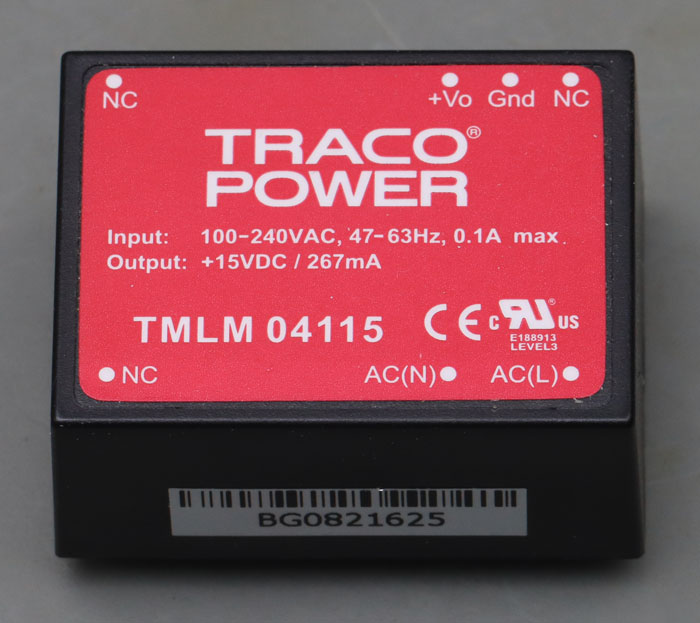
Traco Power manufactures various AC/DC and DC/DC converters, which are generally known for good quality. The TMLM series has a wide range input (90-246VAC) and offers output powers between 4W and 20W. The TMLM04115 generates 15V with a power handling capacity of 267mA. Efficiency is rated at 74%. Dimensions are 36,5mm x 27mm x 17,1mm.

The model here is a relatively early failure. It has blown a upstream 1A fuse.


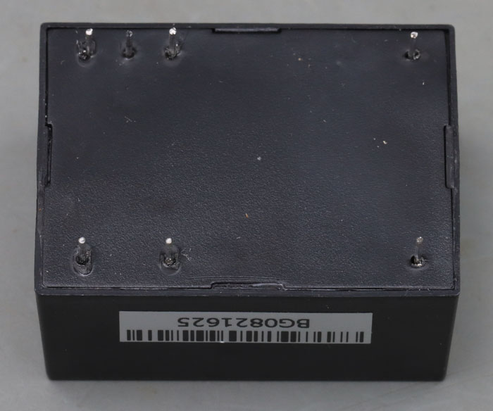
The case has seven pins, two of which only serve to stabilize the module. The switching regulator is located in a plastic cup that has been potted and closed with a lid on the bottom.


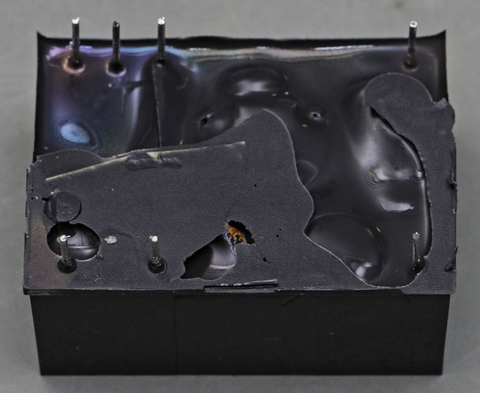
The silicone-like potting can be removed easily. The high packing density of the components is immediately noticeable.


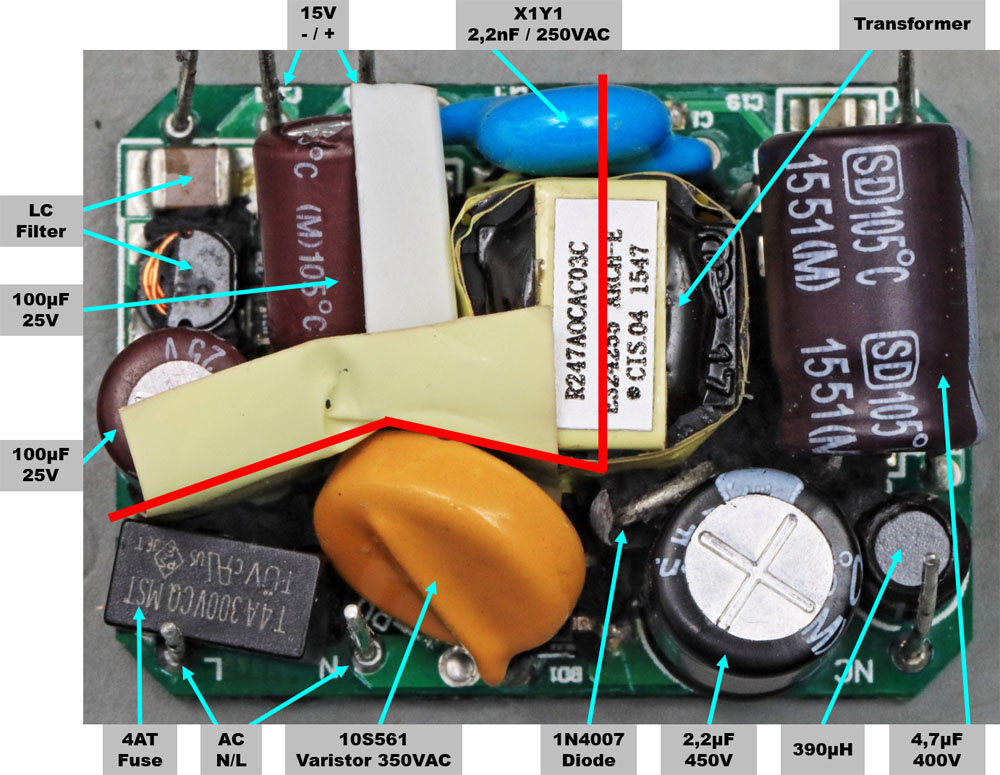
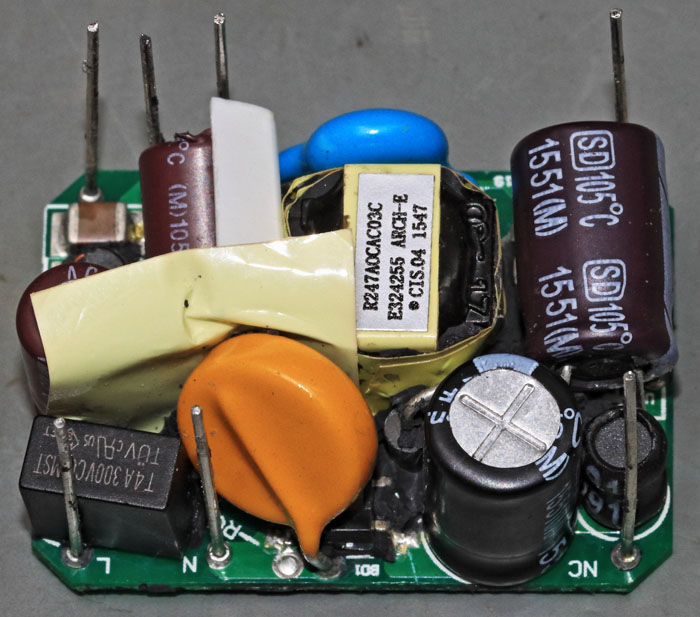
The galvanic isolation between the mains voltage and the output voltage is clearly visible. In the lower and right area are the circuit parts that work with mains voltage. In the upper left corner the low voltage part is built up. The isolation section is bridged in the middle by a transformer and a blue Y1 capacitor.

Since the input and output circuits are directly next to each other at the left edge, an additional foil had to be inserted here for isolation. To the left of the transformer, a plastic element has been inserted, whose function is not quite clear. The transformer itself seems to be sufficiently insulated. Maybe the plastic element guarantees a minimum distance to the Y1 capacitor.


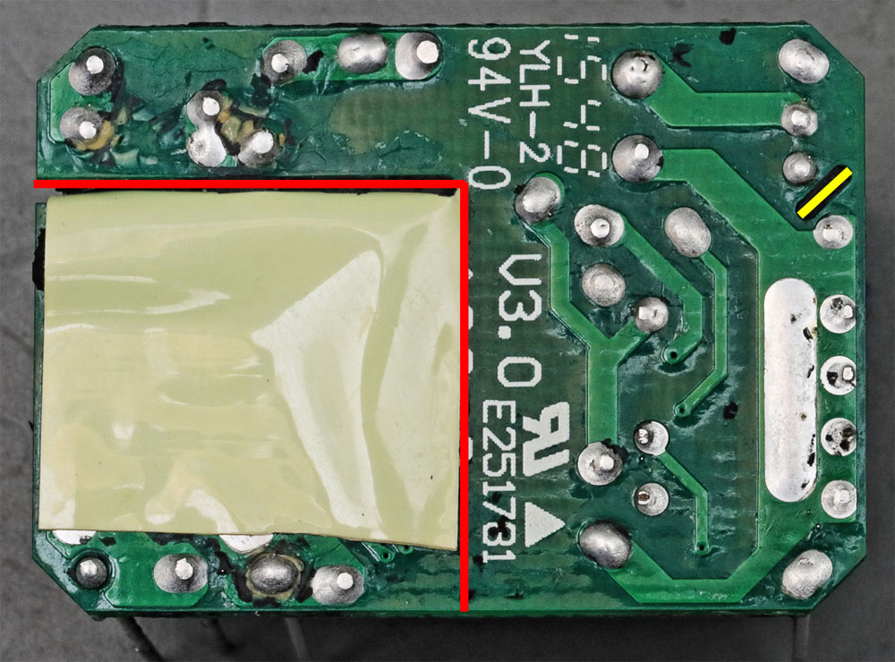
On the bottom side of the board, the foil for isolating the mains voltage has been glued to the low voltage area. At the right edge the potentials of the mains voltage are so close to each other that a slot had to be milled into the board.


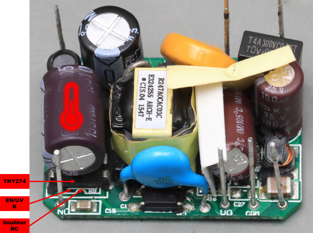
If you remove the large elements, the lower components become visible. The damage to the inductor in the upper left corner was done while removing the potting.


Underneath the insulation foil, it shows that the PCB was manufactured by the Chinese manufacturer YLH Electronics.


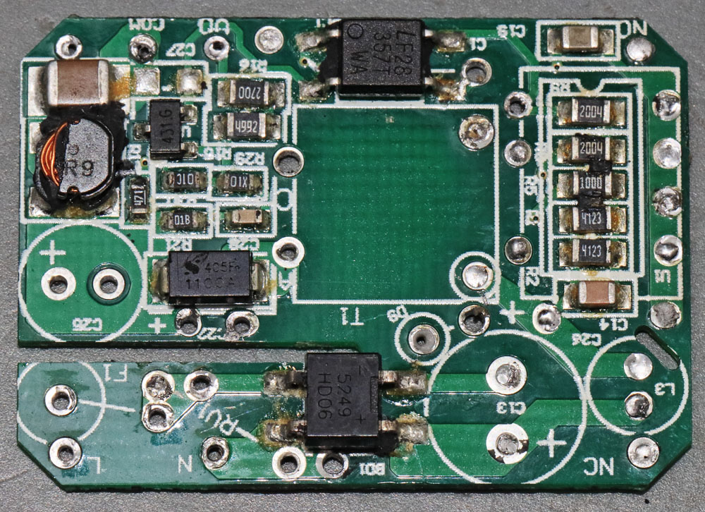
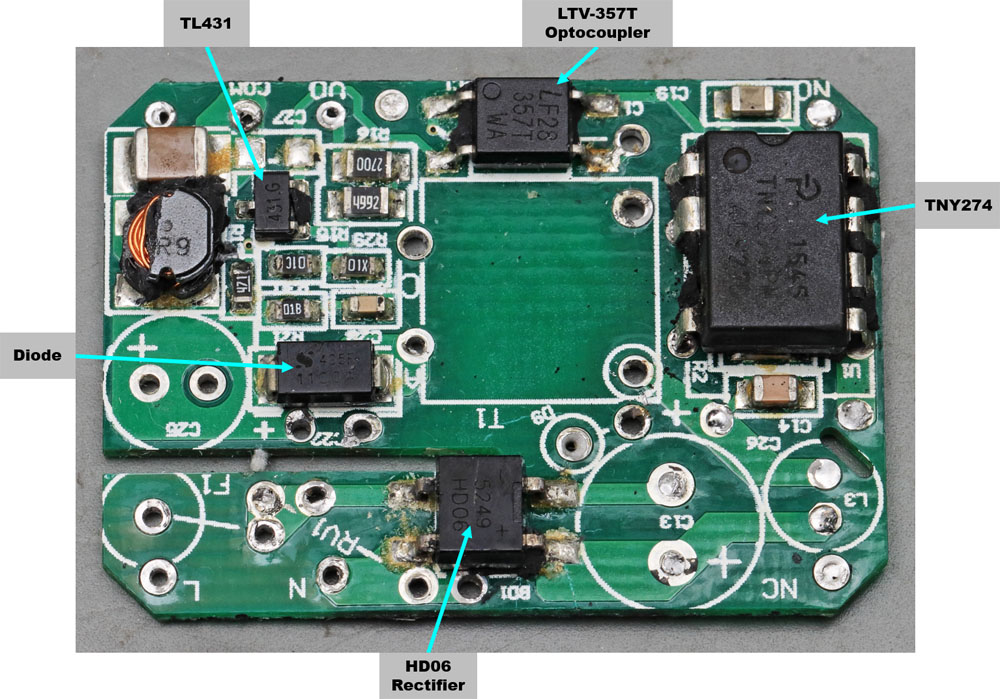
The last components only become visible when the TNY274 is desoldered. Five resistors are soldered under this component.


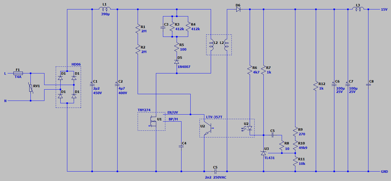
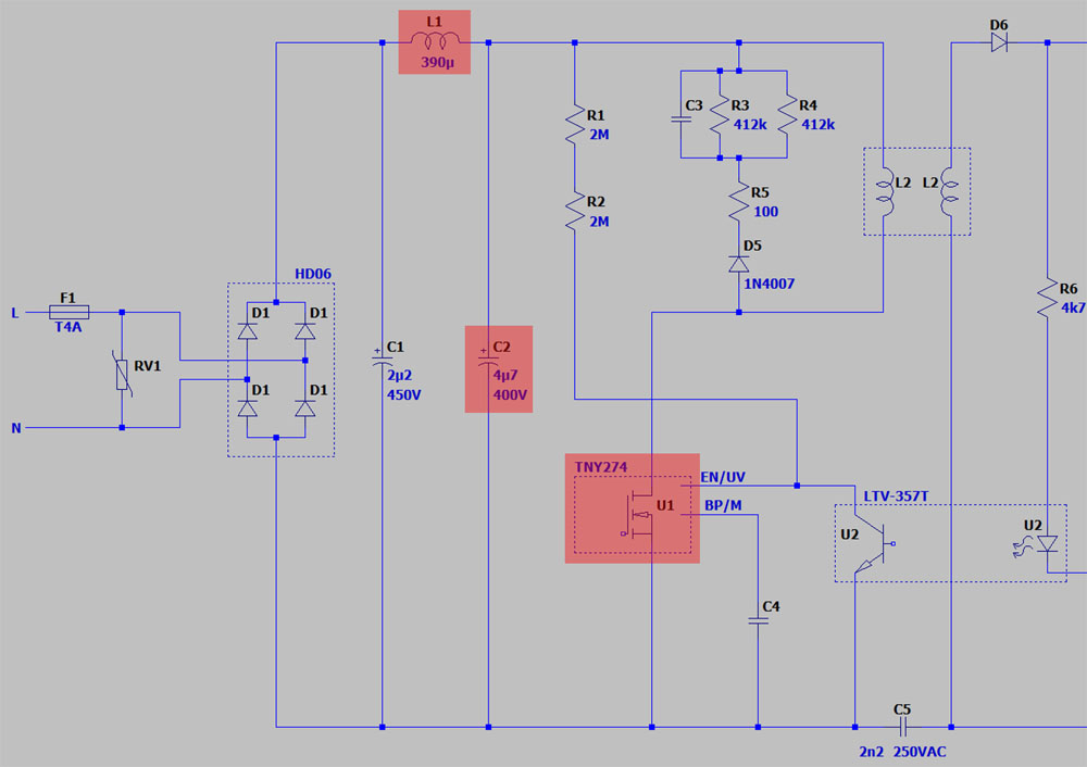
The circuit is not too complex. It is a typical flyback converter. Although the datasheet calls for a 3,15A slow-blow fuse externally, there is an additional 4A slow-blow fuse at the input. This is followed by a 350VAC varistor to protect against overvoltage pulses. The HD06 bridge rectifier safely blocks up to 600V.

On the primary side, two electrolytic capacitors are found, separated by a 390µH inductor. C1 is mainly used for smoothing the rectified line voltage. C2, as an intermediate circuit capacitor, supplies the current peaks that the switching regulator absorbs. The inductance L1 ensures on the one hand that the capacitor C1 is not loaded with the fast current changes and reduces on the other hand the emission of noise into the supply network.

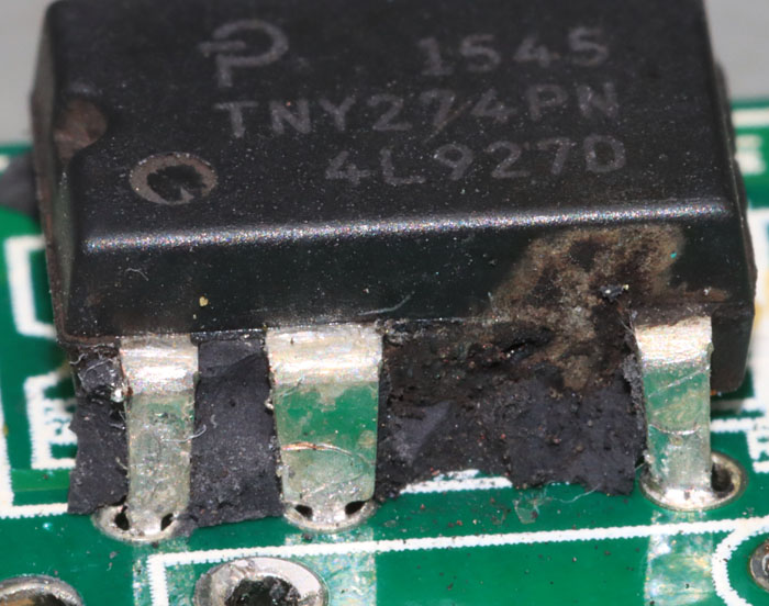
The TNY274 is a switching regulator that contains not only the controller but also the power transistor. It is from Power Integrations' TinySwitch-III family. Its clock frequency is 132kkHz. According to the datasheet, it can provide up to 5W of output power in a sealed package. Parallel to the primary coil of the transformer is the snubber circuit C3/R3/R4/R5/D5, which reduces the voltage peaks when the power transistor is switched off.

The transformer has just two windings. The TNY274 supplies itself directly from the power circuit, more precisely from its drain pin. An internal voltage regulator charges capacitor C4. While the power transistor is active, it serves as energy storage.

On the secondary side, rectification is done via D6. The capacitors C6/C7 absorb the energy packets and thus ensure a smoothed output voltage. The LC filter L3/C8 reduces the emission of high-frequency noise. Resistor R12 provides a minimum load so that the module operates stably even in no-load operation.

The output voltage is compared with the reference voltage of a TL431 shunt regulator. The voltage divider R9/R10/R11 defines the reference voltage. The RC element R8/C5 optimizes the behavior of the circuit at high frequencies. The magnitude of the output voltage defines the current through the LTV-357T optocoupler, which is the feedback of the switching regulator. Through the resistors R1/R2 the switching regulator monitors the mains voltage so that it can switch off in case of undervoltage.


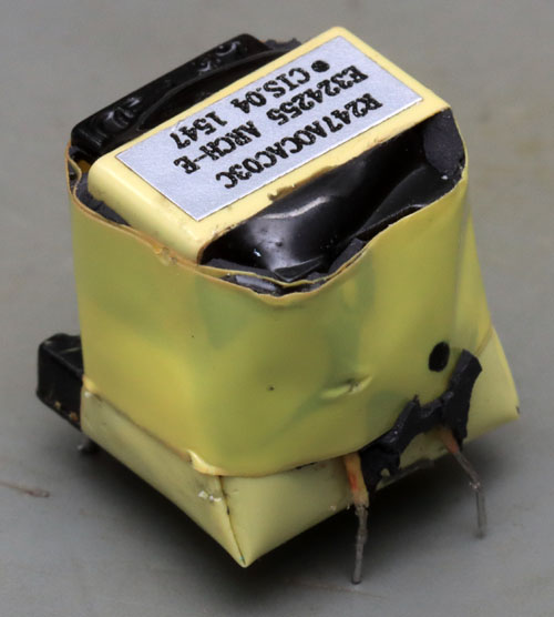
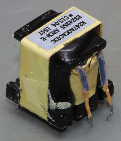
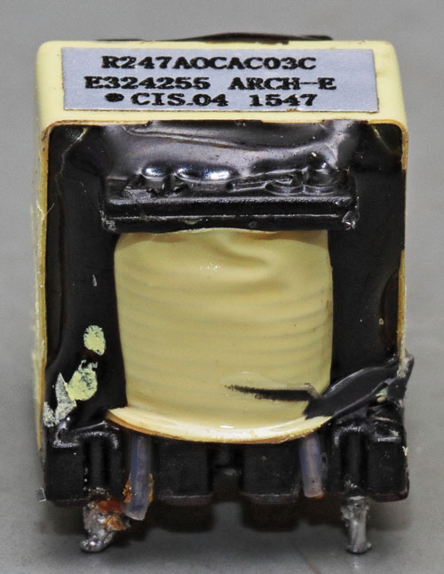
The transformer itself is potted with a hard black compound. The thicker leads of the secondary side were guided through the plastic body and fix the transformer to the PCB. The thin wires of the primary side run through the transformer body to the PCB without any guide. The wires from the primary and secondary sides are additionally insulated with tubing. The distance and the additional insulation are necessary to be able to represent the reinforced insulation against the mains voltage.


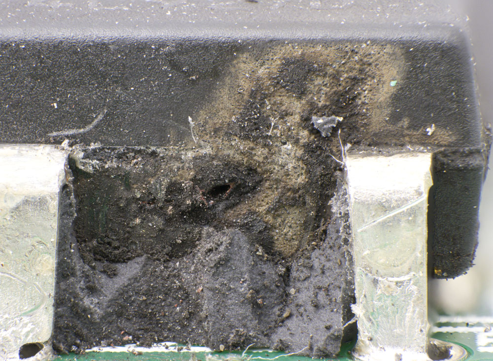
A closer look reveals that the switching regulator is definitely destroyed. A hole has burned into the side of the case and the surface of the case shows traces of a plasma.


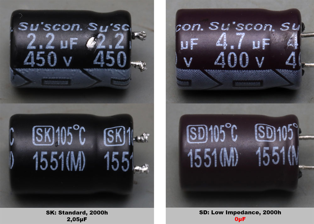
Two different electrolytic capacitors from the Taiwanese company Su'scon are used on the primary side. The less heavily loaded capacitor, which is mainly responsible for smoothing the rectified mains voltage, is one of the standard SK series capacitors. Directly on the switching regulator is an SD type with a reduced internal resistance. The lifetime of both types is specified at 2000 hours (at maximum current and temperature load). On the output side, on the other hand, there are KY capacitors from Nippon Chemi-Con with a estimated lifetime of 5000h.

It turns out that the capacitor on the switching regulator no longer offers any capacity at all.


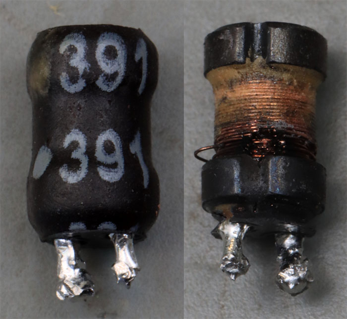
The inductance between the two electrolytic capacitors is defective too. This becomes clear when you remove the heat shrink tubing.


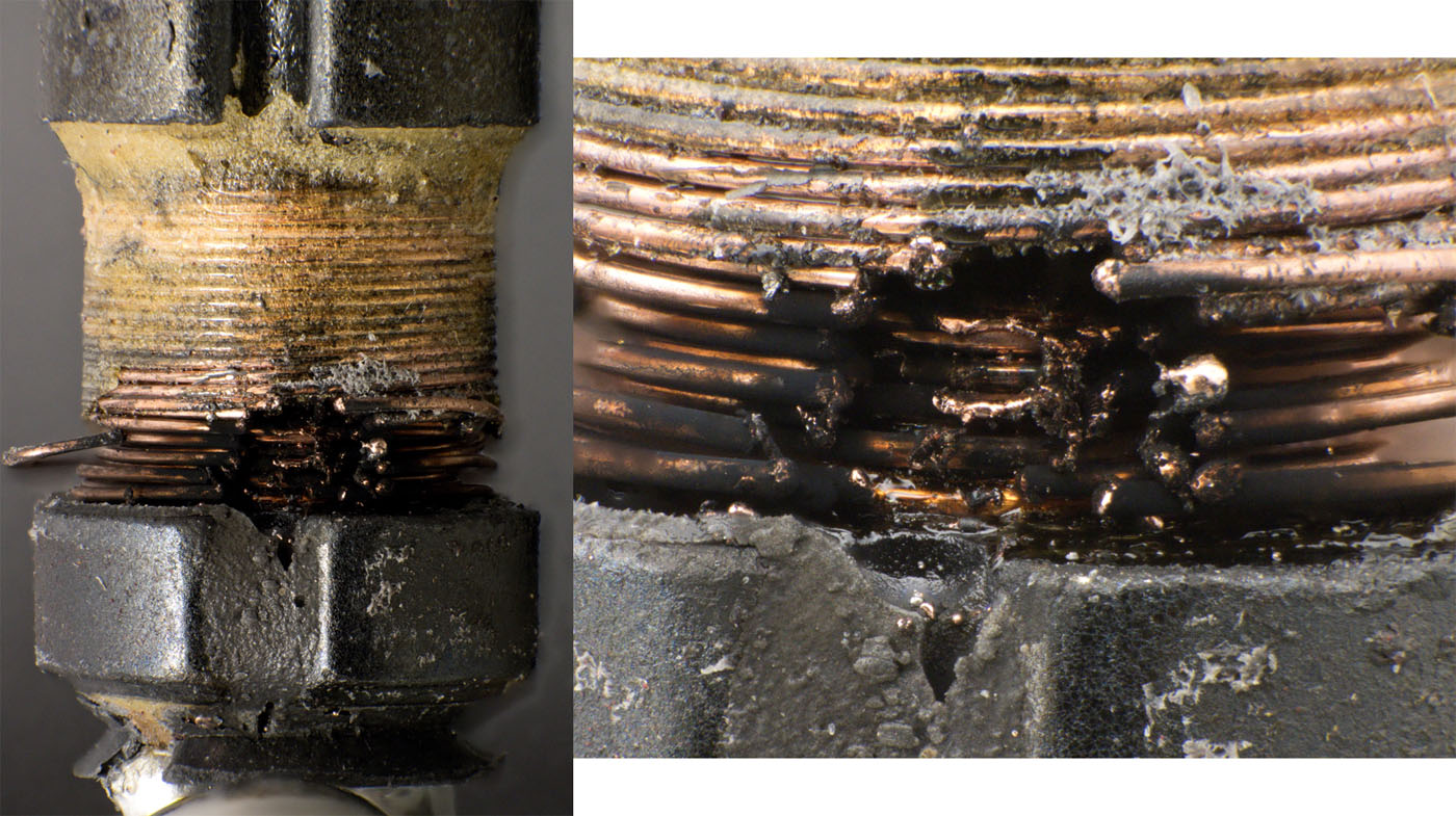
Where normally the wire of the inductor is led to the pin on the bottom side, a massive damage shows up. Several turns have melted open.


The damage of the inductance L1 could be caused by the defect of the switching regulator U1. However, this does not explain the missing capacitance of capacitor C2. It seems most likely that this capacitor was the starting point of the damage. Without sufficient capacitance at the input of the switching regulator, its supply voltage fluctuates very strongly. The inductance L1 can then even generate overvoltages. It was probably this instability that caused the switching regulator to be overloaded and eventually destroyed. The short circuit in the switching regulator then led to an overload of the inductance L1. It is quite possible that this was already overloaded before, because without the capacitor C2 much stronger current fluctuations had to be supplied from the capacitor C1. However, the inductance L1 did not interrupt the current flow like a fuse. This is shown by the many melted windings. In the end, the external fuse tripped.


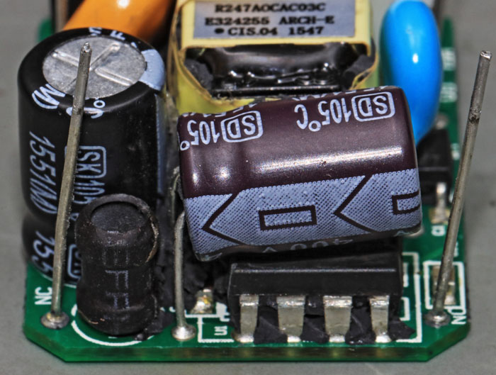
If you look at the setup, it's not surprising that capacitor C2 finally led to the defect of the module. It is located directly above the switching regulator, which according to the datasheet can reach temperatures of up to 110°C at its pins. In addition to the power dissipation of the switching regulator, there is also the power dissipation of the components underneath the module (voltage measurement and snubber). The maximum permissible operating temperature of the capacitor, on the other hand, appears to be very low at 105°C, since it is also subject to a certain amount of self-heating due to its current load. The relatively short specified lifetime of 2000 hours in combination with the high load then ensures early failures.

The TNY274 datasheet specifies a rated power of 5W when used in a sealed enclosure. Traco Power specifies the TMLM family at only 4W. The reason for this is probably the limited and encapsulated installation space, which makes heat dissipation more difficult. The maximum operating temperature of the TMLM modules, which is only 60°C, also shows how critical this point is.


https://www.richis-lab.de/TMLM04115.htm

 :-/O


...you are right, there is no die picture...  ;D
 
The following users thanked this post: SeanB, doktor pyta, RoGeorge, MegaVolt

Online RoGeorge

  • Super Contributor
  • ***
  • Posts: 6203
  • Country: ro
Re: Voltage regulators - die pictures
« Reply #124 on: March 25, 2023, 03:39:20 pm »
there is no die picture...  ;D

...only "when regulators die" pictures.  8)

Offline NoopyTopic starter

  • Super Contributor
  • ***
  • Posts: 1735
  • Country: de
    • Richis-Lab
Re: Voltage regulators - die pictures
« Reply #125 on: March 25, 2023, 04:10:41 pm »
there is no die picture...  ;D

...only "when regulators die" pictures.  8)

Since I'm not a native speaker that should be enough.  :-+ ;D

Offline T3sl4co1l

  • Super Contributor
  • ***
  • Posts: 21688
  • Country: us
  • Expert, Analog Electronics, PCB Layout, EMC
    • Seven Transistor Labs
Re: Voltage regulators - die pictures
« Reply #126 on: March 25, 2023, 06:25:33 pm »
Agree with the failure analysis. :-+

Resistors under the chip, damn, talk about desperate for space! :-DD

Funny enough, I had a similar failure mechanism on an LED lamp I made some years ago.  The main filter cap (47uF 160V I think; 120V single phase only, so this is fine) apparently failed by leakage and corrosion (perhaps it wasn't in great shape to start, perhaps it was installed with too much lead strain; I don't recall it ran hot though), and the failure mechanism leading up to the fault was a noisy and intermittent operation.  The lead corroding off is equivalent to it drying up to ~zero value, and cascading failure ensued (switch avalanche + destruction, controller taken out by backflow from gate pin); and I think that was all that failed, maybe some passives?).  Replaced the relevant parts and good as new, of course.  With a brand new cap (and minimal lead strain) this time. :P

Tim
Seven Transistor Labs, LLC
Electronic design, from concept to prototype.
Bringing a project to life?  Send me a message!
 
The following users thanked this post: Noopy

Offline floobydust

  • Super Contributor
  • ***
  • Posts: 7007
  • Country: ca
Re: Voltage regulators - die pictures
« Reply #127 on: March 25, 2023, 06:28:29 pm »


It appears made by Arch Electronics Taiwan with Traco handling UL certification.
I would make sure the transformer isolation is intact, take it apart like DiodeGoneWild does on his Youtube channel. The DC inductor fail melted turns mean a lot more current than this PSU can put out, came from somewhere.
edit: it's the inductor on the primary-side that fused.

I have found with the Taiwan and china power supply OEM's that they play a game with the quality of the electrolytics. You are given "golden samples" and later the cheap parts come in, and you can't tell because it's all potted. I had some defective due to the transformer being wound incorrectly. It's all good and quiet until you take it apart lol.
« Last Edit: March 25, 2023, 07:11:04 pm by floobydust »
 
The following users thanked this post: SeanB, exe

Offline magic

  • Super Contributor
  • ***
  • Posts: 6779
  • Country: pl
Re: Voltage regulators - die pictures
« Reply #128 on: March 25, 2023, 06:45:18 pm »
The damage of the inductance L1 could be caused by the defect of the switching regulator U1. However, this does not explain the missing capacitance of capacitor C2. It seems most likely that this capacitor was the starting point of the damage. Without sufficient capacitance at the input of the switching regulator, its supply voltage fluctuates very strongly. The inductance L1 can then even generate overvoltages.
U1 and L1 make a nice little boost converter here >:D

...you are right, there is no die picture...  ;D
I counted two ICs on this board, so maybe...
 :popcorn:
 

Offline NoopyTopic starter

  • Super Contributor
  • ***
  • Posts: 1735
  • Country: de
    • Richis-Lab
Re: Voltage regulators - die pictures
« Reply #129 on: March 25, 2023, 07:59:01 pm »
It appears made by Arch Electronics Taiwan with Traco handling UL certification.

The Arch power modules look similar. But is there something that makes you sure the TRACO is a Arch module?


I would make sure the transformer isolation is intact, take it apart like DiodeGoneWild does on his Youtube channel. The DC inductor fail melted turns mean a lot more current than this PSU can put out, came from somewhere.
edit: it's the inductor on the primary-side that fused.

I agree with you. I was able to measure a resistance and an inductance but didn´t check it in detail.
My transformer is potted with some hard material. I will try to remove it to take a closer look.


U1 and L1 make a nice little boost converter here >:D

Oh yes...  >:D


I counted two ICs on this board, so maybe...
 :popcorn:

Of course they are in the waiting list.  ;D
Damaged parts can give interesting pictures... ...if they don´t fall apart while decapping.

Offline floobydust

  • Super Contributor
  • ***
  • Posts: 7007
  • Country: ca
Re: Voltage regulators - die pictures
« Reply #130 on: March 25, 2023, 08:15:52 pm »
It appears made by Arch Electronics Taiwan with Traco handling UL certification.
The Arch power modules look similar. But is there something that makes you sure the TRACO is a Arch module?
It's the label on the transformer "ARCH" and the file numbers.
There is no inrush PTC so they must use a very big fuse which can have bad consequences. MST T4A is a slow-blow fuse, 4*In (=16A) 0.15-3 seconds, a bit much for this.
 
The following users thanked this post: Noopy

Offline NoopyTopic starter

  • Super Contributor
  • ***
  • Posts: 1735
  • Country: de
    • Richis-Lab
Re: Voltage regulators - die pictures
« Reply #131 on: March 25, 2023, 08:29:06 pm »
Indeed, I didn´t see the "ARCH-E" on the transformer.  :-+

Yes, it´s really a big fuse for that small power module.

Offline AnalogTodd

  • Regular Contributor
  • *
  • Posts: 89
  • Country: us
Re: Voltage regulators - die pictures
« Reply #132 on: March 25, 2023, 09:30:36 pm »
Just found this thread. Think I'll have to keep an eye on it, considering it covers the job I did for a lot of years...
Lived in the home of the gurus for many years.
 

Offline NoopyTopic starter

  • Super Contributor
  • ***
  • Posts: 1735
  • Country: de
    • Richis-Lab
Re: Voltage regulators - die pictures
« Reply #133 on: March 25, 2023, 09:49:51 pm »
Just found this thread. Think I'll have to keep an eye on it, considering it covers the job I did for a lot of years...

If you are interested in more die pictures just look at my other topics...

Offline AnalogTodd

  • Regular Contributor
  • *
  • Posts: 89
  • Country: us
Re: Voltage regulators - die pictures
« Reply #134 on: March 25, 2023, 10:01:15 pm »
I've looked through those as well. To me, the voltage regulators is a special one since that was what I designed for a lot of years.
Lived in the home of the gurus for many years.
 

Offline exe

  • Supporter
  • ****
  • Posts: 2563
  • Country: nl
  • self-educated hobbyist
Re: Voltage regulators - die pictures
« Reply #135 on: March 26, 2023, 06:03:54 am »
I've looked through those as well. To me, the voltage regulators is a special one since that was what I designed for a lot of years.

Can you disclose which regulators you designed?
 

Offline AnalogTodd

  • Regular Contributor
  • *
  • Posts: 89
  • Country: us
Re: Voltage regulators - die pictures
« Reply #136 on: March 26, 2023, 02:37:10 pm »
A good portion of the LTC portfolio is mine. All of the LT176X linear regulators, LT3080 family, LT3093, LT3094, and others.
« Last Edit: March 26, 2023, 02:39:01 pm by AnalogTodd »
Lived in the home of the gurus for many years.
 
The following users thanked this post: exe, RoGeorge, Zoli

Offline magic

  • Super Contributor
  • ***
  • Posts: 6779
  • Country: pl
Re: Voltage regulators - die pictures
« Reply #137 on: March 26, 2023, 08:27:33 pm »
That's some good stuff :-+
(Still curious how those precision rail-to-rail current sources work...)
 

Offline AnalogTodd

  • Regular Contributor
  • *
  • Posts: 89
  • Country: us
Re: Voltage regulators - die pictures
« Reply #138 on: March 26, 2023, 09:52:25 pm »
Smoke and mirrors. Which is why they stop working when someone lets the smoke out...

Technically, what we do is create a voltage that has a flat characteristic across temperature and drop it across a resistor. Set things up right and it only takes a couple hundred millivolts of headroom to run from the rail (though the bulk of the circuit takes a couple volts to run from VIN to GND).
Lived in the home of the gurus for many years.
 

Offline exe

  • Supporter
  • ****
  • Posts: 2563
  • Country: nl
  • self-educated hobbyist
Re: Voltage regulators - die pictures
« Reply #139 on: March 27, 2023, 06:37:36 pm »
LT3080 family

Oh, those are my favorite)
 

Offline AnalogTodd

  • Regular Contributor
  • *
  • Posts: 89
  • Country: us
Re: Voltage regulators - die pictures
« Reply #140 on: March 28, 2023, 07:58:20 pm »
The Linear Technology LT3750...


We had this strange NPN transistors in the LT3750.


I found a good explanation for these structures in the book "The Art of Analog Layout" by Alan Hastings.

The basis is a so-called CDI bipolar transistor, as it is common in a BiCMOS process. CDI stands for "collector diffused isolation" and describes the isolation of the transistor from its environment by an n-doped well within the p-doped epitaxial layer. The special feature is the emitter, which is created by applying a heavily n-doped polysilicon layer over an oxide mask and allowing its doping to diffuse into the base surface.

A transistor constructed in this way has a small emitter with high doping. The base area can also be made more highly doped and thinner. All this has a positive effect on the transistor's properties. Current gain and switching frequency are very high.

Consequently, the dark areas of the transistors are the openings where the red polysilicon layer forms the emitter surfaces. Whether this is really a BiCMOS process remains questionable, since no MOSFETs can be seen in the whole circuit. Nevertheless, the emitters can be represented by a polysilicon layer.


https://www.richis-lab.de/voltageregulator18.htm#Poly-Emitter

 :-/O
That is a correct description of these devices. The interesting bit is when you look at some of them where the contact is directly over the emitter, but there are others where it appears contacts are not over the emitters. This was done to promote matching of devices; a contact directly in the emitter region could cause defects that contributed to mismatch, but use the conductive poly to bring the emitter connection out and away and you get better results.
Lived in the home of the gurus for many years.
 
The following users thanked this post: SeanB, RoGeorge, floobydust, Noopy

Offline NoopyTopic starter

  • Super Contributor
  • ***
  • Posts: 1735
  • Country: de
    • Richis-Lab
Re: Voltage regulators - die pictures
« Reply #141 on: March 28, 2023, 08:00:12 pm »
Very interesting! Thanks for providing this information!  :-+

Offline NoopyTopic starter

  • Super Contributor
  • ***
  • Posts: 1735
  • Country: de
    • Richis-Lab
Re: Voltage regulators - die pictures
« Reply #142 on: May 30, 2023, 06:50:50 pm »


The Taiwanese company Holtek is best known for its microcontrollers. Holtek works fabless. This means that they do not have any production lines themselves. Holtek develops circuits and then has them produced by contract manufacturers (foundries) such as TSMC.

The HT7530-1 is a 3V voltage regulator that can deliver up to 100mA. The SOT89 package allows a power dissipation of up to half a watt. The maximum allowable input voltage is 30V. Without any load the HT7530 draws just 2,5µA. 15 alternative variants of the voltage regulator provide surprisingly finely graded output voltages between 2,1V and 15V. The initial accuracy is +/-3%. The temperature drift is given as 100ppm/°C. As a low-drop voltage regulator, the minimum required voltage drop across the device is typically just 30mV (at 1mA).


The datasheet describes that the HT7530 is based on a CMOS process. A relatively simple block diagram is also shown there.


The dimensions of the die are 0,46mm x 0,41mm. Although the structures are very small, you can still make out the functional blocks. The large evenly structured area contains the power transistor. As usual for a power MOSFET, the transistor consists of many small cells. Accordingly, the bondpads in the upper corners must be the input and the output of the regulator. Thus, the lower bondpad on the left edge must be the contact for the reference potential.

In the lower area, five testpads are placed, between which you can make out fuses. Below the testpads, a whole row of resistors extend from the left to the right edge. On the right edge there is another testpad that seems to operate a fifth fuse in the lower area. Either the output voltage is adjusted with these structures or the voltage regulator can initially display all output voltages listed in the datasheet and one of them is selected via the testpads. The relatively high tolerance of +/-3% speaks for the second possibility. Due to the partly small gradations of the possible output voltages, it is possible that both a selection of the output voltage and a certain adjustment is possible via the fuses.

The rest of the circuit is between the power transistor and the testpads. In fact, it seems to be only a few elements. In this case, the block diagram is probably not oversimplified.


https://www.richis-lab.de/voltageregulator21.htm

 :-/O
 
The following users thanked this post: SeanB, exe, RoGeorge, floobydust, MegaVolt

Offline NoopyTopic starter

  • Super Contributor
  • ***
  • Posts: 1735
  • Country: de
    • Richis-Lab
Re: Voltage regulators - die pictures
« Reply #143 on: November 17, 2023, 08:26:17 pm »


The LM125 is a voltage regulator with two output voltages, +15V and -15V. In addition to the LM125, which is specified for an operating temperature range of -55°C to 125°C, National Semiconductor also sold the LM325, which is specified to operate between 0°C and 70°C. The same datasheet also includes the LM126 and LM326, which supply output voltages of -12V and 12V. The maximum input voltage is +/-30V. The maximum output current is 100mA. Overcurrent protection typically kicks in at 260mA.


The circuit diagram in the datasheet is rather confusing at first glance.


In contrast, the description of the LM125 in Application Note 82 from National Semiconductor is much easier to understand and very detailed (https://www.richis-lab.de/images/vreg/24x05.pdf). The block diagram you see here provides an overview. The reference voltage is generated on the negative side. The resistors Ra and Rb define the output voltage. The positive voltage regulator uses the negative output voltage as a reference. If the negative voltage rises, the positive voltage falls accordingly. For this reason, the LM125 is also referred to as a "tracking regulator". The resistors Rc and Rd define the output voltage on the positive side.


The dimensions of the die are 2,3mm x 1,6mm. The large output stage transistors are clearly visible on the right and left edges. Some resistors with additional contacts have been integrated in the center of the die. These are probably the feedback resistors Ra to Rd and the additional contacts make it possible to switch from 15V to 12V with a simple change of the metal layer.


https://www.richis-lab.de/voltageregulator22.htm

 :-/O
 
The following users thanked this post: SeanB, RoGeorge

Offline NoopyTopic starter

  • Super Contributor
  • ***
  • Posts: 1735
  • Country: de
    • Richis-Lab
Re: Voltage regulators - die pictures
« Reply #144 on: January 08, 2024, 04:40:15 am »


The SG3532 voltage regulator is very similar to the LM723 (https://www.richis-lab.de/LM723.htm). Silicon General advertises the wider operating voltage range, which extends from 4,5V to 50V. In addition, there is overcurrent protection in the power path and at the reference output, overtemperature protection and a pin with which the voltage regulator can be deactivated. The SG3532 allows an output current of up to 250mA.

Only the SG1532 and SG2532 variants allow the full 50V. The SG3532 is only approved for 40V. These appear to be different bins. The SG1532 also offers an extended operating temperature range of -55°C to 125°C.


The circuit diagram in the datasheet shows a similar, but slightly different circuit compared to the LM723. The SG3532 uses a bandgap reference.


The dimensions of the die are 1,7mm x 1,5mm. The letters CG in the upper left corner could be the initials of a developer. The numbers 1532 stand for the variant SG1532.


The datasheet contains an illustration of the metal layer. This shows that the layout has been revised at least once. The structure is apparently basically the same, but some structures have changed in the left-hand area.


Test structures of eight masks are shown in the bottom left-hand corner, which allow the exposure performance of the process to be evaluated.


https://www.richis-lab.de/voltageregulator23.htm

 :-/O
 
The following users thanked this post: SeanB, RoGeorge, ch_scr, D Straney

Offline NoopyTopic starter

  • Super Contributor
  • ***
  • Posts: 1735
  • Country: de
    • Richis-Lab
Re: Voltage regulators - die pictures
« Reply #145 on: January 10, 2024, 07:27:27 pm »


I have taken a closer look at the circuit. You can see that it largely corresponds to the circuit in the datasheet. Some resistors, mainly emitter resistors, have not been included and the bias circuit is slightly different. An additional transistor has been integrated at the current mirror around Q15, which supplies the base currents for the current sources. The current mirror around Q22 is also somewhat more complex.

Two bondpads are provided for the shutdown pin, as it is led out at a different point in the TO package than in the DIL package. The capacitor C1 uses two capacitances. Under the upper electrode, built in the metal layer, the barrier layer of a base-emitter structure provides an additional high capacitance. The transistor Q29 has an unusual structure. The area between the base and collector has been enlarged and structured so that an additional capacitance is created there.


Now let´s take a second look at the metal layer in the datasheet. Presumably it is the current sources that have been revised and no longer fully correspond to the circuit diagram. The overcurrent protection with Q29 does not seem to have had any capacity in this revision.


https://www.richis-lab.de/voltageregulator23.htm#schematic

 :-/O
 
The following users thanked this post: SeanB, RoGeorge, ch_scr

Offline NoopyTopic starter

  • Super Contributor
  • ***
  • Posts: 1735
  • Country: de
    • Richis-Lab
Re: Voltage regulators - die pictures
« Reply #146 on: February 18, 2024, 05:32:20 am »


The Fairchild µA78HG voltage regulator is shown here in the original packaging. The H in the designation shows that it is a hybrid component. There is a note on the back that the package contains beryllium oxide and that the voltage regulator should therefore be returned to Fairchild for fault analysis.

With an input voltage of up to 40V, the output voltage of the µA78HG can be set between 5V and 24V via a voltage divider. The output current is specified with a maximum of 5A. The short-circuit protection typically kicks in at 7A. Up to 50W can be dissipated.


The µA78HG is housed in a TO-3 package. This is the historical widespread variant with a very thick base plate. As the component has four potentials to the outside, the TO-3 variant with four pins was selected. Numbers help to identify the pins. The base plate is flattened on one side so it´s easier to mount the regulator in the right orientation.


The housing contains a ceramic carrier on which an integrated circuit and a power transistor are placed. A clear encapsulation protects the semiconductors.


The transistor has a MESA structure. The edge length is 3,0 mm. The thick bondwire conducts the supply potential coming from the left hand side. The base area is contacted with a thin bondwire. The fact that the supply potential contacts the emitter area shows that it is a PNP transistor.


There is an L-shaped structure on the lower edge. This can be used to check how well the masks were aligned during production.


The integrated circuit contains the regulator. The dimensions of the die are 1,8mm x 1,9mm.


The designation 78DHZ is shown in the metal layer on the left side of the die.


The Fairchild Voltage Regulator Handbook from 1978 contains a block diagram for the µA78HG. The integrated part is labelled as µA78M00. The µA78M00 itself is already a complete voltage regulator. The external elements merely extend the current carrying capability and realise overcurrent protection in this path.

As will be shown later, the representation of the external component does not match the µA78HG documented here. The series regulator transistor and its shunt are actually external. However, the µA78M00 is responsible for detecting and switching off the overcurrent. For this just a small modification of the metal layer was necessary. Perhaps there was an earlier revision in which the µA78M00 regulator was an unmodified voltage regulator and all the elements seen here had to be integrated externally.


A detailed circuit diagram of the µA78M00 is also documented in the Fairchild Voltage Regulator Handbook. The Siemens TDB7805 has the same structure. The functionality of the circuit is described there in more detail (https://www.richis-lab.de/voltageregulator05.htm). However, here a fixed-voltage version without the modification for use with an external series regulator is shown. A µA78M05 with an output voltage of 5V would look like this, for example. The voltage divider for the feedback is integrated in these regulators (R19/R20).


Most of the circuit can be found on the die. The transistor Q14, which represents the overtemperature protection, is designed as a Darlington pair. The DR14 diode can be found in the reference voltage path. This may have reduced the temperature drift even further.


As already described, the µA78M00 has been modified for use with an external transistor. To make the differences clear, the circuit diagram from the Fairchild Voltage Regulator Handbook has been adapted accordingly. The control potential is brought out so that the output voltage can be set externally. The shunt R11 is missing, instead the potential Output R11 is led out, with which an external current limitation can be set up. In addition, the collector of transistor Q17 can be contacted exclusively. This transistor itself represents the series regulator in the original circuit. Isolated from the input voltage, however, it can also be used as a driver for a PNP transistor.


There are two resistors at the lower edge of the die, which can represent the voltage divider for the feedback as R19 and R20 in the fixed-voltage variants. R20 consists of several small elements so that the different output voltages can be set.


Changing the metal layer is sufficient to integrate the voltage divider for the output voltage into the circuit. The same applies to the integrated series regulator and the shunt R11. In the µA78HG (left), R11 is wired as the emitter resistor of Q15. Its influence in the circuit should not be too great. For applications without an external control transistor, R11 can be integrated as a shunt by making small changes to the metal layer (right). The bondpad OUT R11 is then no longer used. The line to the upper bondpad appears very thin for the output current of 500mA. It may need to be widened to the left. The adjacent GND line is redundant.


There is a line on the ceramic carrier that serves as the shunt resistor Rh for overcurrent protection.


Somewhat later, another variant of the voltage regulator was introduced with the designation µA78HGA. This does not appear to be just a bin. The A variant is explicitly advertised as pin-compatible.


The µA78HGA datasheet shows a photo of the internal structure. The quality of the photo is very poor, but it appears to show a different structure compared to the regulator shown here. However, it does not necessarily have to be the A variant. It is also conceivable that the picture is just an example and that the first revision with the external current limiter is shown.


https://www.richis-lab.de/voltageregulator24.htm

 :-/O
 
The following users thanked this post: SeanB, Vgkid, doktor pyta, exe, RoGeorge, iMo, D Straney

Offline NoopyTopic starter

  • Super Contributor
  • ***
  • Posts: 1735
  • Country: de
    • Richis-Lab
Re: Voltage regulators - die pictures
« Reply #147 on: February 18, 2024, 12:27:27 pm »
I have updated the last picture, the datasheet of the A variant (due to hotlinking the upper post is updated).

There you can see they changed the shunt to a thick film resistor. Perhaps that was the change of the A variant.

Someone gave me the hint that in the second line of the marking there is an A and perhaps that is already the A variant. Well it´s possible but the ending "HGAKC" wouldn´t fit to the datasheet. A year before there was no A variant. The first announcement of the A variant I found was 1982.
Well, I´m not sure and will have to take a closer look...

Offline MarkT

  • Frequent Contributor
  • **
  • Posts: 367
  • Country: gb
Re: Voltage regulators - die pictures
« Reply #148 on: February 18, 2024, 02:05:36 pm »
I am amused that 2.3V is touted as "low drop-out voltage".  According to semiconductor manufacturer's every voltage regulator is "low drop-out", like motor manufacturers' claim that every motor is "high torque".
 

Offline NoopyTopic starter

  • Super Contributor
  • ***
  • Posts: 1735
  • Country: de
    • Richis-Lab
Re: Voltage regulators - die pictures
« Reply #149 on: February 18, 2024, 02:13:55 pm »
2,3V is quite a voltage drop but back in the days that probably was not that bad.  :D
 
The following users thanked this post: SeanB

Offline SeanB

  • Super Contributor
  • ***
  • Posts: 16284
  • Country: za
Re: Voltage regulators - die pictures
« Reply #150 on: February 18, 2024, 05:54:15 pm »
Still might have some of those around as well. They were an interesting device for sure. And yes 2V3 was a low dropout voltage, especially when almost all the competition had an absolute minimum dropout of 3V0, and with that the caveat that PSRR would be worse at that voltage, that extra 700mV was a bonus, and also that PSRR was not affected. Meant you could supply a S100 bus card with a single TO3 package regulator on the card, and a smallish clip over heatsink, and still be able to have over 4A of current draw on the card. The alternative was to have a long aluminium strip on the side, and 4 TO220 voltage regulators taking up a good chunk of valuable real estate on the card.
« Last Edit: February 18, 2024, 05:57:57 pm by SeanB »
 
The following users thanked this post: RoGeorge, Noopy

Offline ArdWar

  • Frequent Contributor
  • **
  • Posts: 373
  • Country: sc
Re: Voltage regulators - die pictures
« Reply #151 on: February 18, 2024, 06:00:55 pm »
I am amused that 2.3V is touted as "low drop-out voltage".
This is still rather high even with the original definition of "less than a Darlington drop" hmmm.
 

Offline Gyro

  • Super Contributor
  • ***
  • Posts: 9507
  • Country: gb
Re: Voltage regulators - die pictures
« Reply #152 on: February 18, 2024, 06:25:19 pm »
Remember it was the 1970s and it was a 5A regulator - high for a linear regulator these days.
Best Regards, Chris
 
The following users thanked this post: SeanB

Offline SeanB

  • Super Contributor
  • ***
  • Posts: 16284
  • Country: za
Re: Voltage regulators - die pictures
« Reply #153 on: February 18, 2024, 07:07:04 pm »
Yes, and also the beryllia there is not pink, but white.
 

Offline Gyro

  • Super Contributor
  • ***
  • Posts: 9507
  • Country: gb
Re: Voltage regulators - die pictures
« Reply #154 on: February 18, 2024, 07:46:51 pm »
Yes, a good example for those who automatically interpret pink as Beryllium. I've seen plenty of Beryllium containing ceramic HF power transistors that were white. Low thermal resistance requirement is much more of a guide than color.
Best Regards, Chris
 

Offline quince

  • Newbie
  • Posts: 8
  • Country: de
Re: Voltage regulators - die pictures
« Reply #155 on: February 18, 2024, 08:13:03 pm »
Subscribing :)
 
The following users thanked this post: Noopy

Offline T3sl4co1l

  • Super Contributor
  • ***
  • Posts: 21688
  • Country: us
  • Expert, Analog Electronics, PCB Layout, EMC
    • Seven Transistor Labs
Re: Voltage regulators - die pictures
« Reply #156 on: February 18, 2024, 08:27:25 pm »
Where do people think BeO is pink?  Cr2O3 added to Al2O3 makes it pink.  Al2O3 doesn't need to be pink, it's used pure white often enough, but also often is made pink for vacuum tubes.

I still haven't seen anyone cite standards suggesting/dictating whether this is actually the case, and I haven't seen anything authoritative that suggests BeO was ever colored pink (and the exact shade of pink at that; I don't know if Cr2O3 has the same effect in BeO, or if another element could contribute a similar enough color to be confused with it).

Tim
Seven Transistor Labs, LLC
Electronic design, from concept to prototype.
Bringing a project to life?  Send me a message!
 

Offline NoopyTopic starter

  • Super Contributor
  • ***
  • Posts: 1735
  • Country: de
    • Richis-Lab
Re: Voltage regulators - die pictures
« Reply #157 on: February 18, 2024, 08:53:51 pm »
Where do people think BeO is pink?

Well there were rumors and rumors are often very famous...  ;D

Offline NoopyTopic starter

  • Super Contributor
  • ***
  • Posts: 1735
  • Country: de
    • Richis-Lab
Re: Voltage regulators - die pictures
« Reply #158 on: March 13, 2024, 03:03:30 am »


Now let´s go on with the µA78HG story. The µA78HG shown here was produced in 1980, one year after the µA78HG from 1979. Externally, there are no recognisable differences. But here we definitely have not an "A" version.


It can be seen that the voltage regulator is constructed in exactly the same way as the µA78HG from 1979, although a smaller transistor has been used here as a power transistor.


The edge length of the power transistor is 2,7 mm. It is a MESA transistor, but here not only the outer edges have been etched down, but a trench has been incorporated.


The controller itself does not differ from the µA78HG from 1979.


An artefact catches the eye at the bottom edge. There is dark material on a transistor. It does not appear to be electrical damage. This is contradicted by the loose structure on the surface of the semiconductor and the fact that the metallisation is still intact. It seems more likely that unclean processes have left "dirt" behind or that some kind of corrosion has occurred locally. This would also explain the blackened contact of the resistor placed next to it.


The conspicuous element is transistor Q6. As its base and collector contacts are directly accessible from the outside, it is nevertheless quite conceivable that the transistor has been electrically damaged.


https://www.richis-lab.de/voltageregulator25.htm

 :-/O
 
The following users thanked this post: RoGeorge, ch_scr, Victorman222, quince

Online RoGeorge

  • Super Contributor
  • ***
  • Posts: 6203
  • Country: ro
Re: Voltage regulators - die pictures
« Reply #159 on: March 13, 2024, 07:43:52 am »
If it were to be a more recent component, everybody will scream 'fake chips' because of the smaller die transistor.  ;D

I was curious about the acronyms for the MESA transistor.  Searched the term because it was also used in the Half-Life game, the underground facility was called "Black Mesa Research Facility".  8)

Turned out the mesa process for transistors is unrelated with Half-Life's Mesa Research Facility, and also not an acronym.  There is an English word 'mesa'.  However, the story is as inciting as the Half-Life opening video:
Quote
In just five months, the founders (1956 Milestone) set up a crystal-growing operation (Sheldon Roberts), developed photolithographic masking techniques using 16 mm movie-camera lenses (Jay Last, Robert Noyce), established the aluminum characteristics needed for making electrical contacts (Moore), and built their own manufacturing and test equipment (Julius Blank, Victor Grinich, Eugene Kleiner) at their Palo Alto facility. Building on their exposure to Bell Labs techniques (1954 Milestone) at Shockley, they developed the first commercial double-diffused (emitter and base) silicon mesa transistor, so named for its raised plateau-like structure. After successful delivery of the Moore team's n-p-n transistor, the device was introduced as type 2N697 to great acclaim at the Wescon trade show in August 1958.
Quote from https://www.computerhistory.org/siliconengine/silicon-mesa-transistors-enter-commercial-production/

With the transistors dies side by side on the screen, they both seems "lifted".  :-//
https://inquivixtech.com/mesa-structure-semiconductor/

Are they both mesa transistors?
« Last Edit: March 13, 2024, 07:46:55 am by RoGeorge »
 
The following users thanked this post: Victorman222, quince

Offline floobydust

  • Super Contributor
  • ***
  • Posts: 7007
  • Country: ca
Re: Voltage regulators - die pictures
« Reply #160 on: March 13, 2024, 05:48:25 pm »
For reference, Fairchild µA78HG78HGA rated 50W 40Vin, 5-24V out 5A, beryllium-oxide substrate. Long live TO-3 4 pinners ;)
 

Offline NoopyTopic starter

  • Super Contributor
  • ***
  • Posts: 1735
  • Country: de
    • Richis-Lab
Re: Voltage regulators - die pictures
« Reply #161 on: March 13, 2024, 06:40:24 pm »
With the transistors dies side by side on the screen, they both seems "lifted".  :-//
https://inquivixtech.com/mesa-structure-semiconductor/

Are they both mesa transistors?

The transistor on the right hand side is a silicon block in which one has diffused a base and a emitter region exactly where they should be. With this way of building a transistor you can get a quite clean base collector junction. Everybody is happy.

Before they were able to build such nice and clean completely diffused transistors they built transistors by doping a "collector doped" silicon block on one side with "base dopant". They did that over the whole area. Now you have a base collector junction that reaches to the rough and dirty outer edges of the transistor. That gives you a lot of leackage current. To avoid this you can etch away the edges or you can etch a trench. That gives you a lot cleaner surfaces. Transistor with such edged structures were called MESA transistors.


For reference, Fairchild µA78HG78HGA rated 50W 40Vin, 5-24V out 5A, beryllium-oxide substrate. Long live TO-3 4 pinners ;)
With an input voltage of up to 40V, the output voltage of the µA78HG can be set between 5V and 24V via a voltage divider. The output current is specified with a maximum of 5A. The short-circuit protection typically kicks in at 7A. Up to 50W can be dissipated.
:-+ ;)
 
The following users thanked this post: RoGeorge, quince

Offline NoopyTopic starter

  • Super Contributor
  • ***
  • Posts: 1735
  • Country: de
    • Richis-Lab
Re: Voltage regulators - die pictures
« Reply #162 on: March 16, 2024, 04:48:44 am »


Here you can see the A variant of the µA78HG voltage regulator. In comparison with the µA78HG from 1979 and the µA78HG from 1980, a modern TO-3 housing was already used here. A pressed-in heatspreader can be seen on the underside. Pressed-in heatspreaders are rarely found on modern TO-3 cases. The curved shape is very unusual. This is probably the only way to achieve the necessary thermal conductivity.


The heat spreader is necessary because the base plate of modern TO-3 enclosures is significantly thinner and therefore does not distribute the heat sufficiently over the cooling surface.


Like the other µA78HG, the µA78HGA also contains a ceramic carrier. In the µA78HGA, thicker bondwires were only used where they were necessary. Thinner bondwires were used where lower currents flow.


The power transistor is visually similar to the power transistor in the µA78HG from 1980. One major difference in the A variant is the shunt resistor Rh, which is used to limit the current. In the µA78HG, a conductor track of the ceramic carrier was used for this purpose. Here a grey resistor material was used.


The use of the resistor material has probably made it easier to achieve the desired resistance value. However, the ceramic carrier must be coated with two materials to achieve this. Two squares in the top left-hand corner show how well the resistor material and the metal layer are aligned with each other.


A direct comparison of the µA78HG from 1980 with the µA78HGA shows that the layout has been completely revised. In this context, the controller die has also been rotated by 180°.


The power transistor is the same type as in the µA78HG from 1980.


There is an interesting test structure in the bottom right-hand corner of the transistor that can be used to check the alignment of the masks.


The dimensions of the integrated regulator are 1,6mm x 1,9mm. It is therefore noticeably smaller than the controller type used in the µA78HG from 1979 and the µA78HG from 1980 (1,8mm x 1,9mm).


The die shows the letters 78DH Y. The controllers of the older µA78HG were labelled 78DHZ. Apparently the revisions were counted backwards from the letter Z in the direction of A.


If you place revisions Z and Y directly next to each other, you can see that the circuits are essentially the same.


A closer look reveals some minor differences. In the lower right-hand area, the TEMP testpad now offers the option of measuring the potential at the base of transistor Q14. This can be used to determine when the overtemperature protection kicks in. This is helpful as this function is heavily dependent on the tolerance of the resistors.

An emitter resistor has been added to transistor Q14b in the circuit. The capacitance C1 has been made larger. The resistor R3, which consists of two elements, defines the proportion of the negative temperature coefficient in the reference voltage generation. In contrast to the older revision, the resistor R3b is not included in the circuit here.


There are some unused resistors in the bottom left-hand corner, which scale the feedback of the output voltage appropriately for fixed-voltage regulators. There are significantly fewer resistors here than in the previous revision. The ends of some resistors are widened so that their values can also be changed by moving the contact.


https://www.richis-lab.de/voltageregulator26.htm

 :-/O
 
The following users thanked this post: RoGeorge, ch_scr

Online RoGeorge

  • Super Contributor
  • ***
  • Posts: 6203
  • Country: ro
Re: Voltage regulators - die pictures
« Reply #163 on: March 16, 2024, 07:51:39 am »
Very interesting to have for comparison 2 versions of the same chip.

I'm intrigued by the Q17 emitter (thanks for the annotations  :-+).  Is Q17 a set of 15 (or maybe 2x15?) small transistors, all in parallel?  And why such shape, with constant size elements, but smaller and smaller emitter?

Q16 seems about the same, with thinner and thinner emitter, except this time the horizontal spacing also goes larger and larger (from left to right).  What is the idea/the goal for such shapes?

Quote


« Last Edit: March 16, 2024, 07:56:59 am by RoGeorge »
 

Offline NoopyTopic starter

  • Super Contributor
  • ***
  • Posts: 1735
  • Country: de
    • Richis-Lab
Re: Voltage regulators - die pictures
« Reply #164 on: March 16, 2024, 08:28:07 am »
Give me a few hour, I will add an picture explaining what is happening here. In fact the structures are very interesting.  :-+

Offline David Hess

  • Super Contributor
  • ***
  • Posts: 16621
  • Country: us
  • DavidH
Re: Voltage regulators - die pictures
« Reply #165 on: March 16, 2024, 12:43:46 pm »
I'm intrigued by the Q17 emitter (thanks for the annotations  :-+).  Is Q17 a set of 15 (or maybe 2x15?) small transistors, all in parallel?  And why such shape, with constant size elements, but smaller and smaller emitter?

Q16 seems about the same, with thinner and thinner emitter, except this time the horizontal spacing also goes larger and larger (from left to right).  What is the idea/the goal for such shapes?

Current is proportional to emitter area so I assume this was done to distribute the heating evenly and prevent hot spots.
 

Offline NoopyTopic starter

  • Super Contributor
  • ***
  • Posts: 1735
  • Country: de
    • Richis-Lab
Re: Voltage regulators - die pictures
« Reply #166 on: March 16, 2024, 07:07:40 pm »


The power transistor is constructed in the same way as in many other voltage regulators. The collector potential is supplied at the top and bottom. Below the entire transistor surface there is a buried collector. It can be recognized by the somewhat blurred edge that frames the transistor. The base potential contacts the p-doped base area on two sides, which is located above the n-doped collector.

The emitter, which has a special geometry, is generated in the base area with an n-doping. The emitter area tapers towards the base contacts. A large part of the interaction between base and emitter takes place in this area. As the transistor operates in linear mode, it is important that the current is distributed evenly over the emitter areas. This is ensured by the thin strips of the n-doping. They represent emitter resistors (Re). The metal layer is only contacted in the middle (yellow areas). The collector line for the emitter currents widens from right to left as the current increases.

The driver transistor Q16 is less critical. The geometries of the metal layer are just proportional to the current.
 
The following users thanked this post: RoGeorge

Offline NoopyTopic starter

  • Super Contributor
  • ***
  • Posts: 1735
  • Country: de
    • Richis-Lab
Re: Voltage regulators - die pictures
« Reply #167 on: March 25, 2024, 04:18:48 am »


With the µA78MG, Fairchild had a variable voltage regulator in its programme that allows a continuous output current of 0,5A. The datasheet specifies a peak current of 0,8A. Here you can see the housing variant known as the Power Mini Dip. It features two wide metal strips that dissipate the heat from the regulator. The strips are connected to the input potential. In addition to the Power Mini Dip, the µA78MG was also available in a TO-39 and a Power Tab housing (TO-220).


The dimensions of the die are 1,7mm x 1,9mm.


The character sequence 78MGZ is shown in the bottom left-hand corner. The Z probably stands for a first revision of the design. Next to the bondpad is a B, the meaning of which is not clear.


Here you can see a comparison of the µA78MG (right) with the controller in the µA78HGA (left). Apart from the adaptation to an external power transistor, the controller of the µA78HGA works with the same circuit as the µA78MG. The structures are also very similar, although the testpoint for overtemperature protection is missing.

The Fairchild Voltage Regulator Handbook from 1978 explains that the µA78HG are constructed with the µA78MG00 regulator and an external power transistor. As described with the 1979 µA78HG (https://www.richis-lab.de/voltageregulator24.htm), it is possible that this was initially the case.


https://www.richis-lab.de/voltageregulator27.htm

 :-/O
 
The following users thanked this post: RoGeorge

Offline NoopyTopic starter

  • Super Contributor
  • ***
  • Posts: 1735
  • Country: de
    • Richis-Lab
Re: Voltage regulators - die pictures
« Reply #168 on: April 24, 2024, 03:47:40 am »


The µA79MG corresponds functionally to the µA78MG, but regulates a negative voltage. The output voltage can be set between -2.2 and -30V. The Power Mini Dip package was available in three versions: T-1, T-2 and T-3. The µA78MG documented here uses the T-2 variant, which has a angled metal tab on each side. The µA79MG shown here uses the T-3 variant, which only has one straight metal tab. In the T-1 variant, two metal tabs are bent downwards so that they can be soldered to the circuit board.


The dimensions of the die are 1,9mm x 2,0mm.


Several masks are depicted on the right edge. In the lower area there is a character string which is presumably 79MGZ.


The datasheet shows the typical circuit of a 79xx voltage regulator. The operation of the circuit is described with the Mikroelektronika Botevgrad 7915 (https://www.richis-lab.de/voltageregulator20.htm). The µA79MG differs from this only in minor details.


The circuit on the die corresponds to the illustration in the circuit diagram. A series of resistors are integrated in the right-hand area, which can be used to represent a fixed-voltage regulator. To the left of these resistors is an unused capacitor, which probably stabilises the feedback loop.

The capacitor C2 appears to be divided into two areas. The n-doped buried collector is used, which represents the desired capacitance with the p-doped substrate.


A transistor and a few resistors are integrated in the bottom left corner of the µA79MG, which have no effect on the circuit. The Fairchild Voltage Regulator Handbook from 1978 contains the circuit diagram of the µA79M00 fixed-voltage version. There, the additional components are used to represent a different tapping of the reference voltage for the higher output voltages. The higher reference voltage ensures that the feedback voltage divider does not reach too extreme resistances at high output voltages, which worsens the control behaviour. In order to be able to display the full output voltage range with the µA79MG, the low reference voltage must be selected.


There are two discolourations in the power transistor which indicate that the voltage regulator was defective.


https://www.richis-lab.de/voltageregulator28.htm

 :-/O
 
The following users thanked this post: RoGeorge, iMo, quince


Share me

Digg  Facebook  SlashDot  Delicious  Technorati  Twitter  Google  Yahoo
Smf