I hope that you are getting to grips with the Z80 daisy-chained interrupt priority control.
One thing which travel affords is time to mull things over, consequently I had the opportunity to think more about the interface with the AY-3-8912 and faster Z80's. After all I expect nockieboy will not want to halve the speed of his system just to have it make a few squeaks and pops. Unfortunately being away from home and my usual desktop environment makes it harder to draw pretty diagrams to make the ideas a bit more concrete.
It has been suggested that the sound generator could be connected via a PIO/PIA and this is certainly a possibility but it is an extra (large) package to accommodate and the interface brings its own problems. Also, it increases the complexity of the code needed to talk to the sound chip (though, to be fair, this should be a solve once and forget issue).
However it ought to be possible to interface the 3-8912 to a Z80 directly, after all this is a not uncommon problem with modern, faster spins on classic processors - we can buy a faster CPU than in 1980 but the retro interface chips that one might want to use are more often than not unavailable in a more modern guise.
Looking at the timing diagram for the version with wait states it struck me that the \$\small\overline{WAIT}\$ signal is about the right timing for driving the 3-8912 bus control signals to give the necessary set-up and hold times.
However we need to extend the interval that \$\small\overline{WAIT}\$ is active to allow for the typical 500ns pulse that the 3-8912 needs so the first thing we need is a more flexible wait state generator. Some googling and browsing through 7400 series data sheets suggests the 74xx165 parallel to serial shift register can be used as a wait state generator so we'll go with that.
As we are going to finish the 3-8912 read cycle "early" (to allow for the tri-state delay) we need a latch to grab the data and hold it for the Z80 to read. Given the need for a latch we also need a buffer during write cycles so we can activate the latch during a read cycle and the buffer during a write cycle - the 74ACT646 is rather useful in this scenario - it is a bidirectional buffer/register in a single package.
We also need - well, not much actually, just an inverter, plus the two NOR gates that are already in use to generate BC1 and BDIR.
Here is the schematic
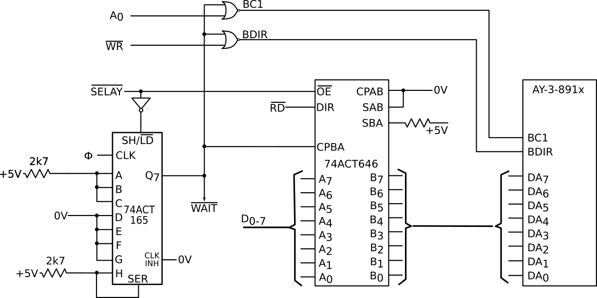
\$\small\overline{SELAY}\$ is the active low select signal for an I/O cycle to the PSG, as discussed previously.
There's a big caveat in that I haven't built this so there might be the odd mistake in the diagram but I think that it should work OK. (remember, always, however, the difference between theory and practice

)
The timing is as follows (\$\Theta = 8MHz\$)
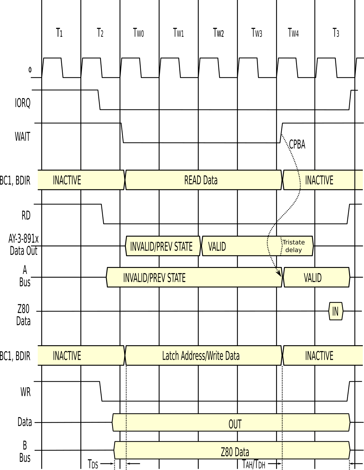
All of the 3-8912 timing requirements are met with the exception of the data setup time - if we accept that the negative numbers in the Z80 timing information mean that the data is not guaranteed to be stable when \$\small\overline{WR}\$ falls then an 8MHz Z80 might not get it's act together until 10ns before the rising edge of the clock at the end of T2 (TdCr(WRf)-TdD(WRf)IO - 60 - -55ns = 115ns), add in the propagation delay through the 74ACT646 and the data is not guaranteed to be stable at the PSG until pretty much the rising edge of the clock at the end of T2. That edge clocks the data to drive \$\small\overline{WAIT}\$ low and start the bus cycle on the 3-8912, there is an additional delay through the NOR gates before BC1 & BDIR change state so there should be a guaranteed 20ns or so of data set-up time - not officially enough but better than -55ns.
The wait sates can be extended by changing which of the 74ls165 inputs are tied high and which tied low. Up to 7 wait states can be generated to this should be good up to a 14MHz clock for the Z80. Beyond that the wait state generator, at least, will need a rethink.
Enjoy.


