Hi everyone,
I recently had a dead Keyence LJ-V7060 head (unit was not recognized by the controller). Since these units are usually "black boxes" in the industry, I decided to perform a destructive teardown to see the engineering behind a 64kHz profilometer.
I use several of these systems in my own builds, so I was particularly interested in the optical path and how they handle thermal drift.
Exterior and Housing The LJ-V7060 is built like a tank. Heavy-duty cast aluminum housing, held together by high-torque Torx screws. You can see the 405nm (Blue/Violet) optics and the typical industrial ruggedness.


Internal Layout After opening it up, the internal structure reveals a main logic board in the top section and a separate opto-mechanical base plate. The isolation between the processing electronics and the optical path is quite clear.


The Laser Module & Thermal Management The laser module is fixed with a white, flexible RTV-like material. It seems Keyence chose this for vibration damping and to allow for thermal expansion without losing line alignment. The empty shell shows machined surfaces and thermal pads designed to dump heat from the FPGA/DSP directly into the housing.


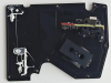
CMOS Sensor side In contrast to the laser module, the CMOS sensor module is potted with a hard, resin-like material (likely epoxy) to ensure absolute rigidity for the triangulation geometry.


If you’re curious about the hardware, the integration, or just general nature of this hardware, feel free to ask. I’ll do my best to answer.
Enjoy the hardware porn!


 Home
Home Help
Help Search
 Login
Login Register


