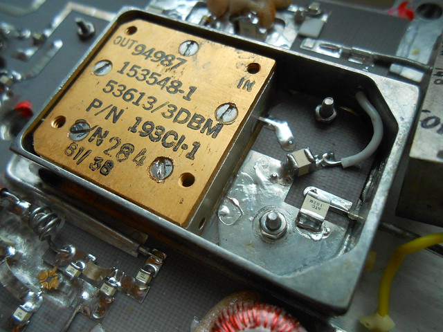
Cubic Defense Systems mystery board (large)Here's one of a couple modules
I got from here that were being sold for parts << $20. "94987", which pops up everywhere, is the CAGE code for "Cubic Defense Systems", for what it's worth.


Because signal paths are nice and easy to follow on single-layer RF boards, we can see that a signal comes in at one end, passing through one of the bottom-side-metal-can amplifiers(?) and then a circulator...
...passes through a couple discrete-transistor amplification stages, with tombstone'd SMT power filter caps...


...and then goes to a directional coupler, where some of the signal gets picked off:

A second signal input goes through an amplifier of its own, with some big blobs of foam to hold inductors in place...
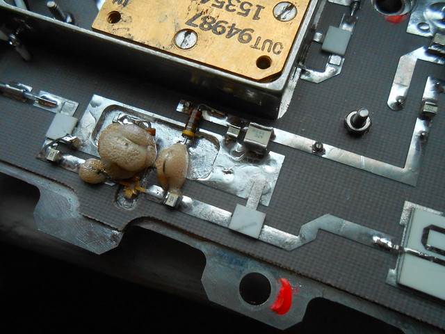
...and then goes to a coupler of its own:
By the way, those small metal boxes on each input & output are confirmed to be filters, with very "ship-in-a-bottle" construction. This one looks like maybe a bandpass:

Both output signals sampled from those directional couplers then travel to a middle section, where they're mixed together in the "CF049" module, and then boosted by the 2nd bottom-side-metal-can amplifier before being sent out over yet another coax. Opening it the "CF049" module got messy, so no good photos there, but it had 3 tiny magnetics and a tiny diode bridge inside: a double-balanced diode mixer.


Overall, the block diagram looks like this:

The signal flow vaguely suggests that one of the signal paths is a transmitted RF signal, and the other is an LO signal, and the "monitor" circuitry in the middle is downconverting the RF-Tx signal to an IF to make sure that the output amplitudes of both RF & IF are in a normal range etc. etc.
I'm not sure why the top signal path has the most-heavily-heatsinked amplifier (the metal-can one) coming
first in the signal chain, and followed by a circulator. It might be performing some non-linear function, like a frequency multiplier?
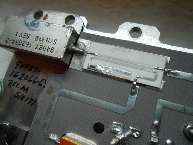
Let's look inside both those metal cans to see what's happening there, because I couldn't find anything useful with the part numbers, and also because finding miniature accidental-hybrid-artworks inside mystery boxes is fun. As a quick side note, you can see some creative power routing on the bottom of the heatsink here, with grooves milled into it where discrete wires are run for distributing the supply voltage.

Here's the metal can that boosts the mixed output:


It's a pretty standard-looking RF amplifier in most ways, a common-emitter (Q1) with a large spiral coil that forms a tapped auto-transformer for stepping down the voltage from the transistor's collector. Q3 and associated components form a biasing circuit that attempts to regulate the DC collector current of Q1: R5 works as a current sense resistor, and so when Q1's collector current is too low, the voltage on Q3's emitter increases. This increases Q3's Vbe (because its base voltage is fixed by the R6/R7 voltage divider) and increases Q3's collector current, which increases the base(/gate?) bias on Q1.
The strange part though is Q2. I have no idea what this is doing here. It has a larger die than Q1, and the patterning I can see on the surface makes it look more like a high-frequency transistor, rather than a very "normal" BJT like Q3. The connections don't make sense, unless it breaks the standard pinout of "bottom of die = collector/drain". If it really does have the base(/gate?) connection where I showed it, then it seems like it would operate off of a kind of "current sense" for Q1. Any insights here would be appreciated.
Let's take a look at these nice spiral inductors, and resistive traces in the biasing circuitry:


Now, here's the metal can the precedes the circulator:


The biasing is much simpler here because it appears to be a common-base amplifier, with Q1's DC setpoint determined only by the R2/R3 voltage divider, and R1 (ignoring Q1's Vbe, that is). The DC-blocking capacitors here are little vertical single-layer flat plates, rather than the big SMT multi-layer ceramic caps in the previous metal can, which suggests that the operating frequencies here are higher. The step-down auto-transformer/tapped-inductor L1 here makes sense, as a common-base amplifier has a very low input impedance equal to the incremental resistance of Q1's Vbe: so here you get the best performance by stepping down the 50Ω(?) input to match the much lower transistor impedance.
So, I'm still not sure why the whole board's signal chain is laid out the way it is. This device isn't a mixer or anything else obviously non-linear, and it seems to be used as an amplifier rather than a frequency multiplier: even if Q1 was driven heavily to the point where it saturated each cycle and produced a lot of harmonics, you'd expect to see a lot of filtering following it, to select only the desired harmonic and suppress all the others. I have to admit that I'm also not sure what the benefits are of a common-base vs. common-emitter amplifier are in an RF context where impedances are fairly constant; the tradeoffs are much more obvious at low frequencies, but I'm not a full-time RF guy. Might have something to do with noise figure, or specific types of transistors available?
There's nothing else particularly noteworthy in this metal can, except that the inductors are rectangular(!!!) instead of circular:

Fuck, I love microscopes.
You can also see some trimming (or parameter selection?) of one of the resistors, with wirebonds selectively bypassing sections of it to tune the resistance.
Anyways, hope you enjoyed the close-ups.


