OldSchoolTechCorner, I can't wait to see what's inside your unit.
While waiting for parts, I now took a close look on analog boards.
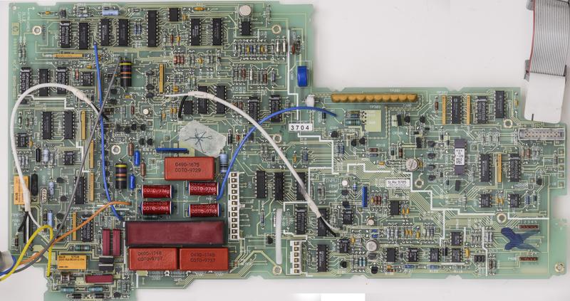
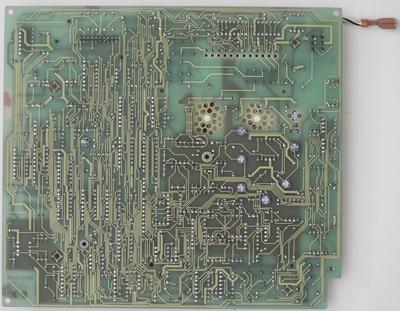
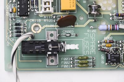
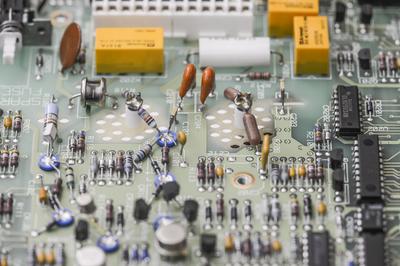
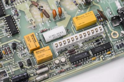
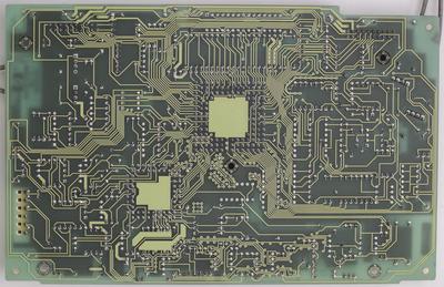
A1 boardThis board also have mark "X" around reference header, also paper tape sticker "X" in center of board near RP7 resistor network. Visual inspection shows ugly soldering and flux around parts U300, U305, U301, RP300, U304, U306, RP301, U303, RP302, RP303, R308, R307, R310, RP200 and around all relays (K1, K2, K3, K4, K5, K6, K7, K9, K200, K201, K202, K203, K204). Relays have datecodes from 1997, while rest of the board IC's dated 1995-1996. Previous owner tried to fix board by replacing relays?
Looking not good, if you ask me. Those COTO relays, HP resistor network RP300 are unobtanium. U300 OPA111BM is rather expensive too, 50 USD a pop on Digikey.
I claim world-record highest resolution photos of 3458A stuff ever,

That's what happening, when photo-nut comes to volt-nuttery...
98MP, front side.
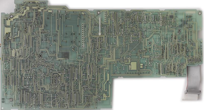
96MP back side.
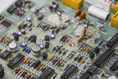
Soldering "job"
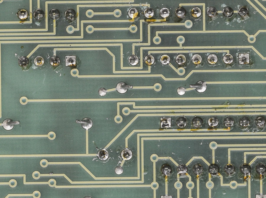
Some people just don't know what they are doing in terms of repairs

. That's why buying gear "after repair" sucks, often it's worse as than getting unknown, never serviced gear.
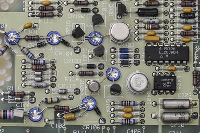
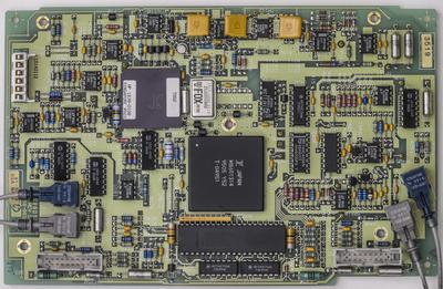
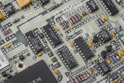
Rest of boards seem to be OK looking
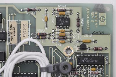
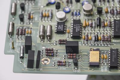
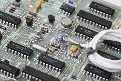
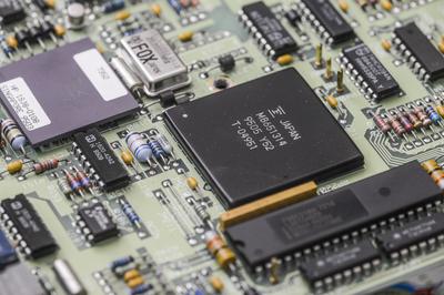
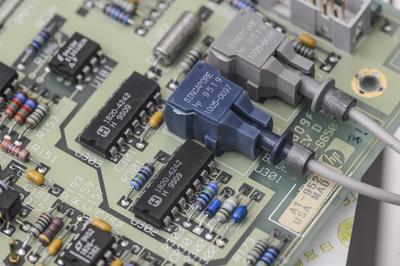
A2 PCBA:
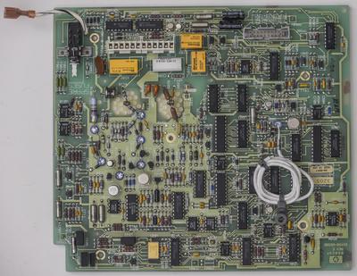
Rest of details on this board:
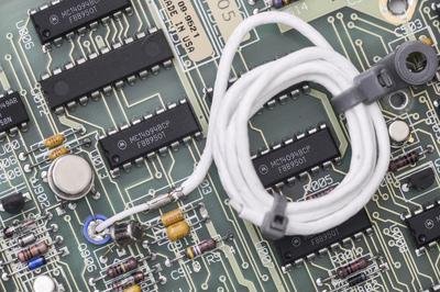
That piece of wire looks interesting, funky low-capacitance capacitor, perhaps?
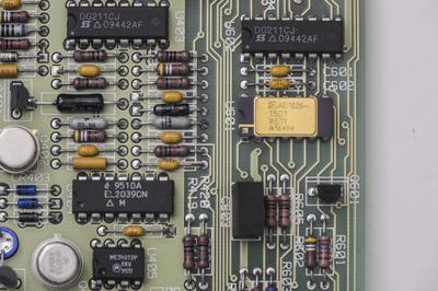

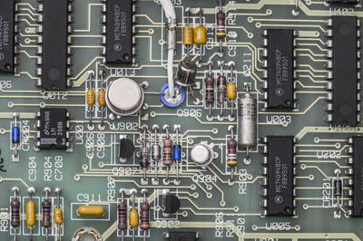

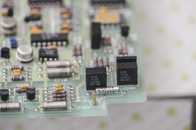
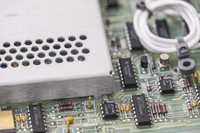
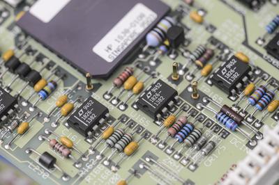
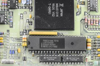
A3 ADC PCBA:
Rest of details on this board:

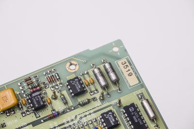
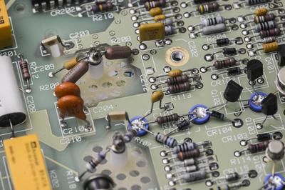
Also another thing I noticed, guard traces are covered with soldermask. Isn't that defeat purpose of guard trace? Or it was an issue to manufacture with open copper in 90's?


