Author Topic: Transistors - die pictures  (Read 192218 times)

0 Members and 3 Guests are viewing this topic.

Offline mister_rf

  • Contributor
  • Posts: 33
  • Country: ro
Re: Transistors - die pictures
« Reply #675 on: January 18, 2023, 10:15:26 pm »
ITT Semiconductors 2N2222A


The following users thanked this post: SeanB, exe, RoGeorge

Offline mister_rf

  • Contributor
  • Posts: 33
  • Country: ro
Re: Transistors - die pictures
« Reply #676 on: January 18, 2023, 10:18:49 pm »
National Semiconductor J 2N2222A


The following users thanked this post: SeanB, exe, RoGeorge

Offline mister_rf

  • Contributor
  • Posts: 33
  • Country: ro
Re: Transistors - die pictures
« Reply #677 on: January 18, 2023, 10:22:33 pm »
IPRS BANEASA – Bucharest, Romania -  2N2222


The following users thanked this post: SeanB, exe, RoGeorge

Offline exe

  • Supporter
  • ****
  • Posts: 2564
  • Country: nl
  • self-educated hobbyist
Re: Transistors - die pictures
« Reply #678 on: January 19, 2023, 09:27:46 pm »
So... Which 2N2222 is the best? :)
 

Online T3sl4co1l

  • Super Contributor
  • ***
  • Posts: 21707
  • Country: us
  • Expert, Analog Electronics, PCB Layout, EMC
    • Seven Transistor Labs
Re: Transistors - die pictures
« Reply #679 on: January 19, 2023, 10:12:35 pm »
2N4401 ;D

Tim
Seven Transistor Labs, LLC
Electronic design, from concept to prototype.
Bringing a project to life?  Send me a message!
 

Offline BrianHG

  • Super Contributor
  • ***
  • Posts: 7749
  • Country: ca
Re: Transistors - die pictures
« Reply #680 on: January 19, 2023, 10:31:51 pm »
So... Which 2N2222 is the best? :)
Well, the Motorola one is a mutant.
The CRP INDUSTRIES one combs your hair.
The ITT Semiconductors one needs help.
The National Semiconductor one is intelligent.
The IPRS BANEASA one stealthily flies.
« Last Edit: January 19, 2023, 10:35:14 pm by BrianHG »
 

Offline mister_rf

  • Contributor
  • Posts: 33
  • Country: ro
Re: Transistors - die pictures
« Reply #681 on: January 19, 2023, 10:33:33 pm »
So... Which 2N2222 is the best? :)

Perhaps the question should be formulated as follows: What’s the practical difference between these transistors?  8)
It's interesting that the idea came to me when I've found 4 x 2N2222 transistors on the same board, but each has been manufactured by a different company.
 
The following users thanked this post: MegaVolt

Offline David Hess

  • Super Contributor
  • ***
  • Posts: 16627
  • Country: us
  • DavidH
Re: Transistors - die pictures
« Reply #682 on: January 20, 2023, 01:41:26 pm »
2N4401 ;D

I concur.

So... Which 2N2222 is the best? :)

Well, the Motorola one is a mutant.

The Motorola one shows the structure of the original 2N2222 which gave it its performance.  The others rely on better processes.

 
The following users thanked this post: SeanB

Offline BrianHG

  • Super Contributor
  • ***
  • Posts: 7749
  • Country: ca
Re: Transistors - die pictures
« Reply #683 on: January 20, 2023, 02:22:35 pm »
2N4401 ;D

I concur.

So... Which 2N2222 is the best? :)

Well, the Motorola one is a mutant.

The Motorola one shows the structure of the original 2N2222 which gave it its performance.  The others rely on better processes.
The 'Mutant' stood for 'Marvel's X-Men' from their comics / movie cinematic universe.
 

Offline David Hess

  • Super Contributor
  • ***
  • Posts: 16627
  • Country: us
  • DavidH
Re: Transistors - die pictures
« Reply #684 on: January 20, 2023, 03:16:42 pm »
Quote
So... Which 2N2222 is the best? :)

Well, the Motorola one is a mutant.

The Motorola one shows the structure of the original 2N2222 which gave it its performance.  The others rely on better processes.

The 'Mutant' stood for 'Marvel's X-Men' from their comics / movie cinematic universe.

The discussion about what made the 2N2222 unique at the time starts here:

http://www.semiconductormuseum.com/Transistors/Motorola/Haenichen/Haenichen_Page7.htm
 
The following users thanked this post: exe

Offline NoopyTopic starter

  • Super Contributor
  • ***
  • Posts: 1742
  • Country: de
    • Richis-Lab
Re: Transistors - die pictures
« Reply #685 on: February 07, 2023, 06:47:00 pm »


The KCZ58 is a dual transistor built by Tesla. The maximum Vce0 is 30V, the maximum collector current is 100mA, and the power dissipation must remain below 450mW. The current gain factors range from 100 to 500, with the ratio of the two transistors given as 0,9 - 1,11. Judging from the specifications, the KCZ59 was a lower grade of the same product. The range of possible current gain factors is slightly larger at 50 - 500 and the ratio of the two transistors may range from 0,8 to 1,25.

RG probably stands for a production in July 1978. The number 1 cannot be assigned.  :-//


There are two individual transistors in the package. The collector potentials are supplied via metal sheets, which in addition serve as a support for the transistors.


Each transistor has an edge length of 0,59mm. It is the known structure, where a round emitter is located in a round base, which has a bulge as contact area. The square with the underlying cross-shaped structure was certainly used to check the alignment of the masks.

The right transistor seems damaged in the left area of the emitter, but works completely normally. It is probably just an impurity.


The base-emitter junction breaks down at -7,5V and shows the familiar glow of an avalanche breakdown. The current increases from top to bottom: 10mA, 50mA, 100mA. The uniform glow suggests that the transistor is not damaged and the artifact is just a minor contamination.


https://www.richis-lab.de/BipolarA20.htm

 :-/O
 
The following users thanked this post: SeanB, RoGeorge

Online RoGeorge

  • Super Contributor
  • ***
  • Posts: 6217
  • Country: ro
Re: Transistors - die pictures
« Reply #686 on: February 07, 2023, 07:41:14 pm »
A reversed BE can be used as a noise generator.  I wonder how much noise correlation would be if each transistor in such a pair would be used as an independent noise generator.  ???

Offline NoopyTopic starter

  • Super Contributor
  • ***
  • Posts: 1742
  • Country: de
    • Richis-Lab
Re: Transistors - die pictures
« Reply #687 on: February 07, 2023, 07:51:17 pm »
A reversed BE can be used as a noise generator.  I wonder how much noise correlation would be if each transistor in such a pair would be used as an independent noise generator.  ???

Ignoring external influences I would assume there is no correlation since it is a stochastic process. But I don´t really know...  :-//

Offline NoopyTopic starter

  • Super Contributor
  • ***
  • Posts: 1742
  • Country: de
    • Richis-Lab
Re: Transistors - die pictures
« Reply #688 on: February 12, 2023, 09:47:24 pm »


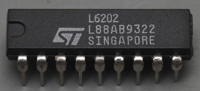
L6202 a famous H-bridge built by STMicroelectronics (SGS-Thomson to be honest). It´s more than a transistor but I have put it to the "special transistors".

In this Powerdip18 package, the device can carry up to 1,5Arms. Alternatively, a SO20 package is offered, but it allows just 1Arms. For higher power, a Multiwatt11 and a PowerSO20 package make it possible to conduct up to 4Arms. The peak current may increase up to 5A. The SO20 package is limited to 2A in this regard. The typical resistance of the switches is 0,3Ω. The maximum permissible supply voltage is 48V. The typical clock frequency is given in the datasheet as 30kHz, 100kHz is specified as the maximum. The L6202 ensures with a dead time of 100ns that never both switches are conductive at the same time.


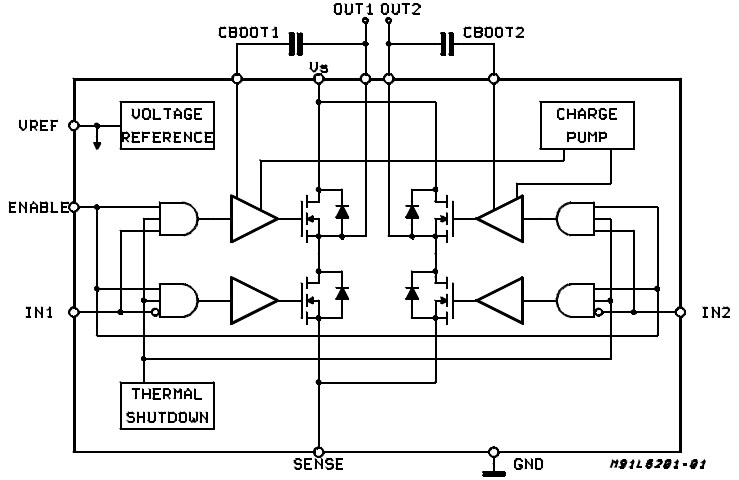
The block diagram in the datasheet shows the construction of the L6202. The H-bridge is built with four NMOS transistors. The negative potential of the H-bridge is isolated from the ground potential, so that a shunt for current measurement can be looped in.

According to the datasheet, the NMOS transistors are switched with a gate-source voltage of 10V. However, this also means that a separate supply voltage must be generated for the two highside transistors. This voltage can be obtained from two different sources. A charge pump ensures that the highside transistors can be switched on from a longer inactive phase. If switching gets faster, the charge pump would probably not be powerful enough. For this, bootstrap capacitors must be connected to the L6202, which lift the necessary larger amounts of charge to the high potential when the H-bridge is switched. According to the datasheet, the capacitance should be at least ten times as large as the input capacitance of the transistor, which is 1nF.

Four gates can be used to switch the two sides of the H-bridge. An enable input allows to switch off all transistors. An overtemperature protection switches the H-bridge off at temperatures above 150°C. The L6202 contains a 13,5V reference voltage source which must be stabilized externally with at least 220nF. One may then load the reference with up to 2mA.


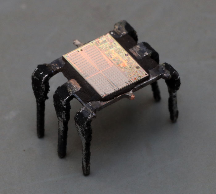
The six pins in the middle of the package are connected to ground. It can be seen that these pins are combined into a carrier on which the die is placed. This improves the power dissipation. Accordingly, the datasheet recommends connecting a large copper area to the six pins in the middle of the package.


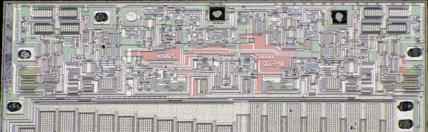
The dimensions of the die are 5,1mm x 4,0mm. According to the datasheet, the device was manufactured with a BCD process. This allows the control circuit to be built with the benefits of bipolar and CMOS transistors, while high-performance DMOS transistors are used in the H-bridge. There are indications that the L6202 was the first device to be manufactured with a BCD process at STMicroelectronics, SGS-Thomson respectively.


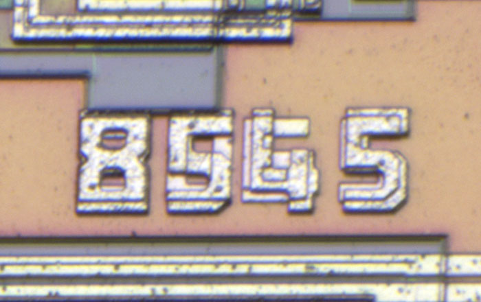
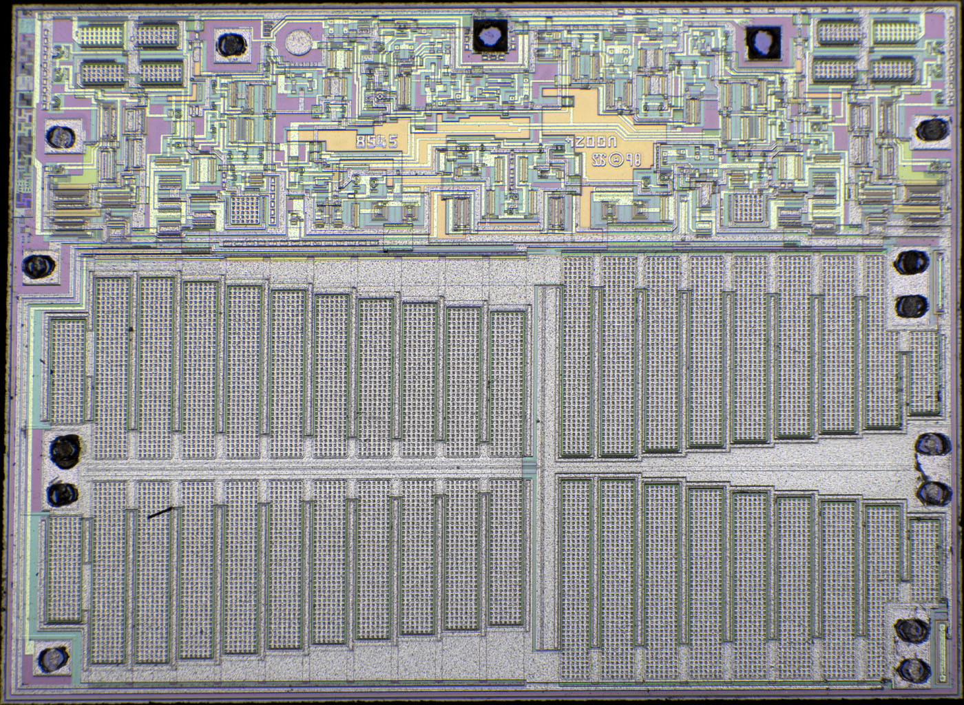
Somewhat to the left of center, several numbers are shown on top of each other. It seems that there are two metal layers used here. In the circuit itself, however, only one metal layer can be seen. The lower number is 8065, the upper 8545. The meaning remains unclear.


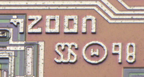
To the right of the center, the logo of SGS Thomson and the year 1986 are shown. The string U0024 could be an internal project designation.


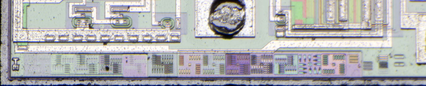
On the left edge, there are some structures that allow to monitor the imaging performance of the process. The 13 squares could indicate a mask set with 13 masks.


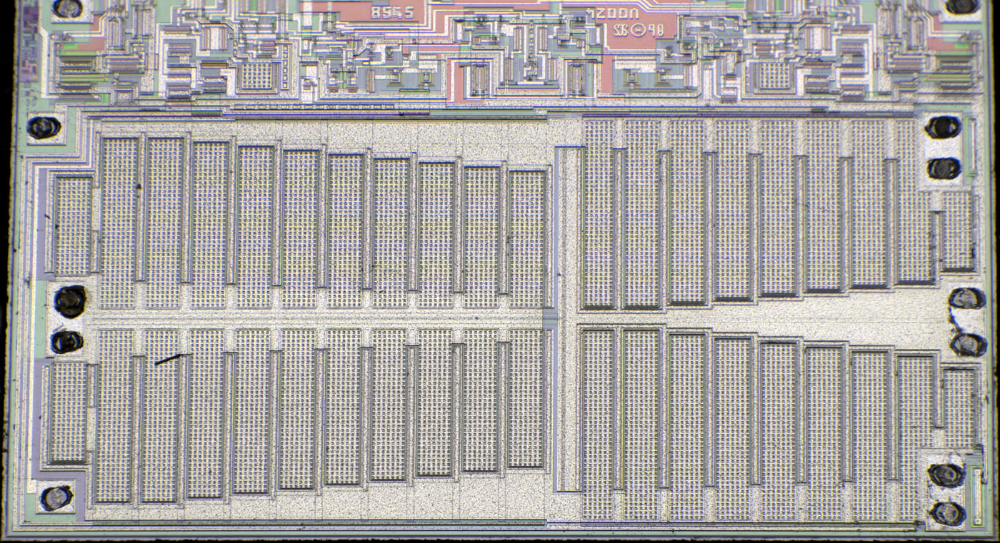
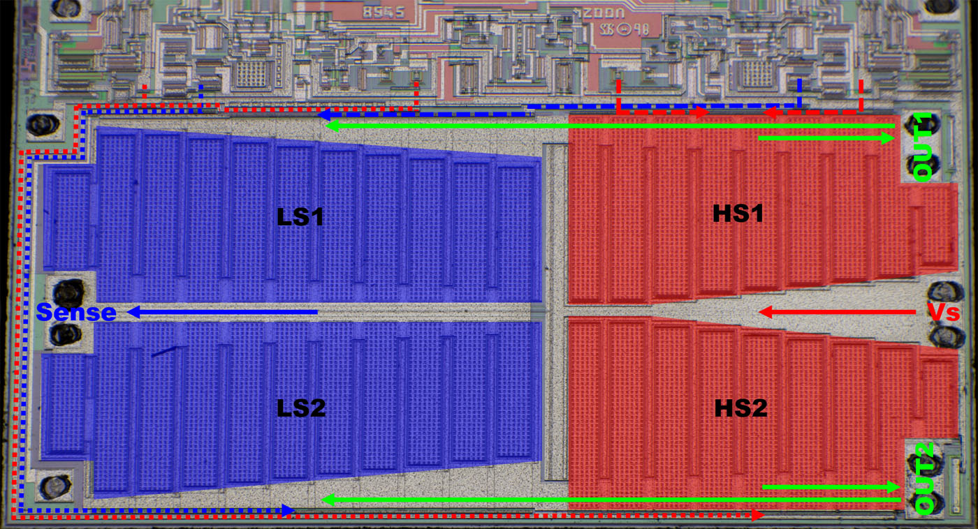
The interconnection of the four power transistors is clearly visible. The width of the lines is adapted to the respective local current. At first glance, the lowside transistors appear somewhat larger than the highside transistors. However, the highside transistors are slightly wider, resulting in approximately equal areas, as would be expected with four NMOS transistors. The gate potentials are fed from the top and from the bottom.


The control circuit is relatively clear. It is easy to see that each highside transistor is supplied from two areas. The charge pumps seem to be located in the center. Two very large, reddish areas are integrated there, which certainly represent the associated capacitances.

On the left and right edges, the bootstrap bondpads are placed respectively. In these areas is another control for the gate electrodes. Four larger elements are integrated in each of the corners. It could be that these are transistors that limit the gate-source voltage. After all, this voltage could approach the maximum permissible supply voltage of 48V.


https://www.richis-lab.de/FET30.htm

 :-/O
« Last Edit: February 12, 2023, 10:37:13 pm by Noopy »
 
The following users thanked this post: RoGeorge, karpouzi9

Offline NoopyTopic starter

  • Super Contributor
  • ***
  • Posts: 1742
  • Country: de
    • Richis-Lab
Re: Transistors - die pictures
« Reply #689 on: February 15, 2023, 04:12:09 am »
these die photos are phenomenal! nice work Noopy!

Thank you!
I still have plenty pictures on my hard drive and a lot of parts in stock.  8)

Offline NoopyTopic starter

  • Super Contributor
  • ***
  • Posts: 1742
  • Country: de
    • Richis-Lab
Re: Transistors - die pictures
« Reply #690 on: March 04, 2023, 02:52:17 pm »


The MJE3055 is an alternative to the 2N3055 (https://www.richis-lab.de/2N3055.htm). Here, however, the maximum permissible collector current is not 15A, but only 10A. The TO127 package is slightly larger than a TO220 package and thus allows a power dissipation of up to 90W. The MJE3055 is thus slightly less powerful than the 2N3055 in the TO3 package. In the alternative TO220 package, the MJE3055 allows just 75W. Maximum Vce is 60V, cutoff frequency is 2MHz.


Inside the package there is a relatively thick carrier. A silicone-like potting protects the die and bondwires.


The potting is easy to remove.


The dimensions of the die is 3,2mm x 2,8mm. It seems to be the same transistor that Motorola used in the 2N3055I (https://www.richis-lab.de/2N3055_10.htm).


Typical for a MESA transistor, the edges are etched down, resulting in clean outer edges at the base-collector interface. The etching process has left an interesting surface texture.


Emitter and base form the typical structures of a power transistor. For contacting the surfaces, there are vias in the protective passivation layer, the edges of which become visible in the surface of the metal layer.


https://www.richis-lab.de/BipolarA21.htm

 :-/O
 
The following users thanked this post: SeanB, RoGeorge, floobydust

Offline NoopyTopic starter

  • Super Contributor
  • ***
  • Posts: 1742
  • Country: de
    • Richis-Lab
Re: Transistors - die pictures
« Reply #691 on: March 06, 2023, 06:31:28 pm »


Now the MJE2955, the complementary PNP transistor to the MJE3055. It has exactly the same specifications.


The mechanical construction is the same as in the MJE3055. However, much more solder seems to have been used to fix the die. The solder has spread over the carrier. A silicone-like potting was used here too.


The die is constructed in the same way as the die of the MJE3055. However, the MJE2955 being a PNP transistor is significantly larger. The dimensions are 3,6mm x 3,1mm, compared to the 3,2mm x 2,8mm of the MJE3055.


Unlike the MJE3055 the surface of the etched-down edges is very smooth.


The metal layer is slightly offset downwards compared to the other structures.


https://www.richis-lab.de/BipolarA22.htm

 :-/O
 
The following users thanked this post: SeanB, RoGeorge, floobydust

Offline NoopyTopic starter

  • Super Contributor
  • ***
  • Posts: 1742
  • Country: de
    • Richis-Lab
Re: Transistors - die pictures
« Reply #692 on: March 31, 2023, 08:17:58 pm »


The 2N6543 is a switching transistor which can isolate up to 400V. A collector current of 5A is constantly permissible, up to 10A is possible for a short time (1ms/10%). The base path is specified with the same current carrying capacity, so in addition to the collector current, the datasheet specifies a maximum emitter current, which can be correspondingly twice as high (10A/20A). The cut-off frequency is between 6MHz and 28MHz. At 25°C 100W can be dissipated via the housing. The characteristic values are taken from a RCA datasheet. The 2N6543 shown here was manufactured in 1980 by the American company TRW.


The RCA datasheet contains an SOA diagram. It clearly shows how optimization to best switching performance affects the behavior in the linear area. Just in a small range the area is limited by the maximum power dissipation. A much stronger limitation results from the very early onset of the second breakdown.


The emitter is connected to the die via two bondwires.


Here, the bondwires have been welded to the side of the connection pins.


The die is located on a base, which is equipped with a trench. Excess solder collects in this trench when the die is soldered on the base.


The edge length of the die is 5,1mm. Unusual is the use of two emitter areas. The lower and upper comb structures each represent an isolated emitter surface. The imprints of test needles can be seen on the metal surfaces.


To isolate the high voltage, there is a structure in the outer area which controls the potential distribution. Otherwise, the electric field would be too inhomogeneous and flashovers would occur at the edge of the transistor.

Between base and emitter more structures are visible than one would expect. On closer inspection, the grey areas seem to be contact areas, which are wider than the metal areas. Brown would then be the base doping and purple the emitter doping. This would also match the colors of the potential distribution.


At a voltage of -10V, the base-emitter junction breaks down and the typical glow effect of an avalanche breakdown is seen (current levels: 20mA, 50mA, 100mA, 200mA, 500mA, 1A, 2A).


https://www.richis-lab.de/BipolarA23.htm

 :-/O
 
The following users thanked this post: SeanB, RoGeorge, floobydust

Online T3sl4co1l

  • Super Contributor
  • ***
  • Posts: 21707
  • Country: us
  • Expert, Analog Electronics, PCB Layout, EMC
    • Seven Transistor Labs
Re: Transistors - die pictures
« Reply #693 on: March 31, 2023, 11:20:59 pm »
Nice one.

Excuse this bit of pareidolia: ;D

Tim
Seven Transistor Labs, LLC
Electronic design, from concept to prototype.
Bringing a project to life?  Send me a message!
 

Offline NoopyTopic starter

  • Super Contributor
  • ***
  • Posts: 1742
  • Country: de
    • Richis-Lab
Re: Transistors - die pictures
« Reply #694 on: April 01, 2023, 03:07:53 am »
Yeah, sometimes they talk to me...  ;D
 
The following users thanked this post: exe, RoGeorge

Offline NoopyTopic starter

  • Super Contributor
  • ***
  • Posts: 1742
  • Country: de
    • Richis-Lab
Re: Transistors - die pictures
« Reply #695 on: April 03, 2023, 03:11:11 am »


The NDUL09N150C from ON Semiconductor is a power MOSFET that can block up to 1500V. In order to provide sufficient isolation distances, the TO-3PF package has an additional plastic collar on the drain pin. A metallic cooling fin is missing. This worsens the thermal resistance (1,6°C/W), but makes assembly easier because no additional insulation layer has to be added. With a housing temperature of 25°C, the MOSFET can dissipate up to 78W. The typical Rdson is 2,2Ω. The datasheet states two different current carrying capacities. The transistor itself would allow 9A permanently, but the package limits this value to 6A. At 6A, there is already more power loss than can be sensibly dissipated via the housing. Up to 18A is permissible for a short time.


The die has an edge length of 8mm. The thickness is approximately 0,25mm. The source bonding area is in the centre. The connection for the gate potential is placed on the left edge. Only one bondwire was used for the source connection, but with a much thicker cross-section than for the gate connection.


The die is covered with a protective layer, probably polyimide. Next to the source connector is a window that appears to be for testing purposes.


The familiar round structures for potential control are integrated at the edge of the die so that no flashovers occur at up to 1500V.


The gate potential is conducted over a frame, around the perimeter of the active area, and makes contact at the upper and lower edges with deeper lying lines leading into the active area.

The metal surface that conducts the drain potential is connected to the underlying trench MOSFET structures via long vertical openings.


The layers are difficult to remove. Here, however, you can see that the gate potential is led into the MOSFET via the yellowish surfaces. From the lateral contacts, the surface has already been heavily attacked.

The drain potential contacts the MOSFET not only via the vertical strips, but also at the edges. This measure is presumably intended to ensure that the potential around the active area is always the same at all points and that there is no local excess in the electric field.


https://www.richis-lab.de/FET31.htm

 :-/O
 
The following users thanked this post: SeanB, RoGeorge

Offline NoopyTopic starter

  • Super Contributor
  • ***
  • Posts: 1742
  • Country: de
    • Richis-Lab
Re: Transistors - die pictures
« Reply #696 on: April 23, 2023, 07:50:57 pm »


The TDE1647 is a relay and lamp driver from Thomson Semiconducteurs. It blocks up to 50V and conducts up to 1A. The value to which the short-circuit current is limited can be set via an external shunt. The device also contains an overtemperature cutoff.


The datasheet contains a block diagram showing how the TDE1647 works. The two inputs control a differential amplifier that controls a power transistor at the output. Depending on the voltage drop across the external shunt, another transistor shunts the base current of the power transistor, limiting the output current. The overtemperature protection can sink the base current too. The square with the G possibly stands for the ground loss protection circuit that the TDE1747 includes. The TDE1747 shares a datasheet with the TDE1647.


The datasheet contains a complete circuit diagram of the TDE1647 / TDE1747 too. At the input is a classic differential amplifier (yellow). The current source of the differential amplifier belongs to a bias network (blue), which is based on a reference current source (cyan).

The output signal of the differential amplifier passes through two amplifier stages (pink). The actual amplifier stage consists of the Darlington pair Q6/Q9. The transistor Q5 diverts the base current of this Darlington pair when it is activated.

The grey circuit part represents the overtemperature protection. A constant potential is applied to R2. If the temperature increases, the base-emitter voltage of Q28 drops and a current flows through R10. The current mirror Q17 conducts a proportional current through D3 to Q28 and thus realises a hysteresis. At the same time, transistor Q29 becomes active, which diverts the current from current source Q15 without which the output stage switches off.

The control signal of the output transistor passes through a surprisingly complex circuit (purple). This appears to be the ground loss protection circuit of the TDE1747. If a current flows through the Darlington transistors Q6/Q9, it also flows through Q23 and activates the output stage. In the event of a ground loss, the voltage drop across this circuit is very low. Then the current path via Q25 and Q22 dominates and the current of the current source Q15 is diverted so that the output stage remains inactive.

The output stage is controlled via transistor Q18 (dark red). The output stage (red) consists of a Sziklai pair. (There is a point missing in the circuit diagram.) In the overcurrent protection (green), Q24 can dissipate the base current of the output stage.


The housing has six pins. The pins carrying power are grouped on the right, while the control and the ground potential are supplied on the left.


The dimensions of the die are 4,2mm x 2,9mm. The individual elements are clearly visible.

The output stage transistor consists of three areas. The widths of the lines are adapted to the local current strengths. Each area has a resistor on the emitter side, which guarantees an even current distribution. Where each emitter strip is contacted, the contour of a taper is visible in the metal layer, which represents an emitter resistor for the individual transistor. It is interesting to note that in the uppermost area, the emitter strip on the far left has been omitted.

At the upper edge there is an elongated structure. This is the driver transistor, which as a PNP transistor must be relatively large.


The die already bears an ST logo. Next to it, a symbol has been integrated that is reminiscent of a lighthouse. Perhaps this is an allusion to its function as a lamp driver.


The revisions of eight masks are shown at the bottom edge. According to this, all masks were revised once and one twice.

The numbers 1747 show that this design can also be used for the TDE1747. Analysing the circuit, it can be seen that the circuit part which probably represents the ground loss protection circuit is present and active here. This means that a TDE1747 has actually been built into this TDE1647.


P160 could be an internal project designation or a designation for the manufacturing process used.


https://www.richis-lab.de/BipolarA24.htm

 :-/O
 
The following users thanked this post: SeanB, Miyuki, ch_scr, MegaVolt, karpouzi9

Offline NoopyTopic starter

  • Super Contributor
  • ***
  • Posts: 1742
  • Country: de
    • Richis-Lab
Re: Transistors - die pictures
« Reply #697 on: April 30, 2023, 07:33:16 pm »
Here comes an update for the TDE1647:


I got the hint that the logo right of the ST logo probably show the Eifel tower. 1937 a company that later became Thomson Semiconducteurs performed the first radio transmission from the Eifel tower.


If you analyze the circuit on the die, you will find a few minor differences to the schematic.


If you redraw the schematic accordingly, you get the following picture.

The resistor R2 between the resistors R13 and R14 is missing on the die. Likewise, resistor R7 is missing in the supply line of Q23 and Q18. Instead, there is a resistor in the supply line to Q17, which is missing in the schematic. Sometimes such resistors are just undercrossings and their value is irrelevant. Here, however, it seems to be an intentional resistor.

Q6 is not supplied by Q13 in the real circuit, but by Q15. There is a diode between Q15 and Q6.

Q24, which is the overcurrent protection, owns a base resistor on the die. There is also a surprisingly large diode in the collector path. This was probably used to adjust the tripping voltage of the overcurrent protection.


https://www.richis-lab.de/BipolarA24.htm#Update
 
The following users thanked this post: SeanB, RoGeorge

Offline NoopyTopic starter

  • Super Contributor
  • ***
  • Posts: 1742
  • Country: de
    • Richis-Lab
Re: Transistors - die pictures
« Reply #698 on: May 01, 2023, 09:24:18 am »


The TDE1737 is a relay and lamp driver like the TDE1647. While the TDE1647 contains a highside output stage, the TDE1737 has a lowside output stage. The reverse voltage is up to 50V, the current may rise up to 1A.


Pretty similar to the TDE1647.


The differential amplifier at the input (yellow) is similar to the one in the TDE1647. However, the common current source is missing here. The current through the branches is adjusted just via the transistors Q3/Q4. The bias setting (blue) and reference current sink (cyan) look the same like in the TDE1647.

The output of the differential amplifier passes two amplifier stages (pink). The second amplifier stage is reminiscent of a Darlington transistor. However, Q6 is connected as a diode. Either one wanted to provide the possibility to build up a Darlington transistor or Q6 ensures that Q9 switches off more slowly and the output stage switches on with a minimal delay. In addition, it could of course be a remnant of the TDE1647 circuit, which is quite similar to the TDE1737.

As long as the transistor Q9 is inactive, the current of the current source Q15 controls the output stage, which consists of a Darlington transistor (red). As overcurrent protection, transistor Q24 (green) diverts the base current of the output stage if too much voltage drops across the external shunt.

The overtemperature protection of the TDE1737 (grey) is based on the reference voltage of the reference current sink (cyan). If the temperature rises, the base-emitter voltage of Q18 drops and a current flows through Q18, Q21 and Q17. The current mirror Q17 then controls Q16 and diverts the base current of the output stage through it.

The remaining elements (purple) appear to perform a similar function to the ground loss protection circuit in the TDE1647. Ground loss is less critical in a lowside driver. However, the circuit could protect the TDE1737 against supply voltages that are too low to guarantee a proper functionality. Only when the voltage between Vcc and GND is high enough for D2 to conduct, Q23 diverts current from current source Q15, thus deactivating transistor Q22, which otherwise, like transistor Q16, keeps the output stage inactive.


The dimensions of the die are 2,1mm x 1,4mm. On the lower edge, a relatively large logo refers to ST Microelectronics.


On the upper edge there is a year which is difficult to identify. It looks like 1985.


In the lower left corner, the characters 1737.C are shown in the metal layer. The C could stand for a third revision of the design.


In the upper left corner the mask revisions are shown. Two masks are difficult to see, but as with the TDE1647, there are seven masks in total.


X057 could be an internal project designation.


A closer analysis of the dies reveals some minor differences to the schematic. It is also noticeable that the design is very similar to the TDE1647 in many places.


The most noticeable thing is that the purple circuit is missing completely. Instead, two diodes have been integrated into the collector path of the current source Q15. The additional voltage drop probably ensures that the output stage can only be controlled when the supply voltage reaches a value at which the rest of the circuit can do it´s job properly.


On the upper edge there is a bondpad that cannot be assigned to any function. The current source Q14 has an additional emitter whose constant current is led to a small circuit below the bondpad. There is the NPN transistor Qa and the resistor R with three taps.


It remains unclear what function the additional circuit has. Perhaps it enables to determine the manufacturing quality. Perhaps it is a hold-off that only has a meaningful function with a different metal layer.


https://www.richis-lab.de/BipolarA25.htm

 :-/O
 
The following users thanked this post: SeanB, RoGeorge

Online AnalogTodd

  • Regular Contributor
  • *
  • Posts: 90
  • Country: us
Re: Transistors - die pictures
« Reply #699 on: May 01, 2023, 06:37:21 pm »


The TDE1737 is a relay and lamp driver like the TDE1647. While the TDE1647 contains a highside output stage, the TDE1737 has a lowside output stage. The reverse voltage is up to 50V, the current may rise up to 1A.


Pretty similar to the TDE1647.


The differential amplifier at the input (yellow) is similar to the one in the TDE1647. However, the common current source is missing here. The current through the branches is adjusted just via the transistors Q3/Q4. The bias setting (blue) and reference current sink (cyan) look the same like in the TDE1647.

The output of the differential amplifier passes two amplifier stages (pink). The second amplifier stage is reminiscent of a Darlington transistor. However, Q6 is connected as a diode. Either one wanted to provide the possibility to build up a Darlington transistor or Q6 ensures that Q9 switches off more slowly and the output stage switches on with a minimal delay. In addition, it could of course be a remnant of the TDE1647 circuit, which is quite similar to the TDE1737.

As long as the transistor Q9 is inactive, the current of the current source Q15 controls the output stage, which consists of a Darlington transistor (red). As overcurrent protection, transistor Q24 (green) diverts the base current of the output stage if too much voltage drops across the external shunt.
Looking at the circuit, diode Q6 is actually there for voltage drop without additional current gain. If you just had Q9 without the diode in series with its base, the emitter follower formed by Q5 that comes off the output of the error amplifier may not be able to turn Q9 off; the output device of the error amplifier (Q8) goes into saturation (~100mV depending on process) and you go up 0.7V from the Vbe of Q5 and will have ~0.8V at the base of Q9 no matter how hard you want to turn him off. If you made Q6/Q9 a Darlington, you could potentially have too much current gain and loop instability.
The overtemperature protection of the TDE1737 (grey) is based on the reference voltage of the reference current sink (cyan). If the temperature rises, the base-emitter voltage of Q18 drops and a current flows through Q18, Q21 and Q17. The current mirror Q17 then controls Q16 and diverts the base current of the output stage through it.

The remaining elements (purple) appear to perform a similar function to the ground loss protection circuit in the TDE1647. Ground loss is less critical in a lowside driver. However, the circuit could protect the TDE1737 against supply voltages that are too low to guarantee a proper functionality. Only when the voltage between Vcc and GND is high enough for D2 to conduct, Q23 diverts current from current source Q15, thus deactivating transistor Q22, which otherwise, like transistor Q16, keeps the output stage inactive.


The dimensions of the die are 2,1mm x 1,4mm. On the lower edge, a relatively large logo refers to ST Microelectronics.


On the upper edge there is a year which is difficult to identify. It looks like 1985.


In the lower left corner, the characters 1737.C are shown in the metal layer. The C could stand for a third revision of the design.


In the upper left corner the mask revisions are shown. Two masks are difficult to see, but as with the TDE1647, there are seven masks in total.


X057 could be an internal project designation.


A closer analysis of the dies reveals some minor differences to the schematic. It is also noticeable that the design is very similar to the TDE1647 in many places.


The most noticeable thing is that the purple circuit is missing completely. Instead, two diodes have been integrated into the collector path of the current source Q15. The additional voltage drop probably ensures that the output stage can only be controlled when the supply voltage reaches a value at which the rest of the circuit can do it´s job properly.


The way I look at this is operating voltage range. Diode D2 is a Zener, so if you look at the currents from Q15 you will see one goes to drive the output transistor, one goes to Q22 base and Q23 collector, and the last goes through D2 to the base of Q23. Consider the voltage across Vce(sat) of Q15 in series with the D2 Zener voltage (likely 5.5-6V range) and Vbe of Q23: until this voltage is high enough, D2 will not conduct and Q22 will be on, holding off the output. Now, when you change to the two diodes just in series with Q15, it only takes the four diode drops plus the Vce(sat) of Q15 to run, so the part will turn on at a lower input voltage.

Because of this, the circuit with D2 in it will not run until you have VCC at somewhere around 6-7V. This will be fine when running with a 12V supply, but not workable for 5V supplies or lower. With the two diodes, the circuit will work down at much lower voltages. The relay or lamp can still be tied to a higher voltage rail, but the part can be run from a 5V rail.
On the upper edge there is a bondpad that cannot be assigned to any function. The current source Q14 has an additional emitter whose constant current is led to a small circuit below the bondpad. There is the NPN transistor Qa and the resistor R with three taps.


It remains unclear what function the additional circuit has. Perhaps it enables to determine the manufacturing quality. Perhaps it is a hold-off that only has a meaningful function with a different metal layer.


https://www.richis-lab.de/BipolarA25.htm

 :-/O
Another possibility is that it is a function that is included in a different product where the pin is used as well? As suggested, with a different metal layer, this could be added into the circuit. Maybe it was a way to add hysteresis to the part? Considering it is right next to the non-inverting input (right where you would want to introduce hysteresis), that could be a useful bit.
Lived in the home of the gurus for many years.
 
The following users thanked this post: RoGeorge, Noopy


Share me

Digg  Facebook  SlashDot  Delicious  Technorati  Twitter  Google  Yahoo
Smf