Hi all!
As some of you know I started some die pictures Topics here. In this topic I will post everything that doesn´t fit into the other topics.
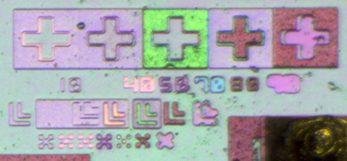
So today let´s start with an old wafer built at the "Werk für Fernsehelektronik Berlin".
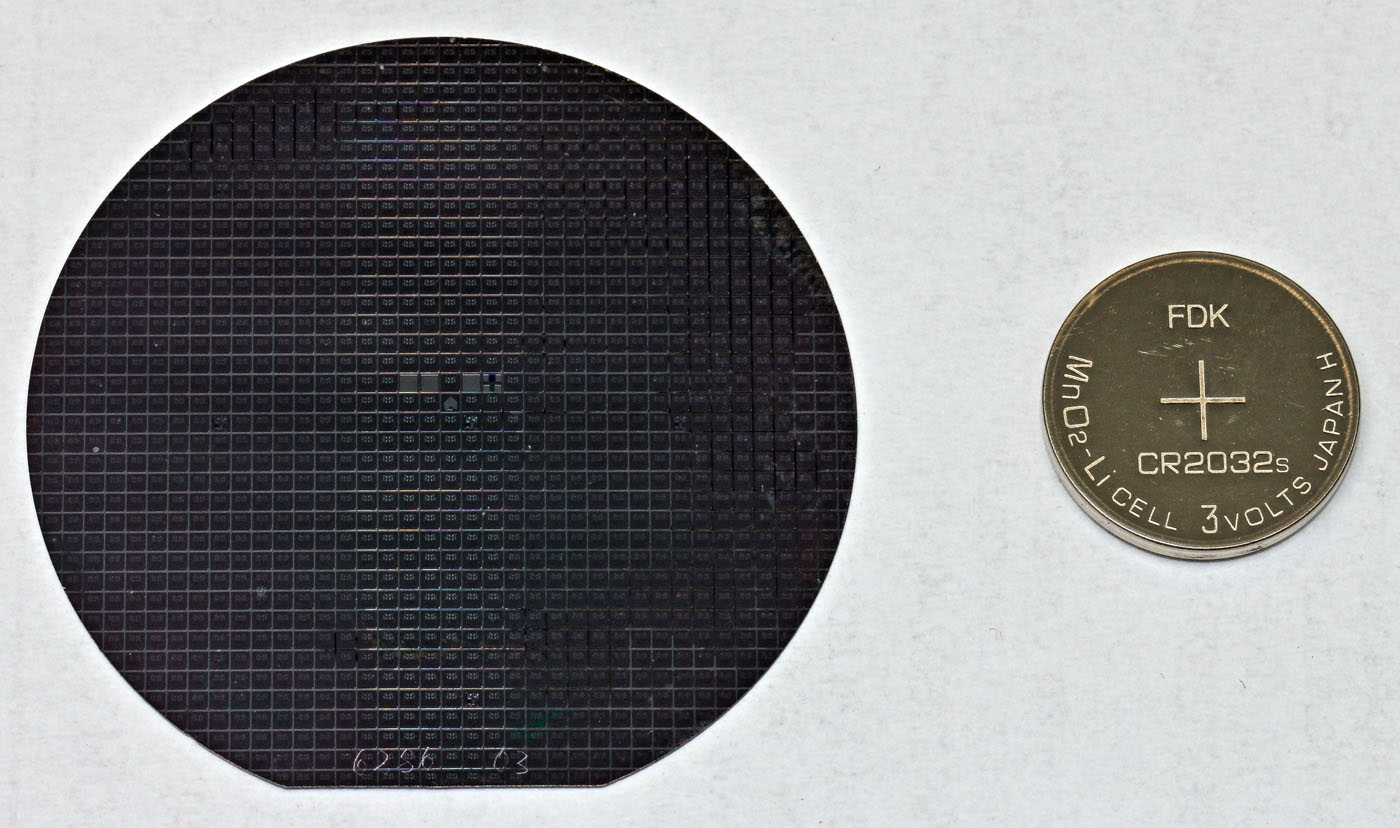
50mm and a die with a edge length of 1,2mm that still gives you over 1000 chips.

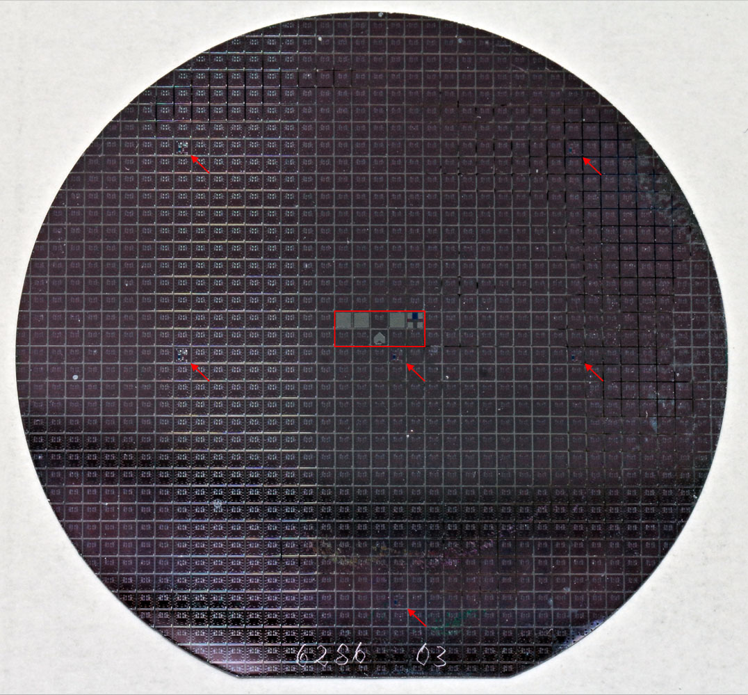
The wafer contains six test structures and some big things in the middle.
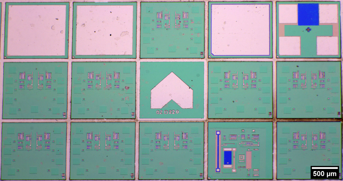
I assume the squares are some kind of etch markers.
The wafer was nearly done only the metal layer is missing. Well that gives some interesting pictures.
Unfortunately I don´t know which chip they tried to build here.
Nice!


More pictures here:
https://richis-lab.de/wafer.htm 
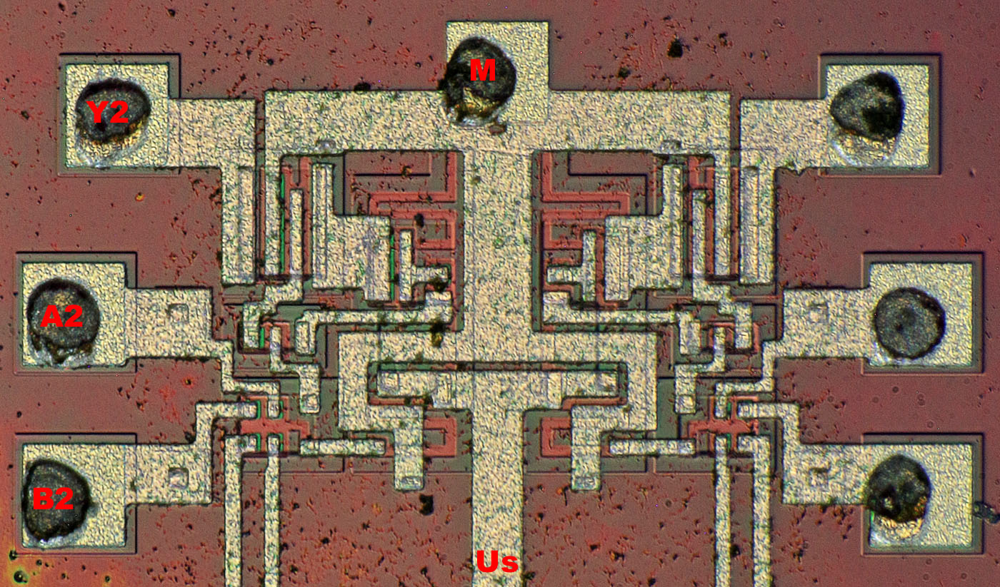
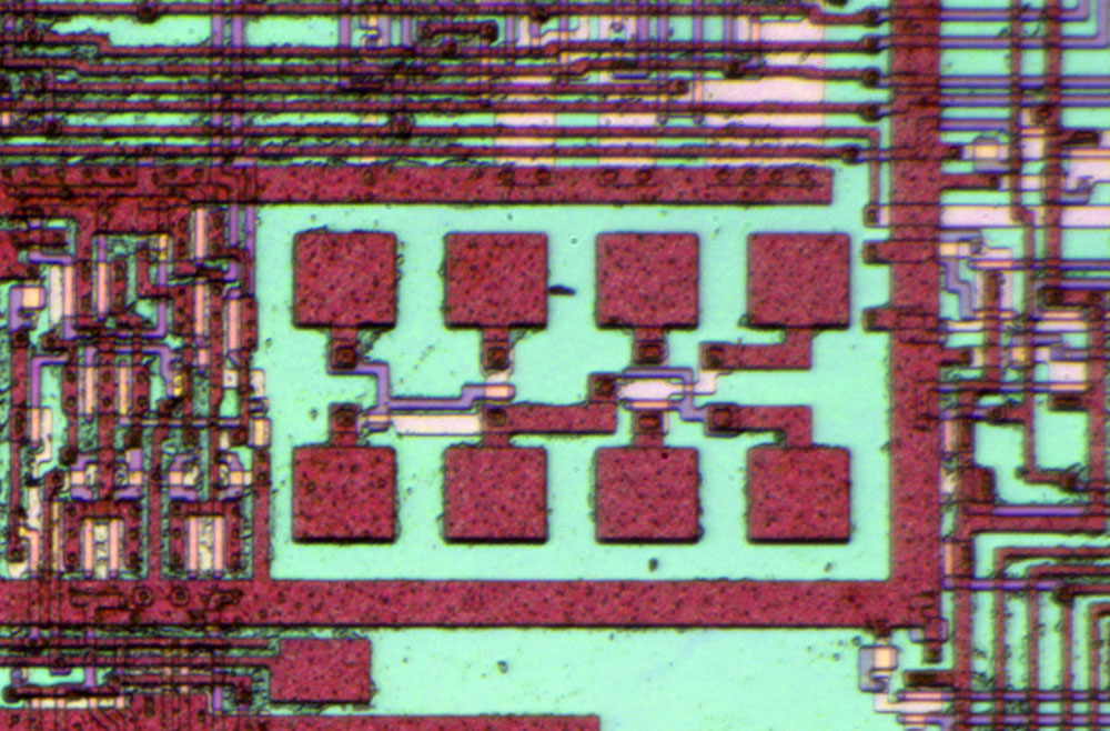
Maybe some very minimal bangap reference? But it's just 4 (5?) NPNs, it's nuts.
I think some current sources or thermal sensors might work on similar principle. No idea why it seems to be a dual.
Maybe just a random test wafer, never meant to even resemble any commercial IC product.
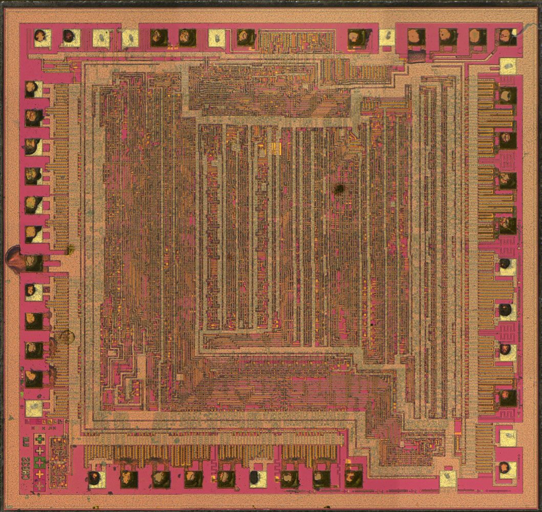
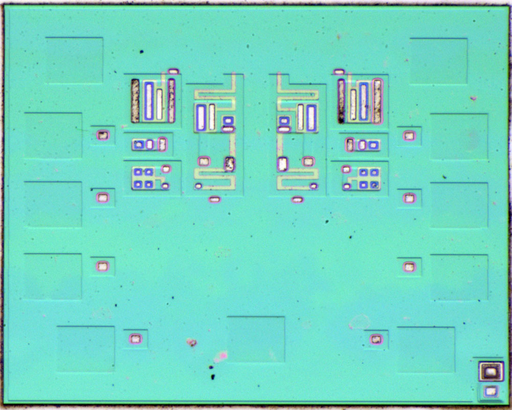
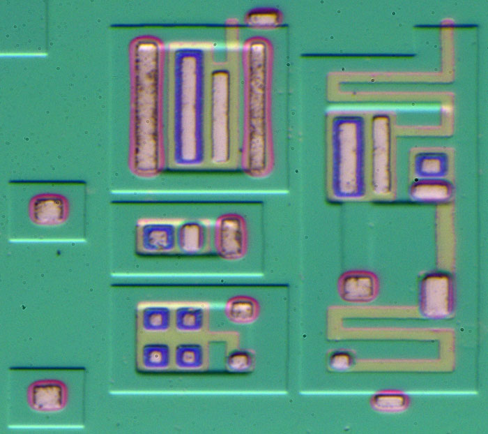
It´s a D220!
=> Two 4-Input-NANDs
I also thought about a bandgap reference

but the 4-emitter-transistor is used for the 4 inputs.
I completely forgot about those

edit
Makes perfect sense
The diodes have to be input protection, the empty area is simply there because bonding pads take too much space.
Today I have a e-ink-display-controller for you. It came out of a watch (Crell NC-7279-919).
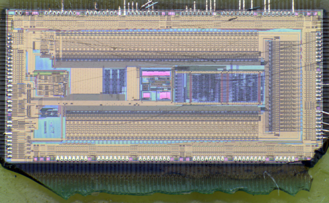
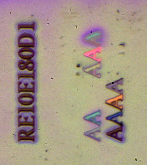
RE10E180D1?

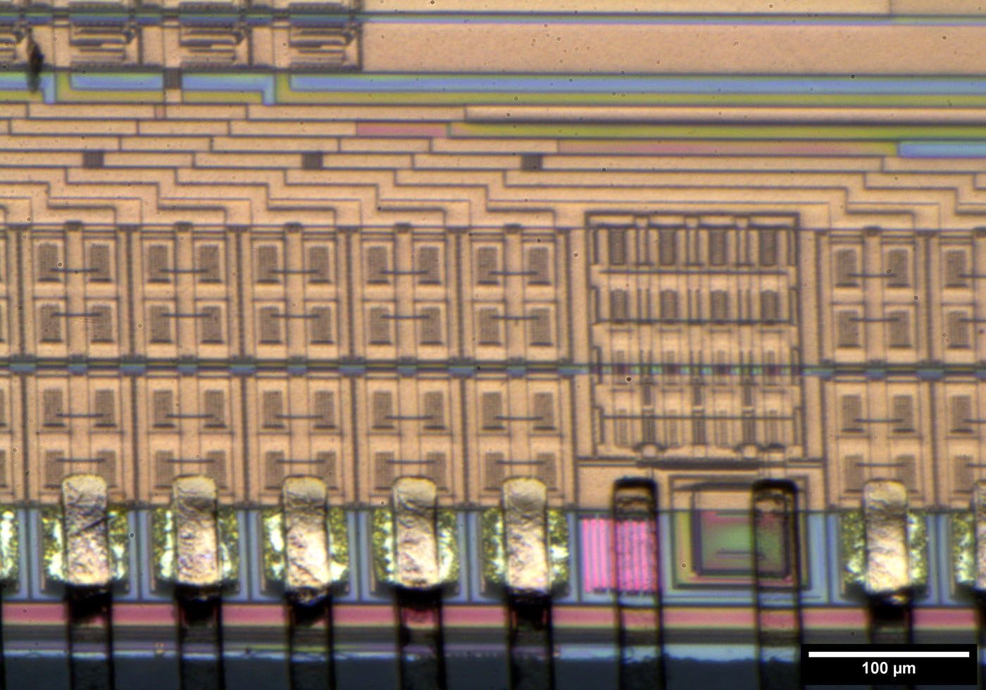
I assume these structures are esd protection circuits.
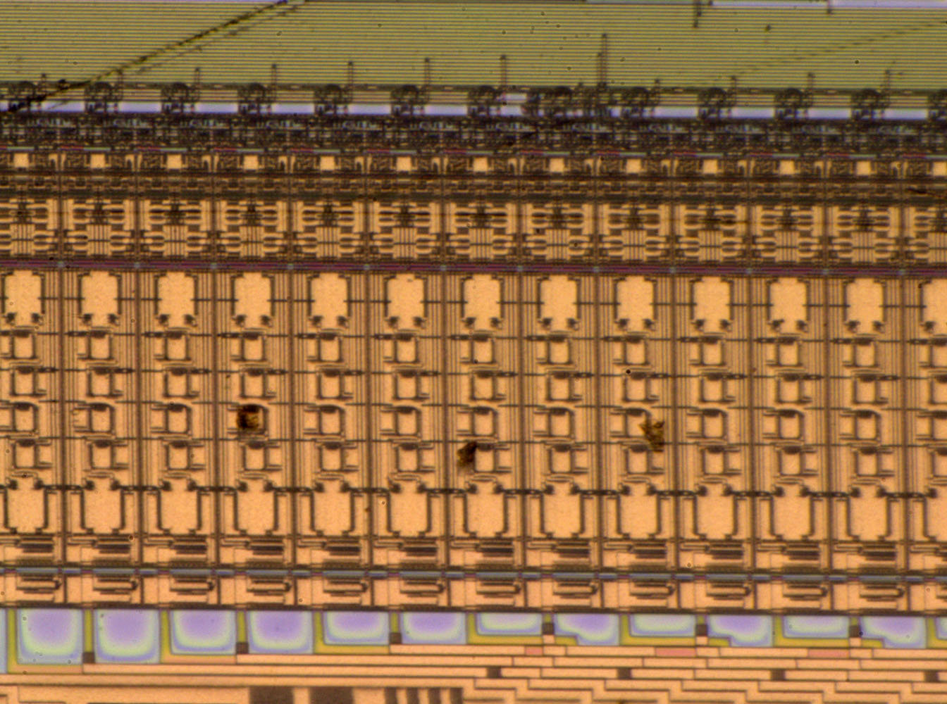
I assume these structures are the output stages and some memory for every output.
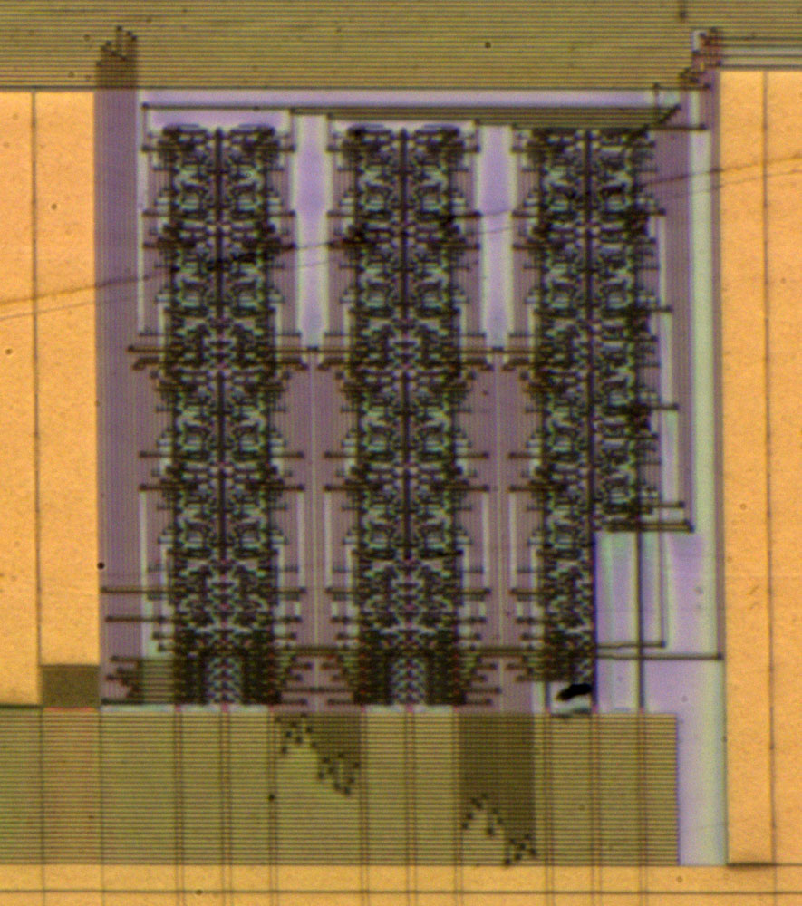
Some Gatearray-Logic.
Perhaps a clock generator?
Some more pictures here:
https://richis-lab.de/E-Paper-Controller.htm
Not matching the number, but could be a MCU from Renesas:
RE Family
E-Paper takes a bunch of weird voltages, could be charge pumps or drive transistors?
Tim
Not matching the number, but could be a MCU from Renesas: RE Family
That´s not very likely because there was another IC in the watch which already looks like a CPU. This one has to be the display Controller.
E-Paper takes a bunch of weird voltages, could be charge pumps or drive transistors?
Tim
The "clock generator"? Hm, very small structures for a charge pump.
Supply circuits are perhaps hiding under the area with the metal cover...
You'e probably right. It wouldn't make much sense. It was just a quick shot.
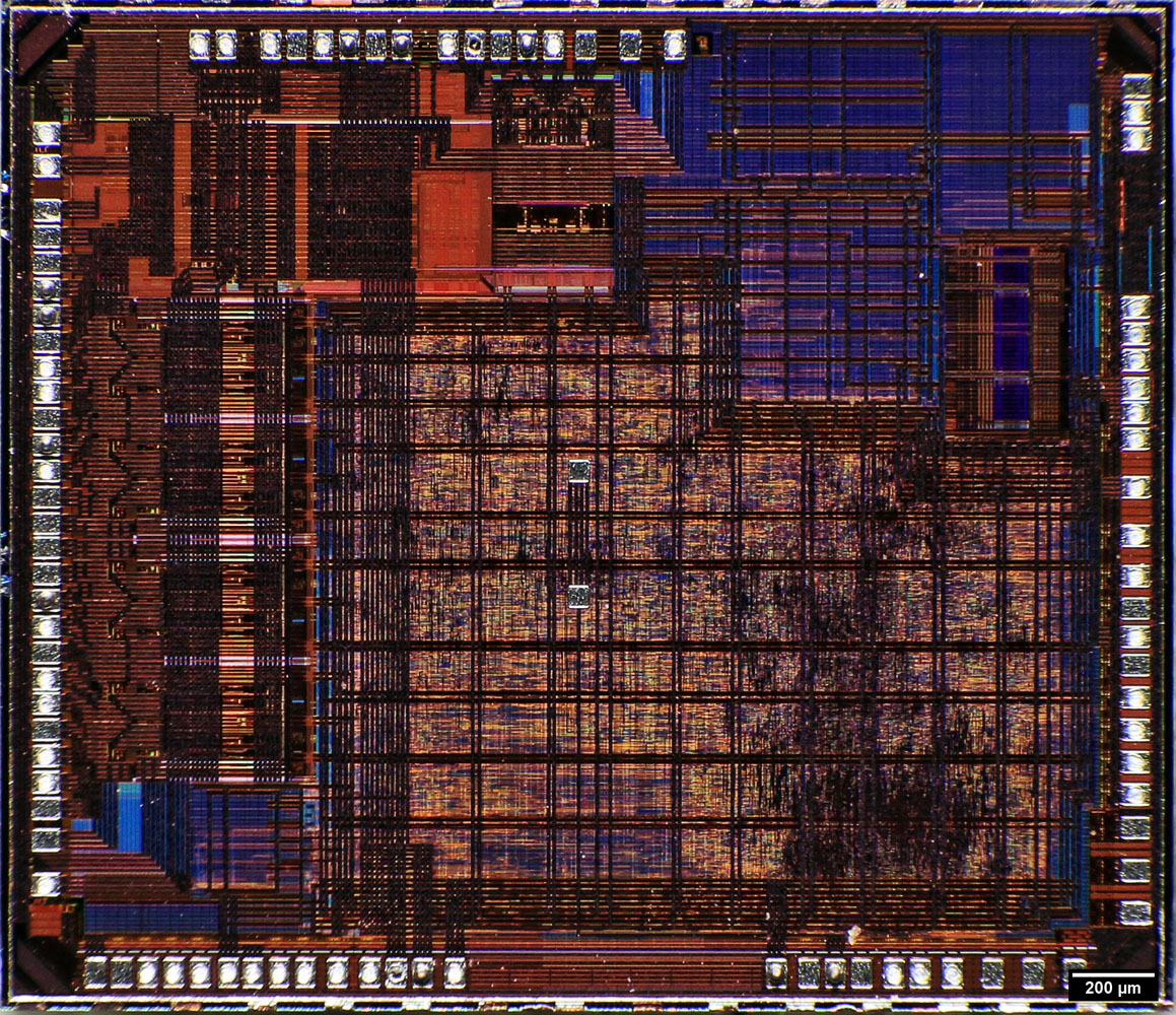
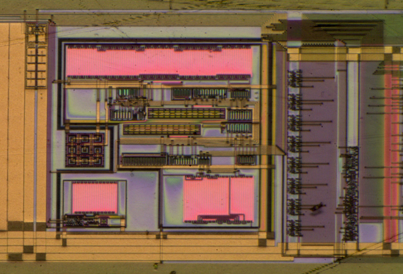
Today the keypad controller TCA8418:
https://www.richis-lab.de/TCA8418.htm
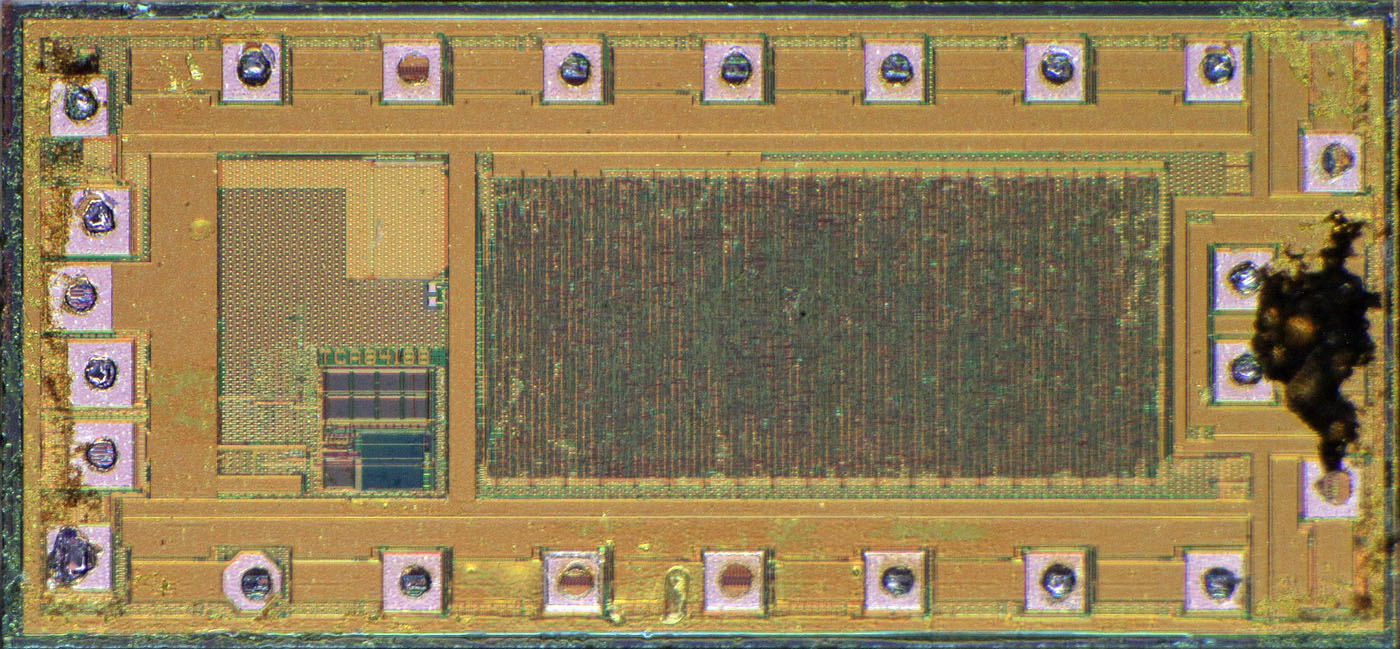
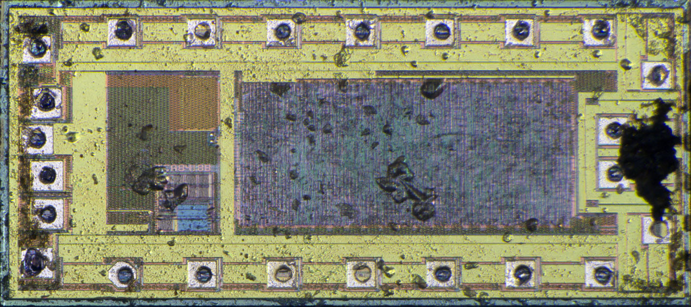
Very small structures and not very good to take pictures of because of the polyimid-layer.
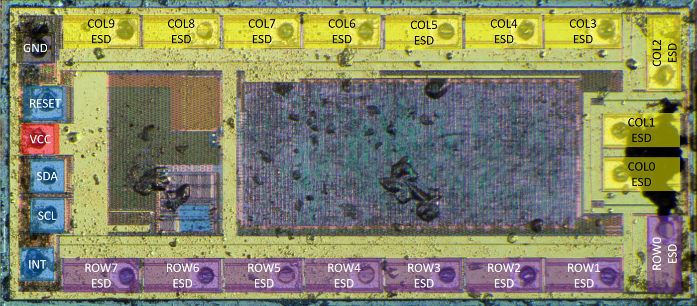
The structures beside the keypad bondpads seem to represent the esd protection. Quite a lot of area...
The right block contains the logic and the left block probably contains the clock generation, power on reset circuit and the I2C-interface.
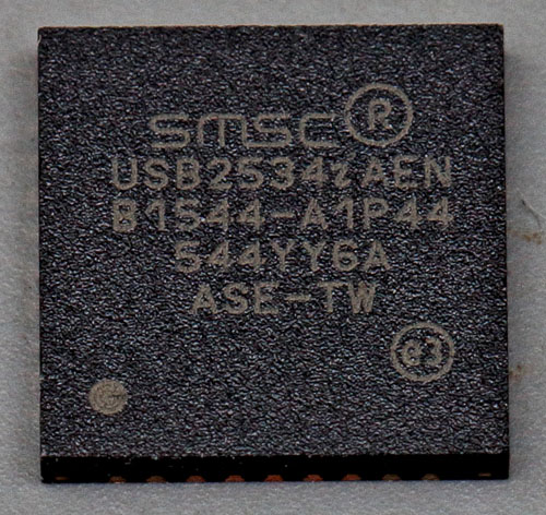
Looking at the usb chip die seems to show how complicated USB is - most of the layout doesn't repeat itself, like a lot of hardcoded logic to handle the protocol
Looking at the usb chip die seems to show how complicated USB is - most of the layout doesn't repeat itself, like a lot of hardcoded logic to handle the protocol
But not every part is for managing the usb, the USB2534 contains also a 8051 controller.

Huh, wonder why it takes so much logic to scan some pins. Also a bit surprising they didn't use diodes into a common ESD structure, I've seen that advertised on a few chips before. Maybe the die is still small enough not to matter. It's only 2kV HBM so it's not very robust for all the area they did spend on it. Also interesting that all pins are individually zenered (or dioded to a common zener rail, but we can see from the die that that's probably not the case), i.e. the voltage limits don't depend on VCC or whatever, it's -0.5 to 4.6V across the board.
Ah, so it's not just scanning, there's a FIFO too; seems it implements quite a lot of keyboard functionality that, in the case of the IBM PC for example, was entirely up to the BIOS to perform. Doesn't look like there's RAM or ROM to control state, so it's either a very compact MCU with ROM scattered around somehow (or hard wired in the sea-of-gates?) or actually all synthesized logic.
Not sure why the I2C side looks different. Is that mesh pattern just top metallization, or is it transistors/interconnects? Almost makes it look like there could be some fat transistors in there, but I don't see any reason why this should have large switching capacity or an LDO or something in it. (Well, I guess the LDO is possible -- maybe the core logic is 1.2V or something? Heh, it does run 1.65-3.6V, a fairly wide range; not unheard-of for logic gates, but also possible this way.) Very low power, fractional mA at worst, a fine-pitch design in any case.
Tim
Also a bit surprising they didn't use diodes into a common ESD structure, I've seen that advertised on a few chips before. Maybe the die is still small enough not to matter.
I assume they wanted a chip which doesn´t need a lot of external components...
Ah, so it's not just scanning, there's a FIFO too; seems it implements quite a lot of keyboard functionality that, in the case of the IBM PC for example, was entirely up to the BIOS to perform.
Probably it should work as a "simple" (in terms of the user) and easy connection between a keypad and a controller.
Not sure why the I2C side looks different. Is that mesh pattern just top metallization, or is it transistors/interconnects? Almost makes it look like there could be some fat transistors in there, but I don't see any reason why this should have large switching capacity or an LDO or something in it. (Well, I guess the LDO is possible -- maybe the core logic is 1.2V or something? Heh, it does run 1.65-3.6V, a fairly wide range; not unheard-of for logic gates, but also possible this way.) Very low power, fractional mA at worst, a fine-pitch design in any case.
I don´t see transistors on the left side of the die but perhaps they are still there.
There should also be some clock generator, output stage for I2C and undervoltage detection. Some housekeeping...
Had some other thoughts -- the sea-of-gates approach seems wasteful for a one-off. But I wonder if it's not, if it's designed as a I2C interface ASIC and they use the same 20-GPIO format across many parts? Saves on masks. That maybe explains the pins taking up so much space, as they're left general-purpose for any ASIC design. Maybe if you look at other parts in the same I2C interface family, same or lower pin count, you'll find exactly this?
Tim
I´m not sure about that... Isn´t a gatearray a quick solution to solve problems. There might be a more efficient way to integrate the logic but probably engineering time costs more than the silicon area if you built a special chip.
In mouse sensors (
https://www.richis-lab.de/mouse.htm) you often see integrated gatearrays:
Wanna see the internal of an optocoupler? I have a H11L1 for you:
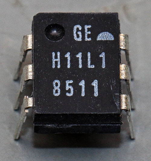
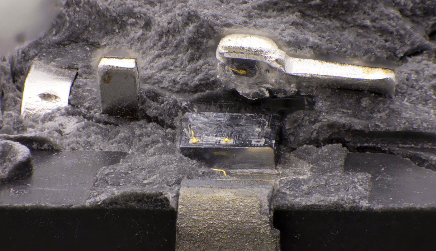
The LED is placed above the receiver on a bent part of the lead frame.
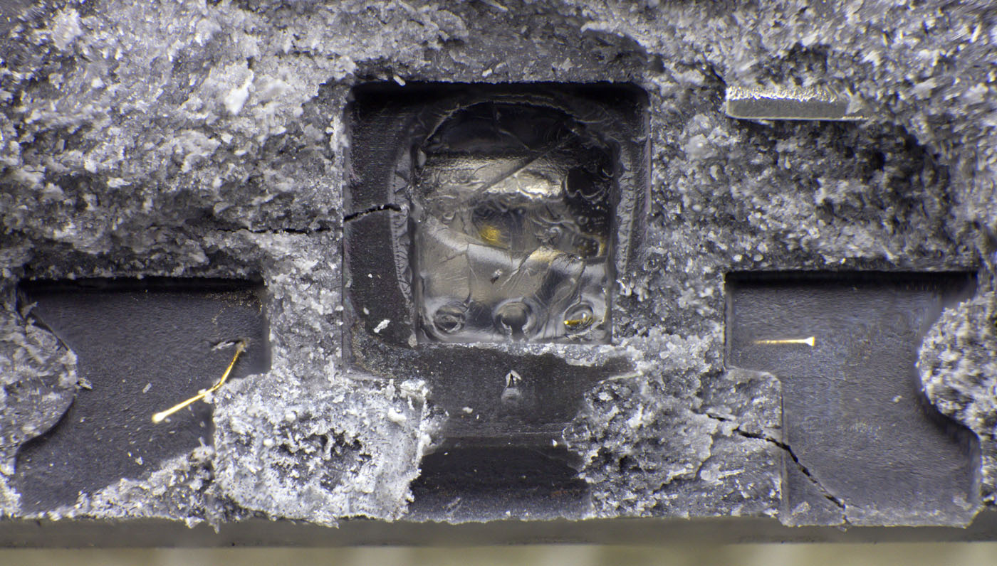
If you just break out the receiver you can look onto the square routing the light and containing silicone.
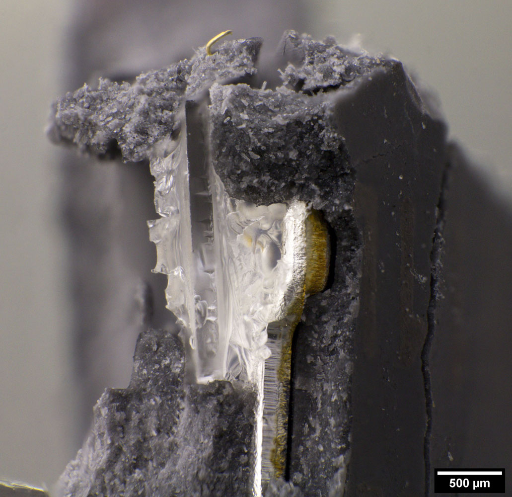
In the path of light there is also some glass (0,17mm).
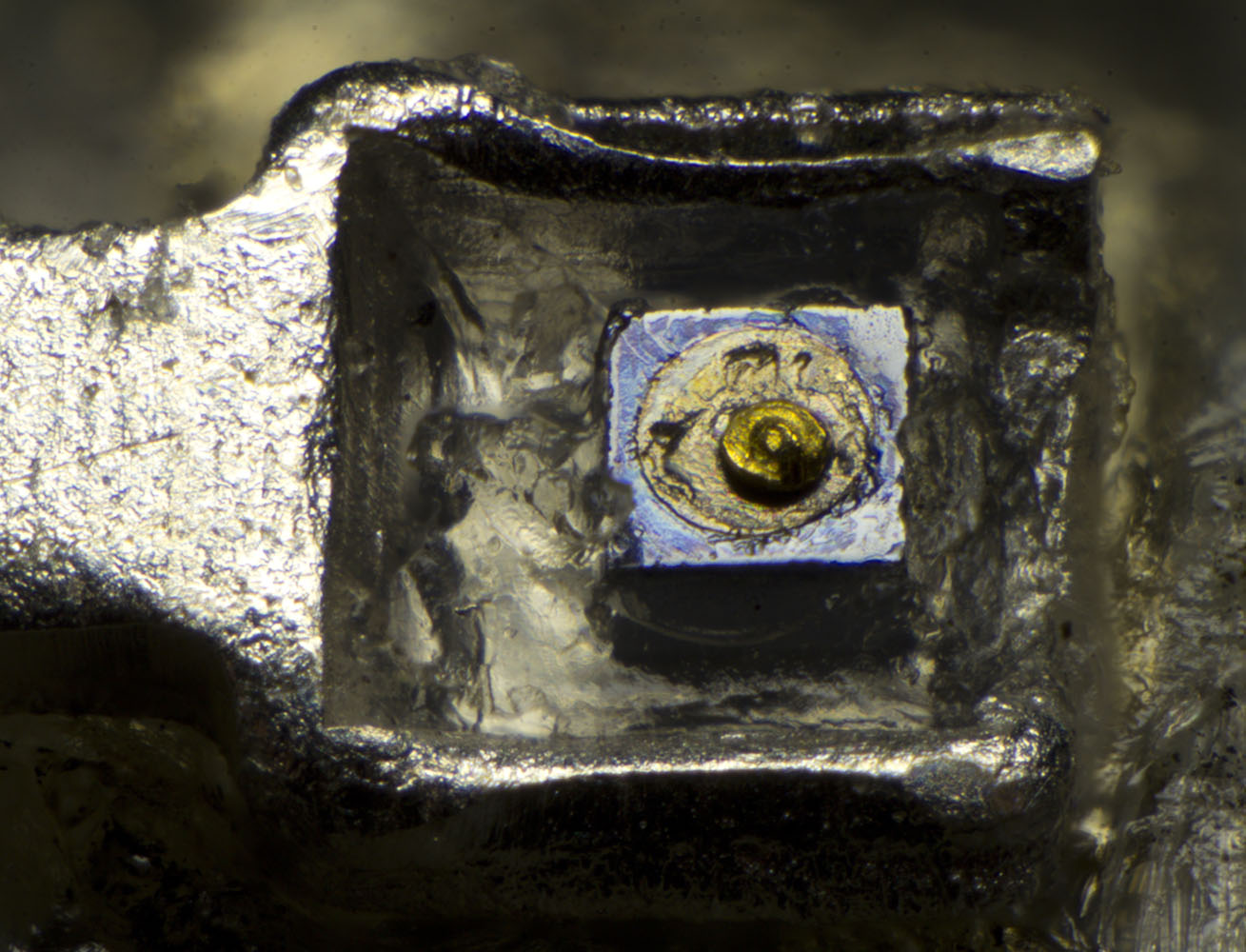
The LED is 0,3mm*0,3mm and owns a quite big metal contact.
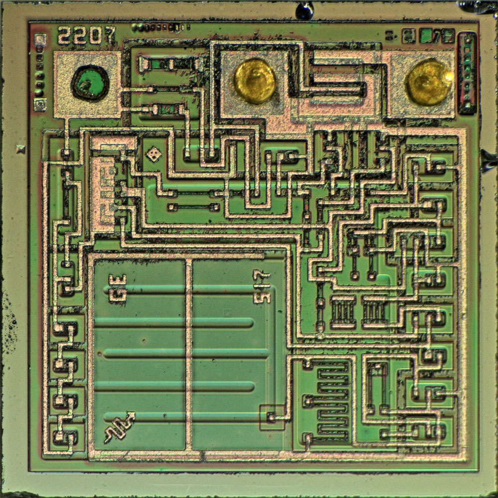
The H11L1 uses a optical diode, not an optical transistor. (Nice light symbol.
)
Silcon art, yeah!
More pictures here:
https://www.richis-lab.de/Opto01.htm
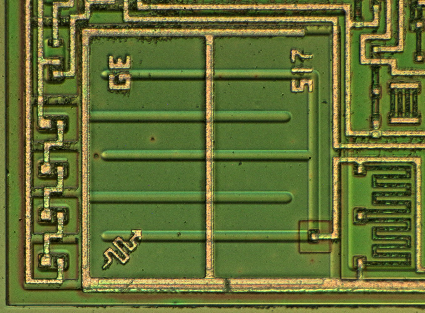
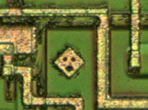
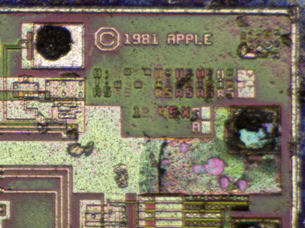
For the Apple fanboys I have a 344-0022, the IOU (Input/Output-Interface).
With the MMU and a PAL the IOU manages the memory and the input/output adressing.
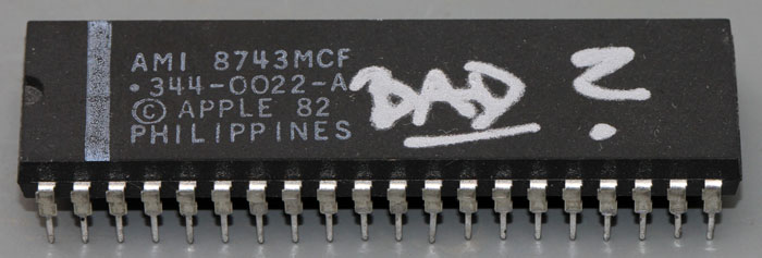
The packages tells us that the 344-0022 was produced by AMI in 1987 and that it was designed in 1982.
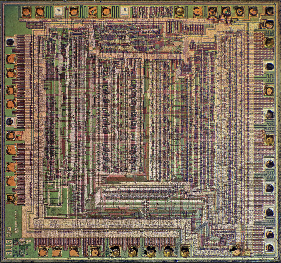
The die is 3,48mm x 3,25mm. The smallest structures are roughly 6µm.
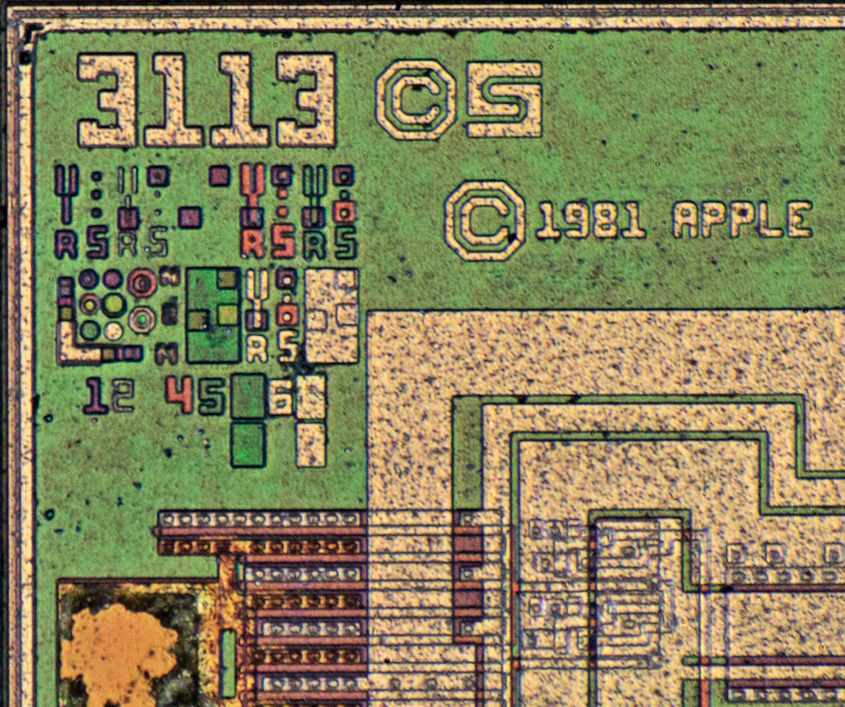
On the die you can see five masks. The "R5" for every mask could be a hint for a fifth revision. Perhaps...
The S stands for Synertek. I assume Apple designed the features of the ASIC, Synertek designed the chip itself and AMI produced the ASIC.
The "Apple-copyright" on the packages (1982) doesn´t correspond to the "Apple-copyright" on the die (1981).
Today I have the second Apple-2-ASIC for you, the 344-0011:
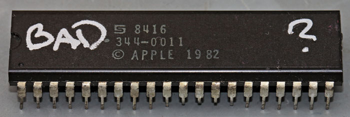
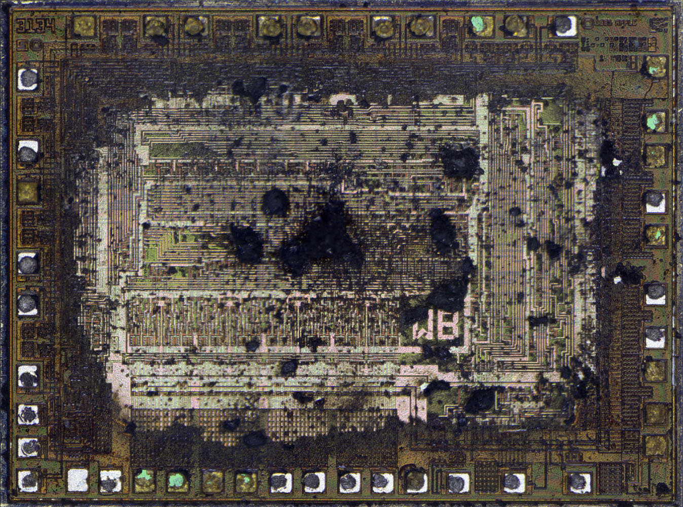
The polyimid finish is quite persistent but:
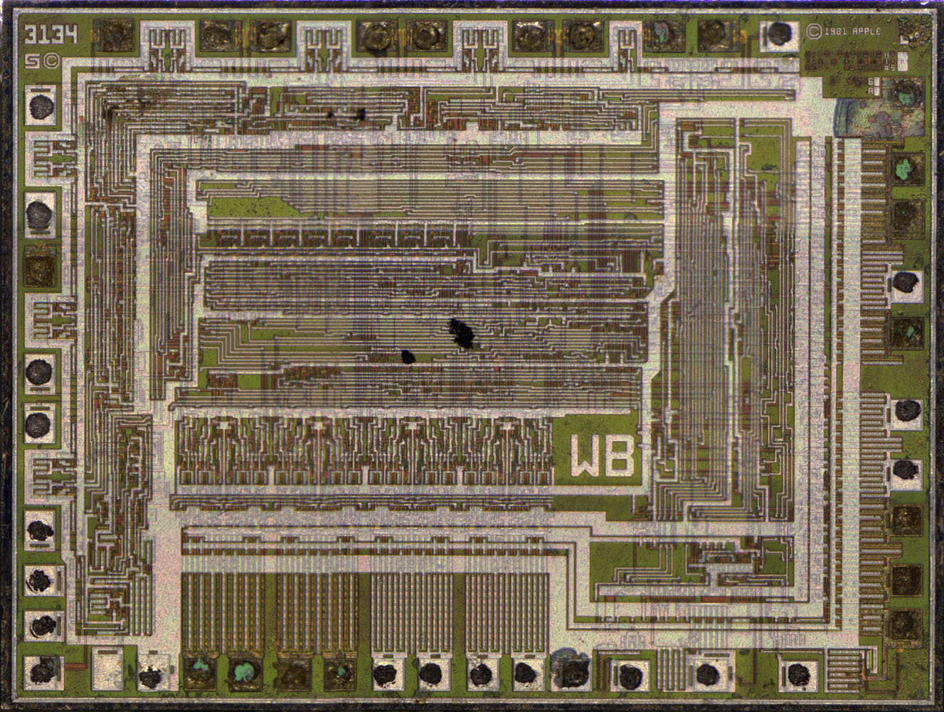
WB? Probably the developer...
It seems there is one mask more than in the 344-0022...
https://www.richis-lab.de/apple.htm
And here the 344-0011 clone built by Mikroelektronika Botevgrad, the CM631:
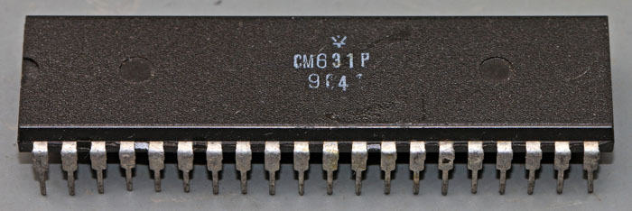
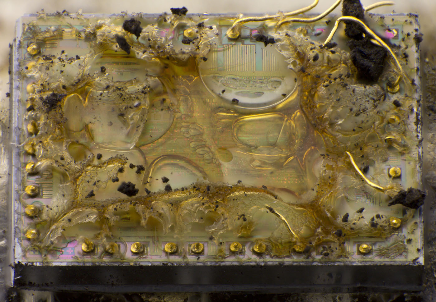
I found an interesting die coating. It was a sticky stuff resistant against high temperatures but I was able to rub it off the die. Some isopropyl was a help but I assume it wouldn´t have been neccesary.
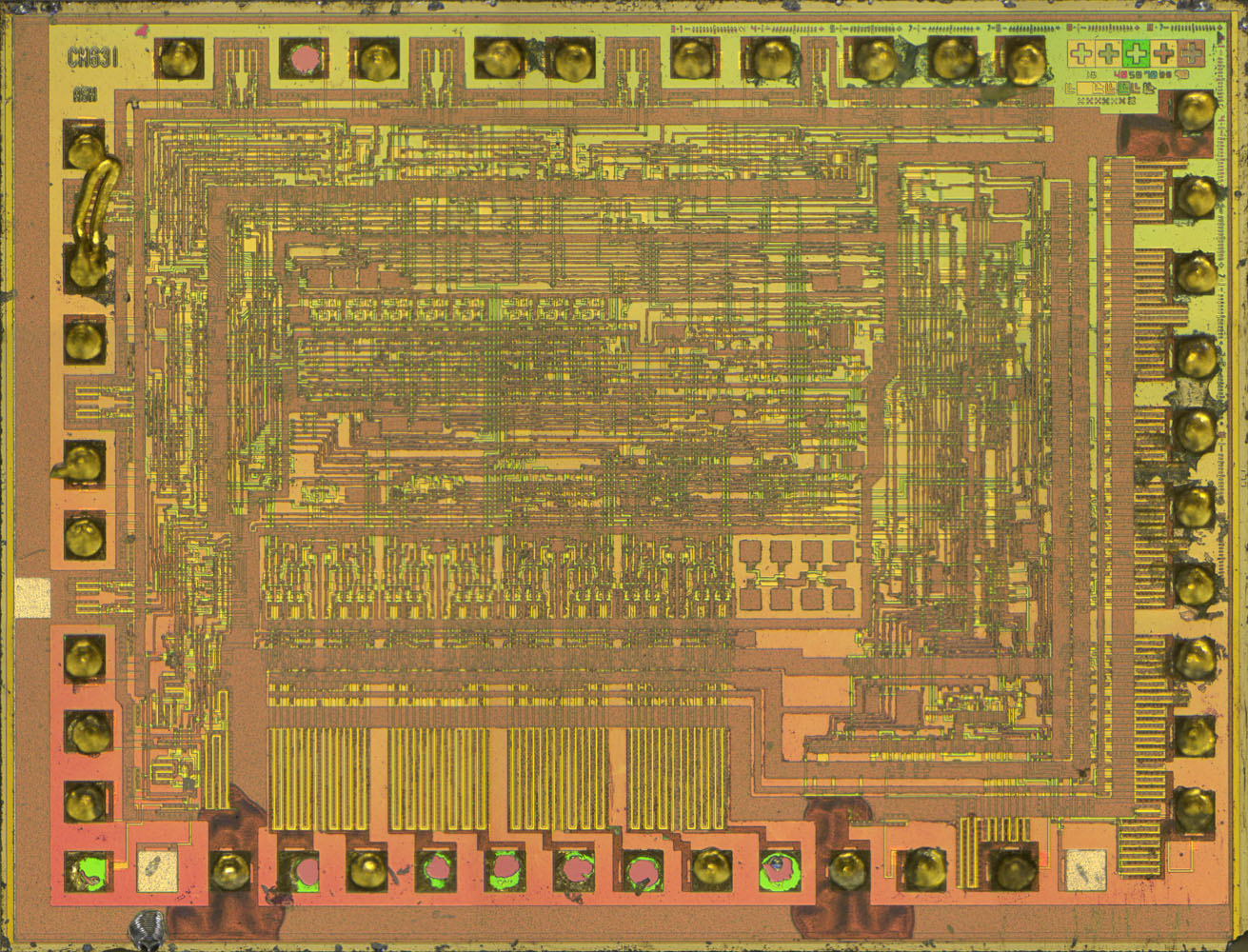
As the CM632 the CM631 is quite similar to the apple original but it´s not exactly the same.
...
Test structures!
https://www.richis-lab.de/prawez03.htm
Richi,
Let me express my gratitude and congratulation for the job you are doing!
I guess you can be a very interesting guest in an episode of the Amp Hour podcast!