-
My first though is that it looks like you have a switching DCDC converter, not sure of the current/power requirements but if it was me I would try connect each component that is part of the power path with a thicker track or a plane like this:
Yes I thought that might come up. I'm just not quite sure how to do it in Altium other than by literally drawing the polygons, and I can see them ending up rather ugly :-)
I might have a go though.
It's an AP5724 DC to DC converter. http://www.internetsomething.com/lcd/AP5724%20backlight%20driver.pdf
There's 6 LEDs in series, at 20mA, 18v total, so 360mw total. They say the above driver chip is 84% efficient, so expected draw of 430mw. Call it 500mw. I'm not really sure I know enough about this stuff, but I gather it's current that matters. So the 500mw should pull 151mA from the 3.3v supply. I've used 10 mil traces which an online calculator says should be good for 450mA with 1oz copper. The LCD panel itself pulls 15mA. So I'm at about 165mA.
What do you think? I suppose it makes sense for me to learn how to do the job properly though doesn't it..
The way I see it if the LED's expect to consume 360mW and the converter is 84% efficient then this means 70mW will be dissipated as heat in the SOT23-6 package. Given that θJA is 162°C/W this means that IC will rise by ~11°C above ambient. Not that bad but for the sake of it I would still use a polygon to help dissipate the heat, and give the current a much less resistance pathway (lower ohmic loss, not that it matters that much with your current draw).
As for polygons you can either manually place them down and adjust as you go like:
Or you could use another layer (like MECH 1) to define the shape and then create a polygon on copper layer, like (Create Polygon from Selected Primitives): https://www.altium.com/documentation/15.1/display/ADES/PCB_Cmd-ConvertSelected((ConvertSelected))_AD
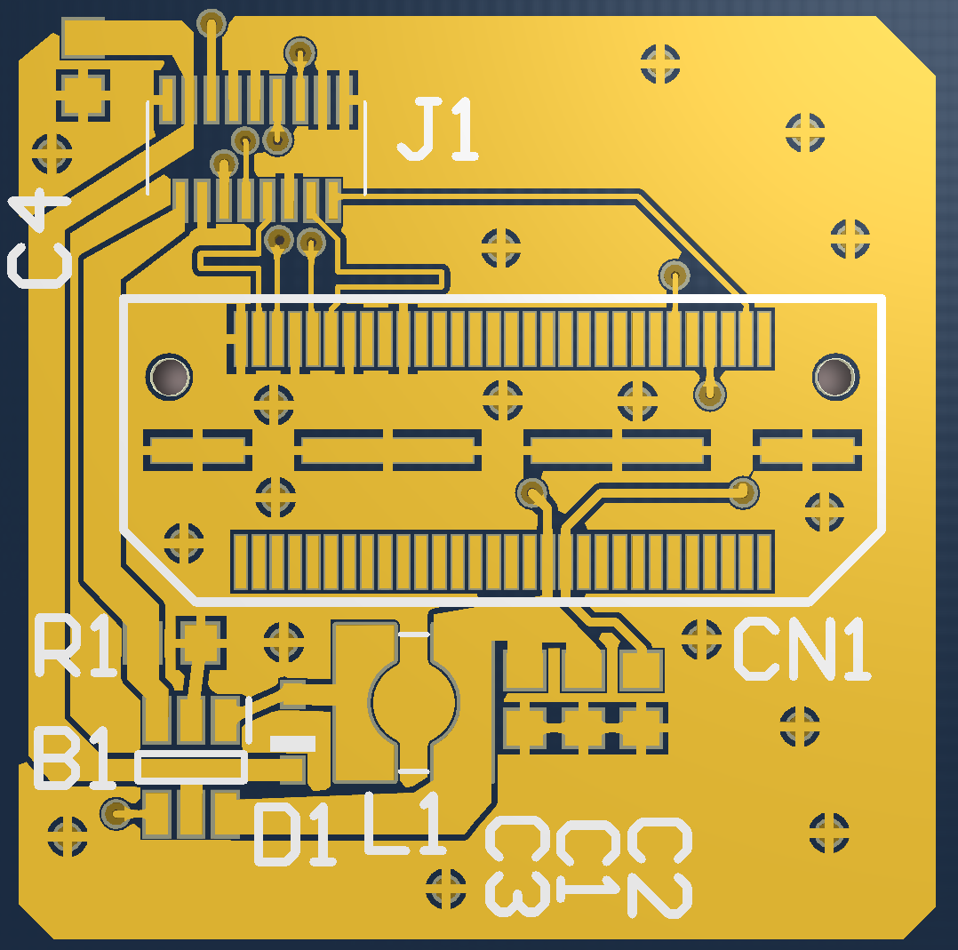
Also I think your latest iteration with polygons looks better, but there is still room for improvement. To get an idea of a good layout have a look at the appnote:
https://www.diodes.com/diodes-part-files/AC/AP5724/User%20Guides%20and%20EV%20Boards/AP5724-EVM.pdf
Notice how all components part of the power path (inductor, diode, filter caps, IC...) are all connected via a large polygon
Thank you. I didn't think of dissipating heat with pads/polygon.
The reason my +3.3v polygon doesn't continue through the diode is because the LED driver datasheet specifically says to minimise trace width here.
However, I may be misunderstanding. Perhaps it's just the trace from the diode to the IC that needs to be minimised, and maybe I should still have a fat trace (polygon) from the inductor to the diode.. but then.. isn't the effect the same?
-
The current paths in that SMPS look unnecessarily long. You want the high currents to have short, uninterrupted current paths from the input capacitors to the output capacitors.
You could improve this by rotating the inductor by 90° clockwise and move those input capacitors closer to the output caps. Also, fatten the traces up around the diode.
I'm not clear on how to do that :-/
What about moving output capacitor C4 up top by the LCD socket? Would that be an improvement? -
I think they mean trace area going into SW pin, if you have a look at reference design they still have a wide traces for all components it's only when they funnel into the IC that they become smaller (design constraint of pin positions).
Also Dave made a good point. Think of a transient happening on the Vout and suddenly you must supply additional current to get the voltage back up, how you have C4 positioned makes it harder for the circuit to respond faster.
-
I think they mean trace area going into SW pin, if you have a look at reference design they still have a wide traces for all components it's only when they funnel into the IC that they become smaller (design constraint of pin positions).
Also Dave made a good point. Think of a transient happening on the Vout and suddenly you must supply additional current to get the voltage back up, how you have C4 positioned makes it harder for the circuit to respond faster.
I hear ya. I did think that C4 might need moving closer to the LED backlight. I just wasn't sure about moving the other caps or re-orienting the inductor... too much brain power required at this stage!
The whole thing is super tiny mind you - if that makes a difference. In fact I forgot how small it was, and I have just spent ages lengthening the pads on the small LCD connector at the top so that I have a better chance of soldering it.
Here's the latest iteration/changes then.. Hopefully it'll do the job. I forgot to re-apply teardrops, but I'll do that later.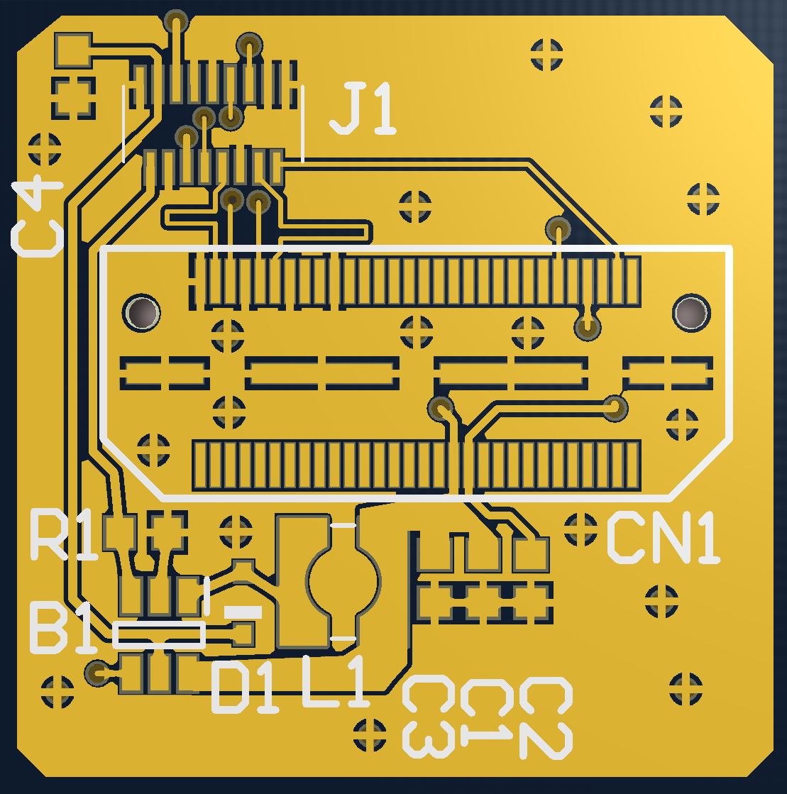

-
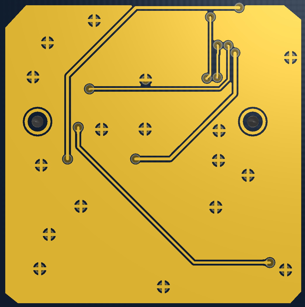
Any better? : C4 only has that one 12mil via to ground. Do you think that's a problem? I suppose I could simply make it a bigger via. Otherwise, if it matters, I'd have to look to get the ground pour to reach around.


-
nevermind, I have sorted that ground pour for C4
-
I've got an important question.
C1 (100nf) and C3 (1uF) are in parallel, right next to each other.
This is because the original schematic had C1 on the power into the board, and then the datasheet schematic for the backlight driver had C3 (1uF) in it.
Should I ditch one of them? Obviously this elementary question will highlight my naivety and lack of knowledge on basic electronics :-/
I have beefed all the caps up to 0805s, for ease of placement, and availability on the higher voltage side (~18 - 20v). -
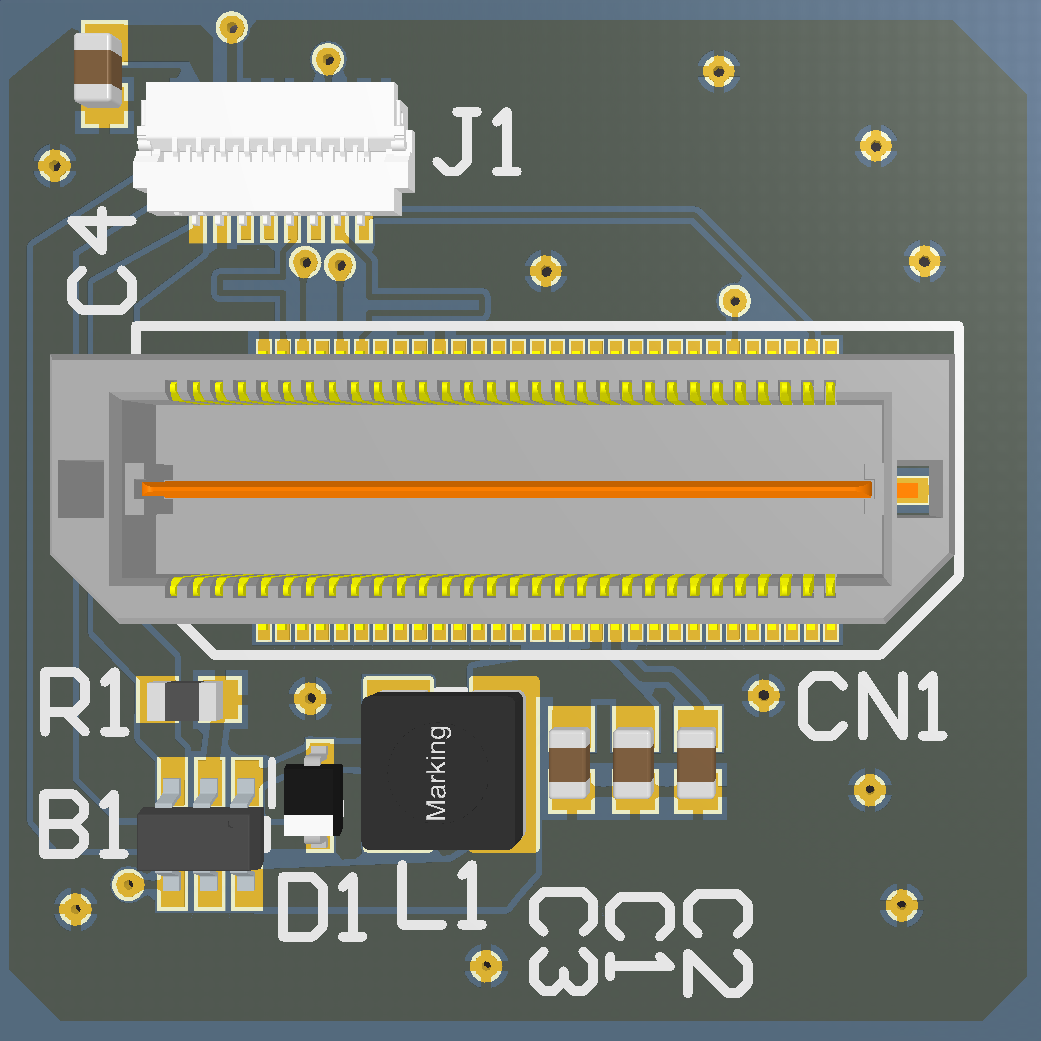
If J1 is a single sided flex cable connector, the pins where you length equalize extended the traces may travel into the connector to the flex cable with a little more length inside the connector compared to the pins right under the connector. Have you taken this into account when extending those 2 traces to their length on the PCB?
-
If J1 is a single sided flex cable connector, the pins where you length equalize extended the traces may travel into the connector to the flex cable with a little more length inside the connector compared to the pins right under the connector. Have you taken this into account when extending those 2 traces to their length on the PCB?
Hi. Do you mean that they may have already compensated for the connector pin separation in the flex cable? -
boards have come out looking reasonable, and the pads line up too

I'll report back if they actually work, once I've finished my reflow oven.
-
So it turns out I had the LCD pinouts back to front

My first attempt at reflow soldering went well. Little bit too much paste - bridge on a pin that didn't matter.
but the LCD backlight driver didn't work. Progress was hampered by the fact that I've only ever done Arduino. Between Keil and TrueStudio, I had a hard time getting the discovery board example programs to compile. I needed them to compile so that I could add in an 'HAL_GPIOB pin1 enable' thingy.. i.e. turn on the LCD backlight, since the examples are all meant for the amoled screen with no backlight.
I did some playing. In fact I burned out one of my LCD flat flex by sticking a li-po on it and getting the polarity back to front. I guess this is why I need a current limiting power supply. DP711 or DP832 though.. ? DP832 is more money but crucially its kind of huge
Anyway then I constructed a better test.. 5 plain LEDs wired in series on some breadboard, to be driven by my little circuit. and it worked! 3.3v in, drives 5x LEDs nicely.
Then I looked closely at the LCD datasheet for the FFC pinouts and it looks like I had it the wrong way up. Well, what I mean is that I assumed the FPC to be going in the connector at top-contact rather than bottom contact. So pins 1-17 should be pins 17-1 instead. Left to right-flip.
I don't think this is fixable. So I have 49 keychain PCBs
In all honesty, it quickly became apparent that I have made myself a PCB here that's very difficult to debug (since it's face down when fitted to the ST Discovery board). Perhaps I'll spend a bit more time on rev 2 and put some test points, as well as maybe more than one type of LCD connector. -
Checking over my designs and I can see why it's happened. I used Molex 504281-1700 in the design, which has contacts on both top and bottom. I have 5 of these connectors. I actually fitted a flip-connector though (Amp 10061122-171120HLF), which seemed to grip the FPC better, and was dirt cheap. These are bottom contact only. So it might be Ok after all if I use the other connector
-
Did you protect your I/O? I did not look at it but there might be special things you need to do if that chip is the first thing in the circuit connected by a wire.
And how is that board being mounted mechanically? I don't see any screw holes. I assume it clips into a assembly some how? Keeping it stationary is important.
-
Hi. The Samtec DSI connector makes a tight fit!
I'm just reflowing a second attempt now. I had some 17-way 0.3mm top contact flip connectors.. unknown brand from Aliexpress. Just trying again with one of those
I only have one more of these LCD panels left though
-
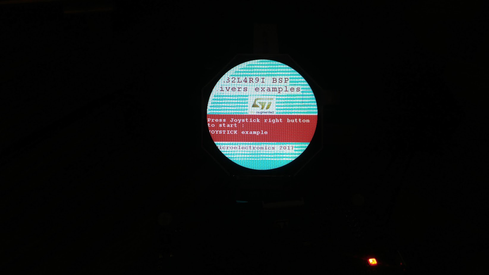
Sweet. It works!
There were a couple of solder bridges there which were on unused pins, but I've wicked them out now anyway.
Just need to figure out what needs changing in the LCD driver code now !
This is a marked improvement from a couple of hours ago where I thought I'd designed the pin outs back to front and would have to re-do the design!

-
Well, something's happening. The thing is, I can't make sense of all the DSI init commands in the example code. I just don't know how the sequence works. Having spent about an hour reading data sheets and still not really understanding, I removed a load of the init commands (which aren't meant for this screen), and I got this:

then I removed some more, and now I have this

-
Now I have added in a command, and it works as per the data sheet. Yay. MADCTL, x-mirror, etc.
-
So close now.
I think all that's wrong is the GFXMMU thing that basically manages memory (framebuffer) usage for circular displays. It chops off bits or something. I dunno. Well anyway it all looks good so maybe I should move onto the StEmWin stuff.
-
I realise you now have your boards back (and they work! awesome!
 ) so it's probably a bit too late, but... why do you have thermal relief on your stitching vias?
-
I realise you now have your boards back (and they work! awesome!
) so it's probably a bit too late, but... why do you have thermal relief on your stitching vias?
What's that then??
Is that something to do with the vias looking like a cross-hair? (I have no idea why that is.. Altium just did that). -
Another weird thing is that R1 footprint.
It's a metric 1608 (should be same as an 0603) from the Cern Altium library. The footprint looked like an odd size in the end though and I've actually put an 0805 resistor on there. I've done two of the boards now and it seems to fit OK. All the caps are 0805 anyway. Sort of figured there might be less chance of tombstoning with bigger bits / more paste etc. -
That has worked out remarkably well for a first PCB. In the future I would suggest using thicker traces in the switching regulator area, and keeping everything as short as possible there but it seems it has worked out ok in this case.
-
That has worked out remarkably well for a first PCB. In the future I would suggest using thicker traces in the switching regulator area, and keeping everything as short as possible there but it seems it has worked out ok in this case.
Thanks for the tips. Yes I'm pleased! I did burn up one of my LCDs mind you. Thankfully just as $25 one.
I really do need to get a current limiting PSU that doesn't take up half a desk.. I might look at those modules that Dave reviewed some time ago. Those all over eBay. -
Last pic, cos I'm super chuffed

-
That looks really good, it's always very exciting when a complex display like that actually works. That would make an interesting analog style desk clock or weather station, I've always been fond of analog dials.