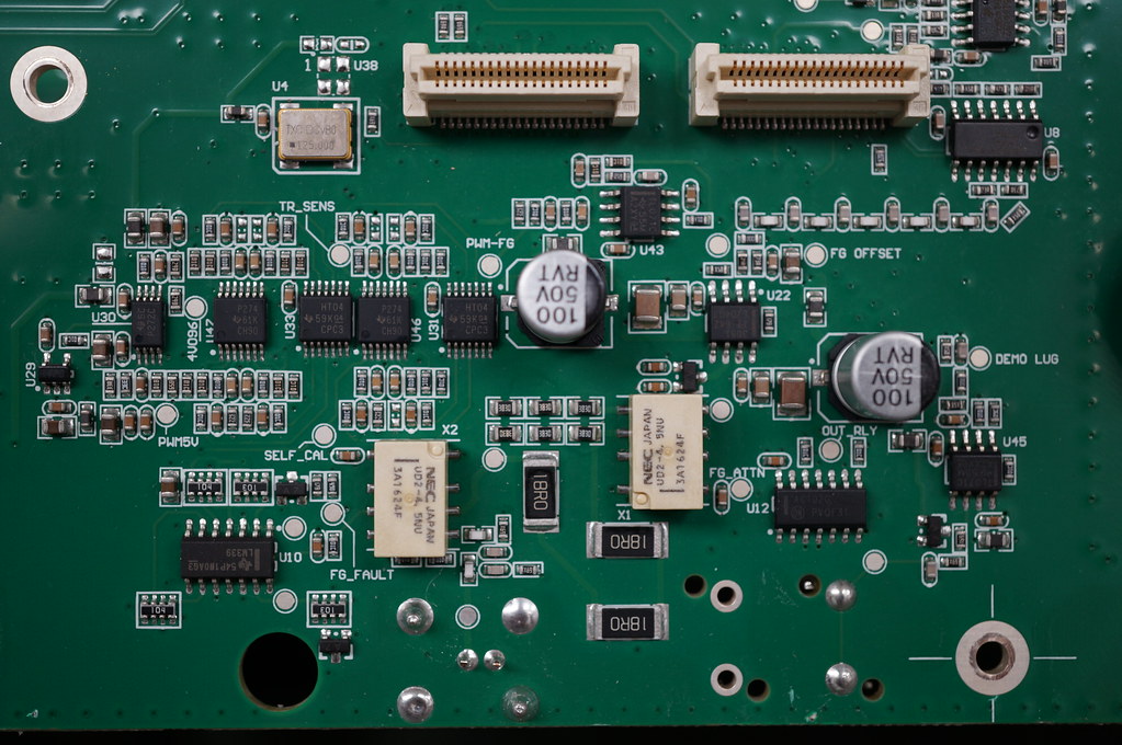
I just noticed there is no DAC for the function gen - looks like it uses PWM from the FPGA.
Or maybe R/2R from the FPGA?
Don't see a benefit to that as it needs precision Rs and very stable outputs. The FPGA could be doing PWM ( or some other modulation ) at a few hundred MHz, so 20MHz ( max the wavegen goes to) would be easily doable. There is a multistage LC filter in there.
I noticed that filter.
 Keysight 1000 X-Series Oscilloscope Teardown
 by
Dave Jones, on Flickr
Did they use a DAC on the 2000/3000X? I don't recall.
If so then another obvious cost saving measure.
Does the test point labelled "PWM5V" give any hints?
I just noticed there is no DAC for the function gen - looks like it uses PWM from the FPGA.
Or maybe R/2R from the FPGA?
Don't see a benefit to that as it needs precision Rs and very stable outputs. The FPGA could be doing PWM ( or some other modulation ) at a few hundred MHz, so 20MHz ( max the wavegen goes to) would be easily doable. There is a multistage LC filter in there.
I noticed that filter.
Keysight 1000 X-Series Oscilloscope Teardown by Dave Jones, on Flickr
Did they use a DAC on the 2000/3000X? I don't recall.
If so then another obvious cost saving measure.
Can't find your pics - had a quick skim of the vids & didn't see a similar filter
incidentally your teardown stills are is something I've had problems finding in the past - maybe you should add an index of the hi-res pics on the eevblog site, AFAICS they're only linked from (some of) the videos
Does the test point labelled "PWM5V" give any hints?
Maybe - I was playing with it on a desk that too far away from my main a scope, and it was too fast for the 1000x to probe itself!
Will look into it some more soon.
Does the test point labelled "PWM5V" give any hints?
I figured that would've just been a power rail, there is one labeled "PWM-FG" though
I would not be so hard against the powersupply. I had to fix the powersupply of rarely used Tektronix TDS2012 a few times and i don't think that the tek-powersupply had a better quality. If i remember correctly the problems there were mostly broken solder points
I would not be so hard against the powersupply. I had to fix the powersupply of rarely used Tektronix TDS2012 a few times and i don't think that the tek-powersupply had a netter quality. If i remember correctly the problems there were mostly broken solder points

One I have here (2012B) at least has caps that I've heard of before, mostly Rubycon but still with that gawd awful RTV plastered everywhere.

Why would one want to lock heat into caps ? Just dumb IMHO.

PSU is labeled ARTESYN.
And the metalwork has rust on the cut edges too.
TekKeySig rust.
I would not be so hard against the powersupply. I had to fix the powersupply of rarely used Tektronix TDS2012 a few times and i don't think that the tek-powersupply had a netter quality. If i remember correctly the problems there were mostly broken solder points
... with that gawd awful RTV plastered everywhere.
Why would one want to lock heat into caps ? Just dumb IMHO.
The RTV is to provide mechanical support for the capacitors, so the solder joints don't break (under shock & vibration). Capacitor mounting clips would be better, but cost a lot more.
Because you CAN'T display that trace.
You can use it as a serial data input and show the decoded serial signal, but you can't show an analog waveform. i.e. it does not have "trigger view" which was common back in the analog scope days to get an extra input, albeit with limited vertical functionality.
It doesn't show an
analog waveform but this screenshot from the other thread shows it being used as a digital input.
 https://www.eevblog.com/forum/testgear/new-keysight-scope-1st-march-2017/msg1150668/#msg1150668
If that screenshot's correct then it's a
big feature IMHO. It almost kills the 2 vs. 4 channel debate.
If I was Keysight I'd be shouting about it.
To repeat - it IS a completely seperate digital channel in all respects.
It is NOT just trigger view, and can be used as a source for trigger, decode, measurements and display just like a digital channel on an MSO. It has 2 ranges, +/-1.6 and +/-8v with variable threshold - it even lets you specify a probe ratio to show the threshold correctly
Keysight have really missed a trick by not making this clear in their publicity.
Keysight have really missed a trick by not making this clear in their publicity.
Agree.
They should be calling it a "2+1 channel oscilloscope" or something.
Looking through the datasheet :
It does list "1 digital channel" in the datasheet, but they then confuse things by lumping it in with bus mode
External trigger can be used as a 3rd channel and displayed on-screen to create a bus-type display
The second part adds confusion. They should really have a paragraph fairly early on, with a screenshot showing 3 different waveforms. Plenty of space on pages 2/3 for this.
The only screenshot showing the 3rd trace is combined with the marginally uiseful bus mode, which most prople will miss.
Does the test point labelled "PWM5V" give any hints?
I figured that would've just been a power rail, there is one labeled "PWM-FG" though
I did some more poking around....
PWM-FG is a 244KHz PWM signal used to set the offset.
I traced the analogue signal back to a pin on the Meagzoom ASIC, so looks like they integrated a DAC into that. Seems a liitle odd to put an analogue function into what I'd have thought would be an all digital chip.
On the subject of "good" vs. "unknown" quality capacitors like we have seen in this product - is there a non destructive way to measure or test electrolytic capacitors to get an indication of how reliable they are likely to be?
On the subject of "good" vs. "unknown" quality capacitors like we have seen in this product - is there a non destructive way to measure or test electrolytic capacitors to get an indication of how reliable they are likely to be?
No, because the only thing that matters is how they perform at the temperature, voltage & ripple current they're running at. You might find they degrade differently to known high-quality caps at higher temps or ripple current but that won't tell you much about lifetime in a specific application.
Found a UART - boot text below.
Nothing too interesting, apart from "Bandwidth 200MHz" perhaps...
BLT_MODULE is the plug-in module, presumably CANINE_BOARD is the main PCB.
Looks like they are using ADC+resistors for variant detection (e.g."BLT_PRODUCT_CONFIG_0, 1.246v, ID4")
I wonder if the thing about "USB PHY workaround" is connected with the unpopulated chip near the USB connector. This is bypassed with a couple of 0R links on the underside. Hard to think what this might be, as it's in the device, not host connection - latter could be a hub for touchscreen etc.
Only other connections I could see ( including by x-ray) are power and possibly one line to the module.
I wonder if it was something like a hub chip to overcome an errata issue on the SPEAR chip.
<00>
U-Boot 2010.03 (Oct 18 2011 - 14:28:06)Agilent P500
CPU:   SPEAr600
DRAM:  128 MiB
Flash: 512 KiB
NAND:  internal ecc 128 MiB

Debug serial initialized ........OK
RTC: 2024-17-3   1:95:1.27 UTC
Microsoft Windows CE Bootloader Common Library Version 1.4 Built May  7 2015 01:38:03
Microsoft Windows CE 6.0 Ethernet Bootloader for the Agilent P500 board
Adaptation performed by Agilent Technologies (c) 2008
PHY not found.
System ready!
Preparing for download...
RTC: 2024-17-3   1:95:1.27 UTC
 Loading image 1 from memory at 0xD0600000
O
BL_IMAGE_TYPE_BIN
X
XXXXOOOOXXOOOOOOOOXOXOOOOOOOOXOOOXOOOOXXOOOOOOOOOXOOOOXOXXOXOXXOXOXOXOXXXXOOXXXOOOOOOXXOXXOXXXXXXOOOXXXOXXOOOXXXOXXOOOOXOOXXOOOXOOOOXOXOOOOOXOOOXOOXOXXOXOXXXXXXOXXXXOOOXOOOXOXOOOOXOOOOXOXOXOOOOOOXX
OOOXOOXOOOOXOOOOXOOXXOOXOOOOOOOOOXOOOOXOOOOOOXOXOOOOXOXOOOOOOOXXOOXOOXOXOOOXOOOXOOXXOXOXOOOXOXXXXXOXOXXXOXXXXOXOXXOOOXXXXOXXXXOXXXXXXXOXXXXXXOXXOXXOXXOOXXOXXXOXXXXOOOXXX
OOOXXXOXXOOXOOOOOOOOOOOOOOOOOOOOOOOOOOOOOOOOOOOOOOOOOOOOOOOOOOOOOOOOOOOOOOOOOOOOOOOOOOOOOOOOOOOOOOXXOOOOOOOOOOOOOOOOOOOOOOOOOOOOOOOOOOOOOOOOOOOOOOOOOOOOOOXXXXXOOOXOXOOXOOXXXXXXXXXXXXXrom_offset=0x0.
XXImageStart = 0x80361000, ImageLength = 0x1A80C40, LaunchAddr = 0x80362000
Completed file(s):
-------------------------------------------------------------------------------
[0]: Address=0x80361000  Length=0x1A80C40  Name="" Target=RAM
 Loading image 1 succeeded.
ROMHDR at Address 80361044h
Preparing launch...
RTC: 2024-17-3   1:95:1.30 UTC
Launching windows CE image by jumping at address 0x  362000
Windows CE Kernel for ARM (Thumb Enabled) Built on Mar  8 2013 at 17:05:33
Setting up for a Cold Reboot
Done Setting up for a Cold Reboot
Windows CE Firmware Init
BSP 1.0.0 for the SPEARHEAD600AB board (built Sep 28 2016)
Adaptation performed by ADENEO (c) 2005
+OALIntrInit
-OALIntrInit(rc = 1)
Initialize driver globals Zeros area...
pDrvGlobalArea 0xa0060000  size 0x800 (0xa0060800 -0xa0060000)
Initialize driver globals Zeros area...done
 OALKitlStart
Firmware Init Done.
OALIoctlHalEnterI2cCriticalSection init i2c cs
++SER_Init: context Drivers\Active\14
SER_Init, dwIndex:2
SER2 got sysintr:0x00000017
SER2 Serial Port, new baud rate:0x1c200  (UARTCLK:48000000 IBRD:0x1a FBRD:0x2)
OHCI\system.c, GCFG_USBH1_SW_RST
OHCI\system.c, GCFG_USBH2_SW_RST
LAN PHY NOT detected.
DeleteP500EnetRegistry:
   \Comm\GMAC 0x0
   \Comm\GMAC1 0x0
   \Comm\Tcpip\Linkage 0x0
   \Drivers\Virtual 0x0
   \Drivers\BuiltIn\LIN 0x5
LIN: Data Valid
BALDWIN_DDI: cBaldwinHwIf::Init: Initializing...
BALDWIN_DDI: cBaldwinHwIf::Init: Scope successfully identified.
BALDWIN_DDI: cBaldwinHwIf::Init: Success!
Device load time:
   NANDFLASH: 0 ms
   SNANDFLASH: 0 ms
SHIM DLL, LoadRealDll [PalIO.dll] for [AgilentPalIO.dll]
SHIM [AgilentPalIO.dll] Get Process Addresses
LaunchInfiniiVision:
=========================================
BLT Product Config 24
   Bandwidth   : 200MHz
   #Channel    : 2
   Board Rev   : FPR
   Clk Gating  : Baldwin
   Sample Rate : 4GSa
   LAN PHY     : No
BLT Module Config 02
   Rev         : LP3
   Sample Rate : 5GSa/s
=========================================
BLT_PRODUCT_CONFIG_0, 1.246v, ID4
BLT_PRODUCT_CONFIG_1, 0.694v, ID2
BLT_MODULE_CONFIG_0, 0.687v, ID2
BLT_MODULE_CONFIG_1, 0.007v, ID0
CANINE_BOARD_REV, 0.000v, ID0
CANINE_MODEL_NAME: MARSUPIAL, 1.733v, ID6, MARSUPIAL
CANINE_EXTMODULE, 2.485v, ID8, SWID8
CANINE_MSO_REV, 0.628v, ID2, SWID2
SHIM DLL, LoadRealDll [PalSStorage.dll] for [AgilentPalSStorage.dll]
SHIM [AgilentPalSStorage.dll] Get Process Addresses
Released build, Sep 28 2016, 00:17:51
Initializing FPGA...
************************************
FPGA Type: Marsupial
Ver: 1.067 Released
Build Time: Tue Jun 14 17:13:42 2016
Build Machine: 2UA5461ZWH
************************************
cMarsupialCalMgr::cMarsupialUserCalFactors::cMarsupialUserCalFactors size 146412
cMarsupialCalMgr::cMarsupialServiceCalFactors::cMarsupialServiceCalFactors size 704
cMarsupialCalMgr::cMarsupialFactoryCalFactors::cMarsupialFactoryCalFactors size 896
Calibration mode User
Recall \Secure\cal\FactoryCal2.dat - ok
Recall \Secure\cal\ServiceCal1.dat - ok
Recall \Secure\cal\UserCal8.dat - ok
Cal Date Tue Sep 27 16:54:24 2016
will do USB phy workaround: CheckCRC
Startup sequence is complete.
System has been running 17.270830 seconds
Start Up Sequence 7.534334
Memory Load 52%
   System Physical Memory 37.898 / 73.465 MB
   Process Virtual Memory 46.938 / 1024.000 MB
-----> InfiniiVision is running <-----
Are these measured voltages or versions or something else?
BLT_PRODUCT_CONFIG_0, 1.246v, ID4
BLT_PRODUCT_CONFIG_1, 0.694v, ID2
BLT_MODULE_CONFIG_0, 0.687v, ID2
BLT_MODULE_CONFIG_1, 0.007v, ID0
CANINE_BOARD_REV, 0.000v, ID0
CANINE_MODEL_NAME: MARSUPIAL, 1.733v, ID6, MARSUPIAL
CANINE_EXTMODULE, 2.485v, ID8, SWID8
CANINE_MSO_REV, 0.628v, ID2, SWID2
Looks like measured voltages from option resistors, about 0.3V per ID number
So potential to change values and set different options/configs? I guess we can probe around and search for those numbers, I don't have my scope yet though. I assume that the daughter board has hardware that can do a lot more than what it is configured as.
So at boot it appears to indicate what it is capable of. Swapping jumpers might just bump it to a 200 MHz model with 4 GS/s.
So at boot it appears to indicate what it is capable of. Swapping jumpers might just bump it to a 200 MHz model with 4 GS/s.
It looks like it may do 5 GSa/s Do we have info on potential memory unlock?
Am I crazy in thinking did they send one to Mike for the purpose of hacking it?

The firmware is so buggy on these Keysight scopes that I avoid them for any troubleshooting work.
Sexy LCD and fast CPU but I had to laugh when I kept getting a blank trace and putting a Tektronix to the same probe point gave me a trace, just as I expected.
I especially love setting it to AC coupled and turning the trigger level negative -0.2V really makes sense

I would not be so hard against the powersupply. I had to fix the powersupply of rarely used Tektronix TDS2012 a few times and i don't think that the tek-powersupply had a netter quality. If i remember correctly the problems there were mostly broken solder points
... with that gawd awful RTV plastered everywhere.
Why would one want to lock heat into caps ? Just dumb IMHO.
The RTV is to provide mechanical support for the capacitors, so the solder joints don't break (under shock & vibration). Capacitor mounting clips would be better, but cost a lot more.
Of course, but needed on short secondary side caps.....not.
In this SMPS in this Tek the caps are only 22mm high.

Maybe this the new way to protect caps from thermal degradation...smother them in RTV.

