(Apologies up front: since this is a highly-integrated all-digital board, this is more of a "photo tour with part numbers" than a detailed schematic-level reverse-engineering)
Here's a nice-looking board that I've seen appear many times in different places on eBay, and finally found a good deal to buy one. (I actually got 2 to split with a friend, so you'll see some minor inconsistencies between the photos below, depending on which of the 2 it came from.)
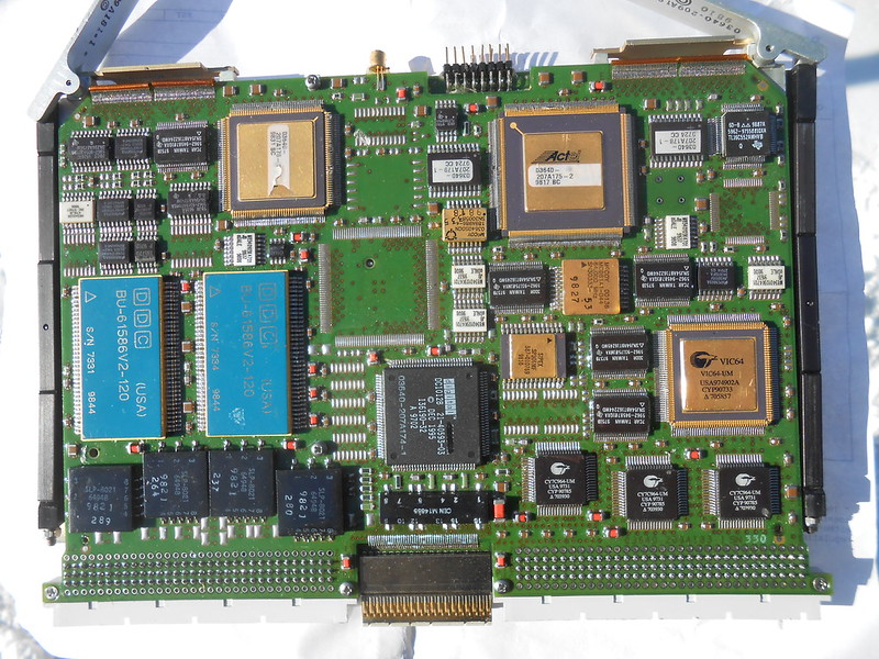

When that upside-down daughterboard in the 2nd photo is removed, we can see underneath it:
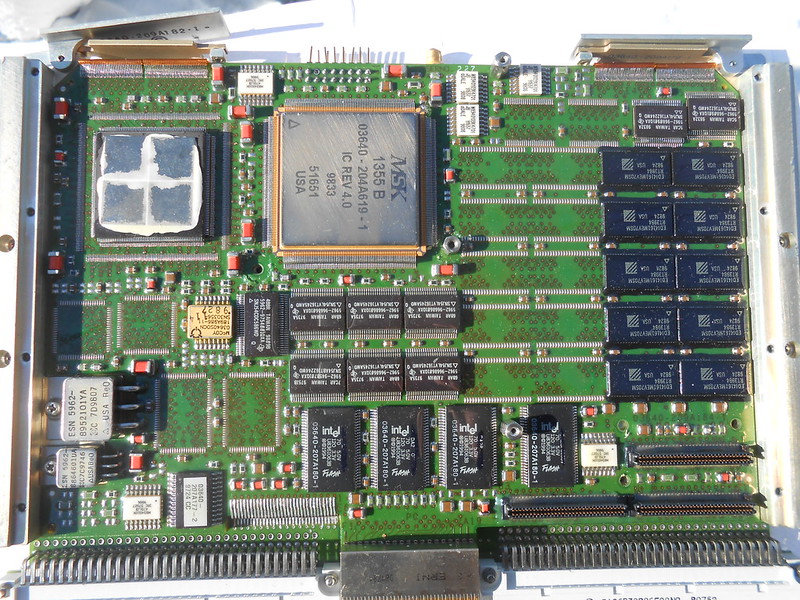
...and can take a look at the daughterboard too:


The "03640" that appears repeatedly is the CAGE code for IBM Federal Systems Division (now Lockheed-Martin), the makers of a
much older series of aerospace computers used in the space shuttle and elsewhere. This board is much newer, though: the date codes are all around 1997, which makes it roughly 30 years old. As for the particular model, I came across
a post where a particularly-knowledgeable Claude Methot tracked it down to the SP-103 single-board computer, and provided a link to
an example of a later model, the SP-103B. (The text "SP-103" also appears on the levers used to remove it from a card cage, which confirms this.)
This would be one of many boards in a
"VME crate", controlling others via VMEbus. Other VME boards in the "crate" might be specialized I/O (such as waveform digitizers or generators), or other computers.
Reverse engineering: finding part numbersAs with most "Lego-block style" digital devices, the reverse-engineering doesn't go very deep here, but we can at least look up all the IC part numbers to get an idea of what it does. Most of the parts are easy to read, but there's a couple outliers.
The large chip here, with metal plates glued to it for heatsinking, turns out to be the CPU:

Removing the metal & glue (not shown here) reveals it as the Thomson-CSF TSPC603E, a 32-bit PowerPC part. Judging by the manufacturer, a big player in military avionics, this is presumably a fairly rugged part made to work across a wider temperature range than a "commercial-grade" PowerPC CPU.
This big MS Kennedy module with the custom part number is also a mystery: it's probably a complicated hybrid module with lots of bare dies and laser-trimmed resistors inside, right? Right?

Not quite.

It turns out to be just a footprint-adapter/interposer for a Motorola XPC106A "northbridge" chip. The XPC106A interfaces the PowerPC's native data bus to both external memory, and a PCI bus for all the peripherals.
I strongly suspect that this (painfully expensive) custom adapter was made because of thermal expansion coefficients. Different materials expand or shrink by different amounts as the temperature changes, and not always in a simple linear way. This is a major consideration in the packaging of electronic components, where mismatch between the thermal expansion of a component, and the circuit board it's soldered to, creates stress in the hard (and therefore brittle) solder joint. Repeated temperature cycling causes metal fatigue, and eventually this can crack the solder joint if something else hasn't failed first. This is even more of an issue in military & aerospace electronics, where the components have to endure both a much wider temperature range, and larger/faster temperature changes.
The XPC106A was probably only available in this
BGA package. BGAs are more sensitive to thermal mismatches, since the mechanical & electrical connection is through many rigid balls of solder. An array of solder balls like this has very little "give": a small strain will translate to a large stress. So, by mounting the XPC106A BGA here to the purple ceramic substrate, the ceramic XPC106A package and its substrate have similar thermal expansion properties and will not put excessive stress on the BGA's solder balls as the temperature changes.
The connections from the ceramic substrate to the PCB are subject to much more thermal
strain, as FR-4 fiberglass has very different thermal expansion characteristics than common ceramic materials. However, this connection is through the long, thin pins that you can see soldered to the PCB. If you know some basic Euler beam theory (or have an intuitive understanding of material behavior from experience), you'll know that these pins can bend over much larger distances than the BGA's solder balls, while creating comparatively little stress in the pins. Therefore, this custom adapter removes excessive thermal-expansion stress that might be caused by soldering the BGA package directly to the PCB, while still putting some power-filter decoupling capacitors nice and close to it.
Reverse engineering: overviewNow, looking at all the parts, we can see that this does look like a general-purpose single-board computer, which could've been used for any number of things:


One thing which stands out is the number of different I/O interfaces:
- 2x dual DDC MIL-STD-1553 modules = 4x MIL-STD-1553 channels
- 10x RS-422 transmit channels & 18x receive channels, when the daughterboard is included; some of these may be discrete signals (via the TL16C552's parallel port), while some may be serial channels (via the TL16C552's dual UART interfaces)
- Wired Ethernet
- Optional SCSI, through a chip which isn't populated on these boards (but was in other copies I saw for sale)
Let's go on a photo tour of the other features:
PowerThe two all-metal power packages are linear regulators: one of these likely provide lower core voltages (such as 1.8V or 2.5V) for the CPU. The original VMEbus standard only supplies +5V for the digital logic - the VME64 standard includes +3.3V too, but this is from 1994 and so might've been too new at the time this board was designed. The VIC64 (VMEbus interface controller) and the TL16C552 (serial & parallel ports) run from +5V, but most of the other ICs require +3.3V. So, one of these regulators might be supplying +3.3V to the whole board, if the VMEbus doesn't provide it.

They'll dissipate a lot of power, considering how much current all the complex digital ICs draw, but that's what the direct mounting to the conduction-cooled base plate is for.
Front-to-back connectionsIn case it wasn't clear already, this whole assembly consists of two PCBs mounted on each side of a metal plate. These two PCBs are connected together with some polyimide flex cables soldered in a few places:

The daughterboard has only one PCB, but it's mounted to a particularly-thick stiffener/heatsink. Instead of a solid plate on the non-component side of the PCB, this stiffener is a honeycomb-style array of "compartments":
 VMEbus interface ICs
The
VIC64 handles the protocol used on the VMEbus (bus arbitration, buffering data until it can be sent, etc.).

It can drive 8 of the data & address lines directly, but for the rest, external transceivers are needed. The 3x
CY7C964 transceivers cover 8 bits each of the address and data bus, for 32 bits each of address & data. These have with high-current drivers for outputs, and an address comparator so they can signal the VIC64 when another device wants to talk to this board.
 Ethernet interface
The
21040 Ethernet controllers are made by DEC - you can see both them and the transformers used for the wired Ethernet interface here.

Strangely, the packages have a number crossed out with a marker, and the custom IBM/Lockheed part number (starting with 03640) stamped on them separately. These must deviate from the standard parts in some way, probably by taking the standard commercial parts and screening them with extra environmental testing (such as temperature-cycling, burn-in, or ionizing radiation) to bring them up to IBM's "military-spec" requirements.
I can imagine some unfortunate technician though just sitting there with a marker and a stamp, modifying the markings by hand on hundreds of chips.
Resistor arraysEach of the white ceramic packages is a resistor array:

With so many identical resistors, they probably have something to do with the data bus(es). The particular ones in that photo look like 4.7KΩ, so that suggests a bus pull-up or pull-down (to keep it in a defined state when all drivers are off), rather than some small series-termination resistances.
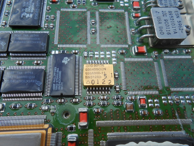
OscillatorsThere are a few different crystal oscillators spread throughout. I can't tell what each one is for, although I'd assume the CPU and Ethernet controller each have their own oscillator.

 Memory
Permanent storage (4M x 16 = 2M x 32, or 8MB) comes in the form of these Intel flash chips:
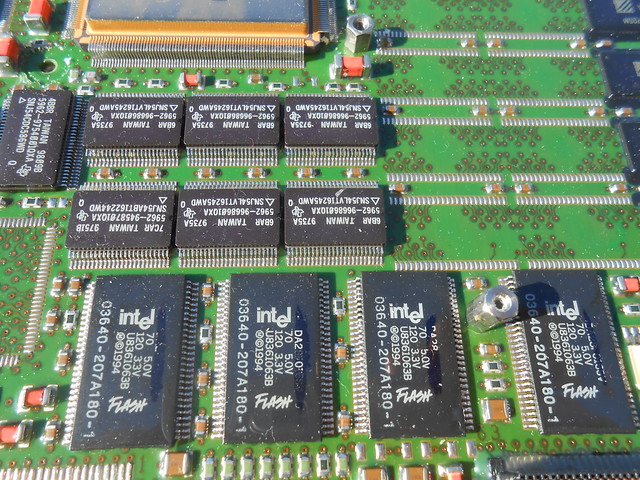
Like the Ethernet controller, all of these also seem to have pen marks crossing out the 'standard' part number, and a custom IBM part number stamped on. Again, these are probably commercial parts that have been up-screened in some way.
The RAM (DRAM, 10M x 16 = 5M x 32, or 20MB) lives nearby. These parts are made by EDI
(see datasheet link here), which advertises them specifically as a "ruggedized" plastic package - I don't know exactly what that involves.

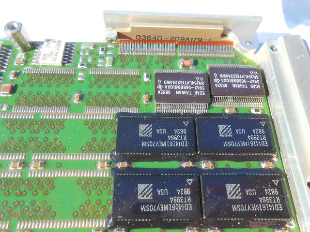
Here's another view of all the wide buffer/bus-transceiver chips it takes to interface to the memory:

There's also lots of room for extra RAM:
 Empty footprints
There's a lot of extra features that aren't populated. I'm not sure what goes in all of these:


 Differential transceivers
This board has no shortage of differential I/O, as listed above. It comes in a few different varieties - from the RS-422/RS-485 ICs in one corner...

...to a Sipex dual-Rx/dual-Tx RS-422 IC in the middle of things...

...and finishing with the set of different RS-422 transceivers lurking on the daughterboard:


The purpose of all these channels is unclear. Some might be individual, discrete I/O signals (either part of some specific interface, or just general-purpose), while some might be used for serial communications (such as with RS-422 or RS-485).
The
TL16C552 in the corner has two UARTs, and a parallel port. At least some of the differential I/O are probably connected to this chip.

The other chips that potentially use the differential transceivers are the...
FPGAsThere are 3 Actel FPGAs: 2 near the peripherals, and 1 on the daughterboard with extra differential transceivers.


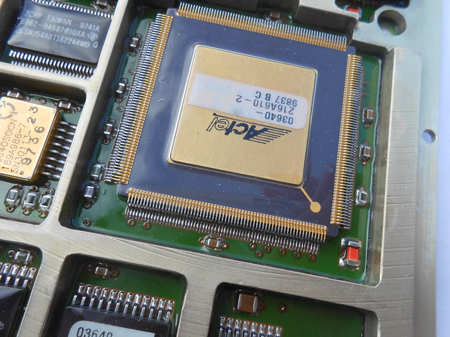
I can see 3 possibilities for how these FPGAs are used:
- Specialized I/O peripherals for some kind of communication that uses differential transceiver channels (especially with the daughterboard)
- Glue logic to interface the PCI bus (from the XPC106A northbridge) to the peripherals which expect more traditional address/data/read-and-write signals
- Uncommitted, for use by the application software as hardware acceleration
Any combination of these seems plausible. Let me know if you have ideas or additional thoughts.
MIL-STD-1553 transceiversThe modules with blue lids are
MIL-STD-1553 serial bus interfaces. Let's open one up:


These contain both a physical-layer interface (high-current drivers, and input receivers/comparators), and dedicated logic to handle the MIL-STD-1553 protocol so that this task can be offloaded from the main CPU. The largest bare die above holds this digital processing logic, with two large memory areas as well. The yellow bare die is also memory, likely message buffers to store messages from the CPU or received on the serial bus. I wasn't able to get good images of these under the microscope due to the board's size & shape, and the large die sizes.
However, we can take a closer look at the physical layer. This module is a
dual MIL-STD-1553 interface, and as a result you can see 2 identical copies of a smaller die, and smaller sub-substrates with resistors and diodes. This smaller die is a DDC custom transmitter/receiver:


A couple big power transistors are obvious at bottom-center, which are the transmit drivers. If you're curious what the analog circuitry looks like for transmitting & receiving '1553 signals, you can go read about the schematic-level reverse-engineering I did on some other '1553-PHY hybrid modules
here and
here.
There's also a 74HC04 6x-logic-inverter in this module, to show what a more modern CMOS process looks like compared to the 70's & 80's ICs I usually show:


 Home
Home Help
Help Search
 Login
Login Register


