Sometimes it is desirable to make different dopings visible. Often the goal is to read the content of a ROM. Many ROM implementations are directly visible: for example, when data is stored by placing or omitting contacts. Another method is to leave the thick field oxide under a gate electrode instead of forming a gate oxide. Variations of active areas in the substrate are also visible. However, the data stored in an implant ROM remain invisible at first glance. In such ROMs, memory cells differ only by whether a local doping was introduced or not.
Different dopings are not easily visible. In older processes and larger structures, the regions can often be recognized because different oxide thicknesses form above them during manufacturing. These layers show different interference colors, indirectly revealing the doping. If the upper layers of an integrated circuit must be removed to expose the ROM, the doping differences are usually no longer recognizable. Even with the upper layers intact, dopings are not always visible.
There are several ways to make different dopings visible. In theory, doping changes the reflection of infrared light, but this is at least difficult perhaps impossible to apply to small structures. Electron microscopy can analyze doping extensively, but the effort is considerable. The most common method is the so‑called dash etch, using a mixture of hydrofluoric acid, nitric acid, and acetic acid. Nitric acid oxidizes the silicon, hydrofluoric acid dissolves the oxide, and acetic acid regulates the reaction. With the right mixture, differently doped regions etch at slightly different rates. n‑doped areas are etched slightly deeper than p‑doped areas, and the height difference can be seen optically. Darkfield illumination is recommended.
A lesser‑known and simpler method is the application of silver fluoride. Silicon does not react directly with silver fluoride, but it causes silver ions to be reduced and metallic silver to deposit. Different dopings lead to different reduction strengths.
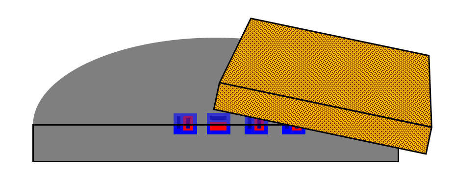
In the semiconductor industry of the former GDR, silver fluoride was used to analyze doping profiles. The integrated circuits shown here were first ground at an angle of 8,5°. This increases the visible width of the layers by a factor of 6,7, making analysis easier.
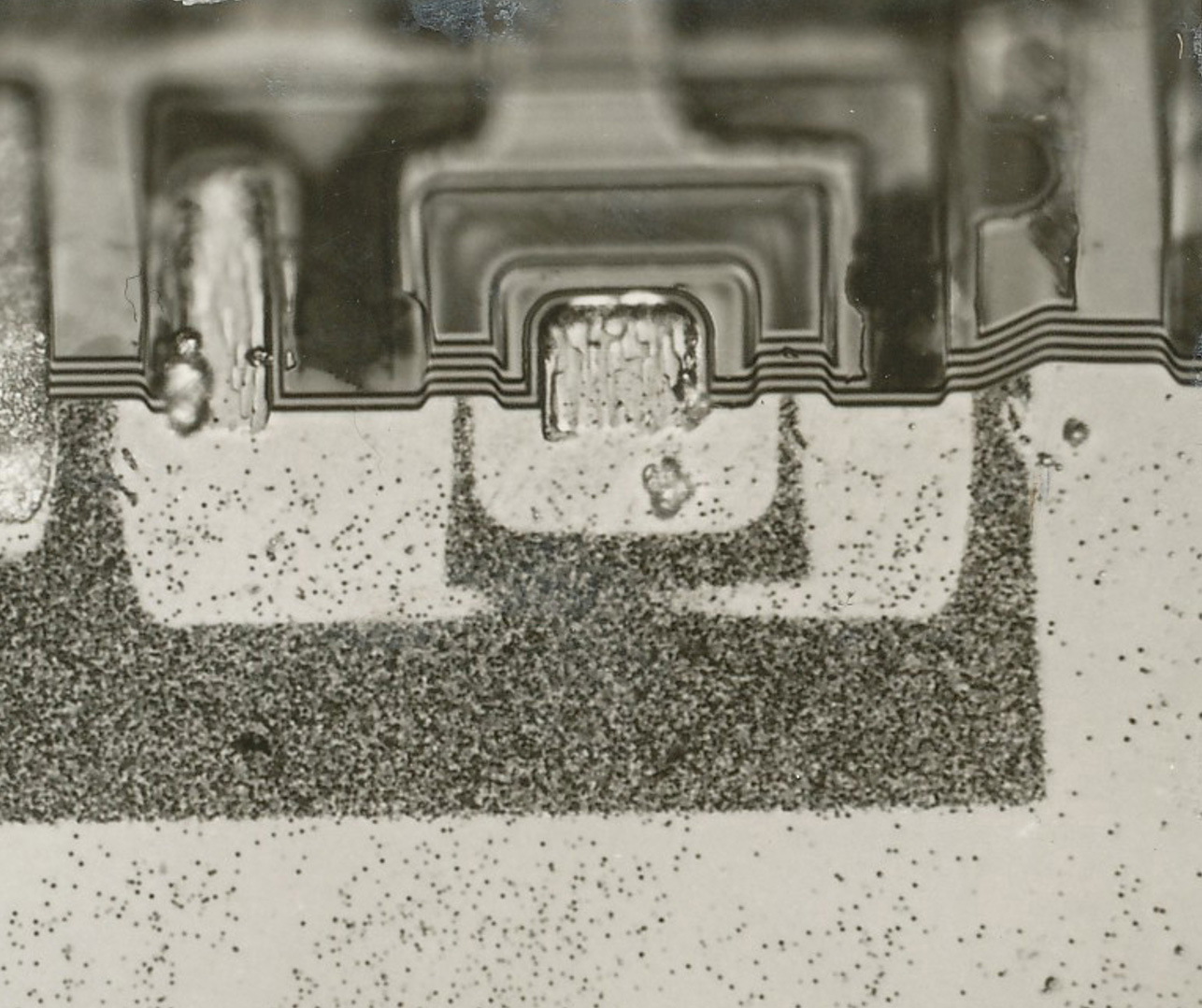
Silver fluoride was then applied to the ground edge, revealing the different dopings.
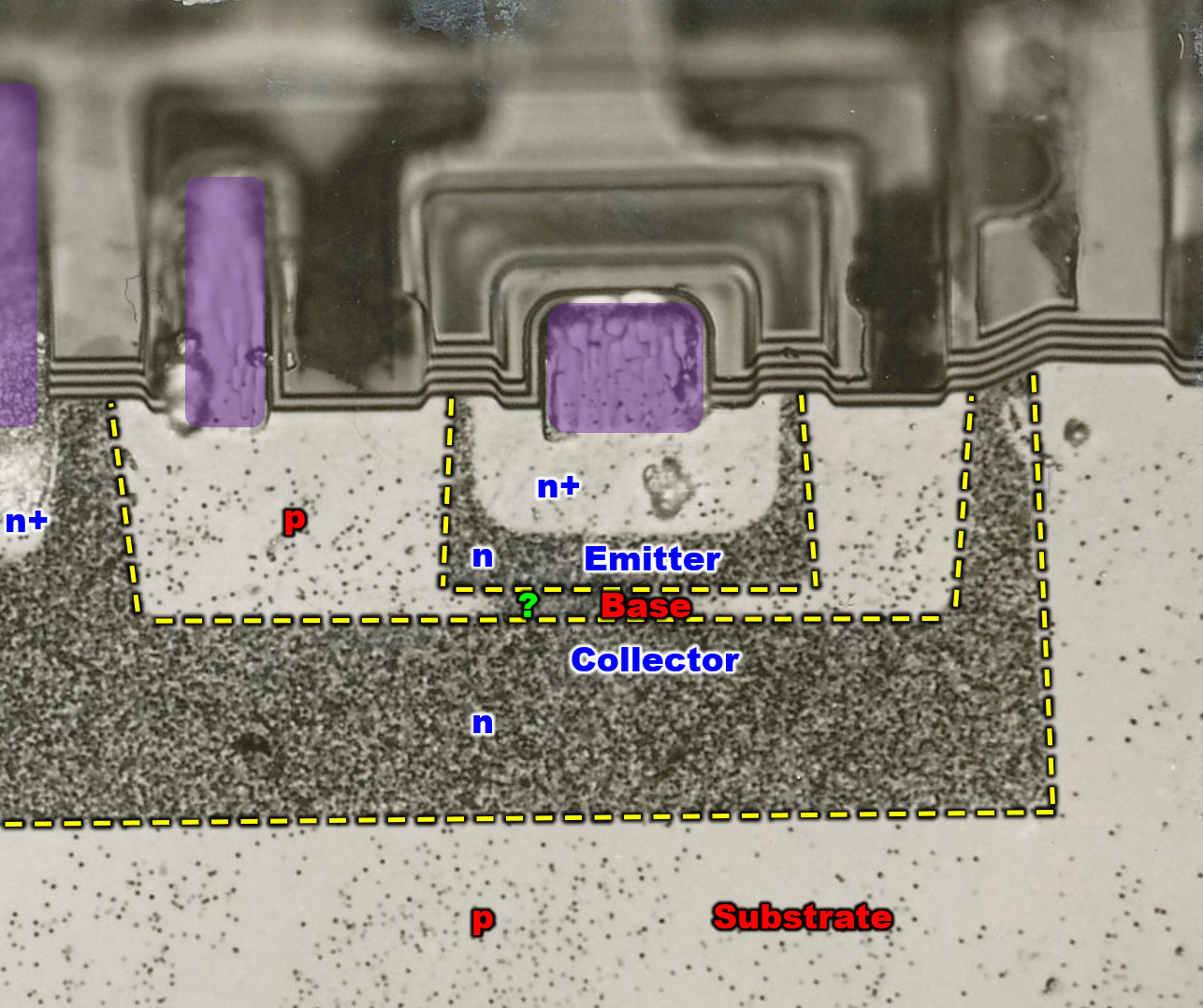
The polished cross‑section shows many interesting relationships. Based on the remaining surface structure, the arrangement of contacts, and the doping profiles, one can conclude that this is an NPN transistor. The collector contact is on the left, partly outside the image. In the center is the square emitter contact. Between collector and emitter lies the base contact.
More silver has deposited on the n‑doped regions, making them appear darker. Surprisingly, the heavily n‑doped regions used for ohmic contacts appear as bright as the p‑doped areas.
The widening collector well shows how the doping spread during manufacturing. The correctness of the doping assignment is confirmed by the angles of the wells: p‑doping diffuses significantly faster than n‑doping, causing n‑doped wells to shrink during processing.
At one point, emitter and collector appear to touch. If this is not an artifact, the emitter diffused too far into the silicon — a critical parameter for any bipolar transistor. The base width should be small, but emitter‑collector contact makes the transistor unusable.
On the surface are several thin layers, likely silicon oxides formed during processing. The high number of layers above the emitter seems unusual, since the emitter is introduced last.
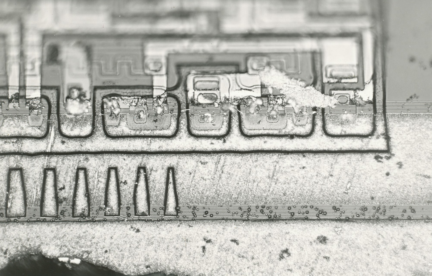
This IC is a Soviet 256‑bit memory built in I²L technology. A special feature is the large silicon‑oxide tub in which the transistors sit in small isolated wells. Manufacturing such structures is complex. The underside of the tub was originally the top of the wafer. After forming the oxide tub, a thick silicon layer was grown on top. The wafer was then flipped and ground from the original backside until the oxide tubs were reached. From there, transistor fabrication continued. In the documentation of the TP1322 you can see how such a process can look like (
https://www.richis-lab.de/Opamp49.htm).
Unusual are the deep trenches on the underside of the silicon. Electrically they likely have no function — perhaps they were relevant during manufacturing. Aligning the wafer after flipping is apparently not trivial.

Silver fluoride can be purchased as a solution normally used by dentists for treating caries. As a medical product it is expensive, but only small amounts are needed. Silver fluoride is corrosive and leaves persistent dark stains.
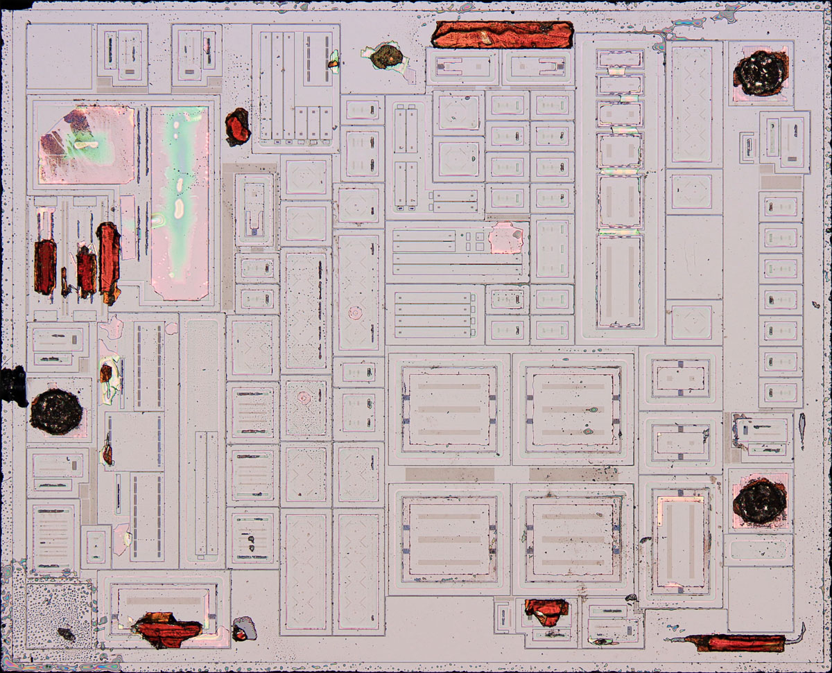
The NEC µPC811 opamp is manufactured with a relatively modern process (
https://www.richis-lab.de/OpampA17.htm). After removing the upper layers, the differently doped regions are only faintly visible.
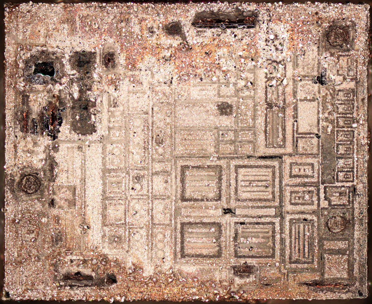
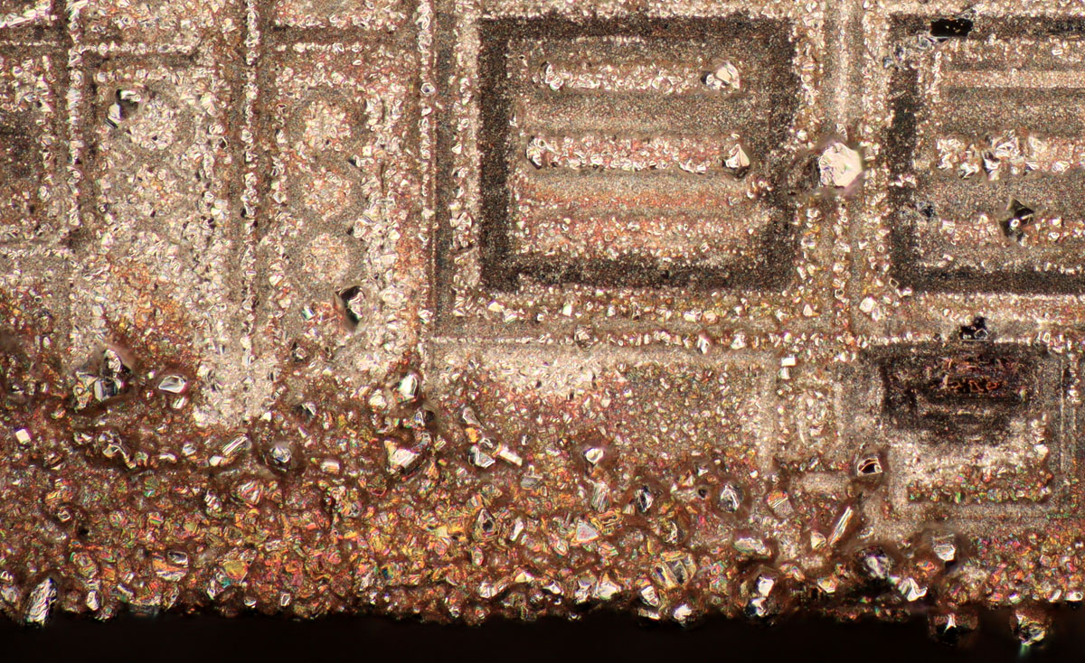
Applying a drop of silver fluoride solution and letting it act for one minute deposits a thick silver layer. Nevertheless, some selectivity is already visible.
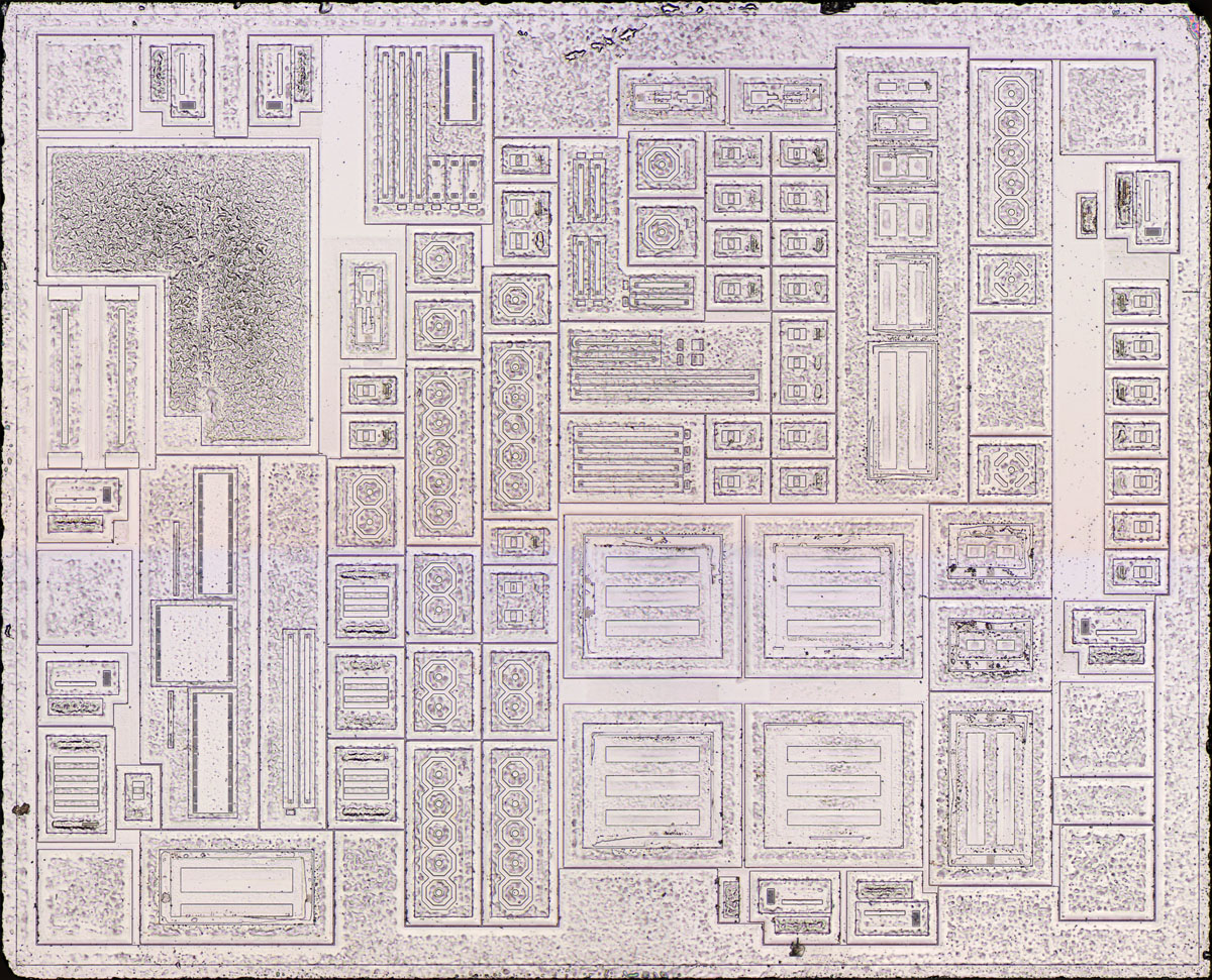
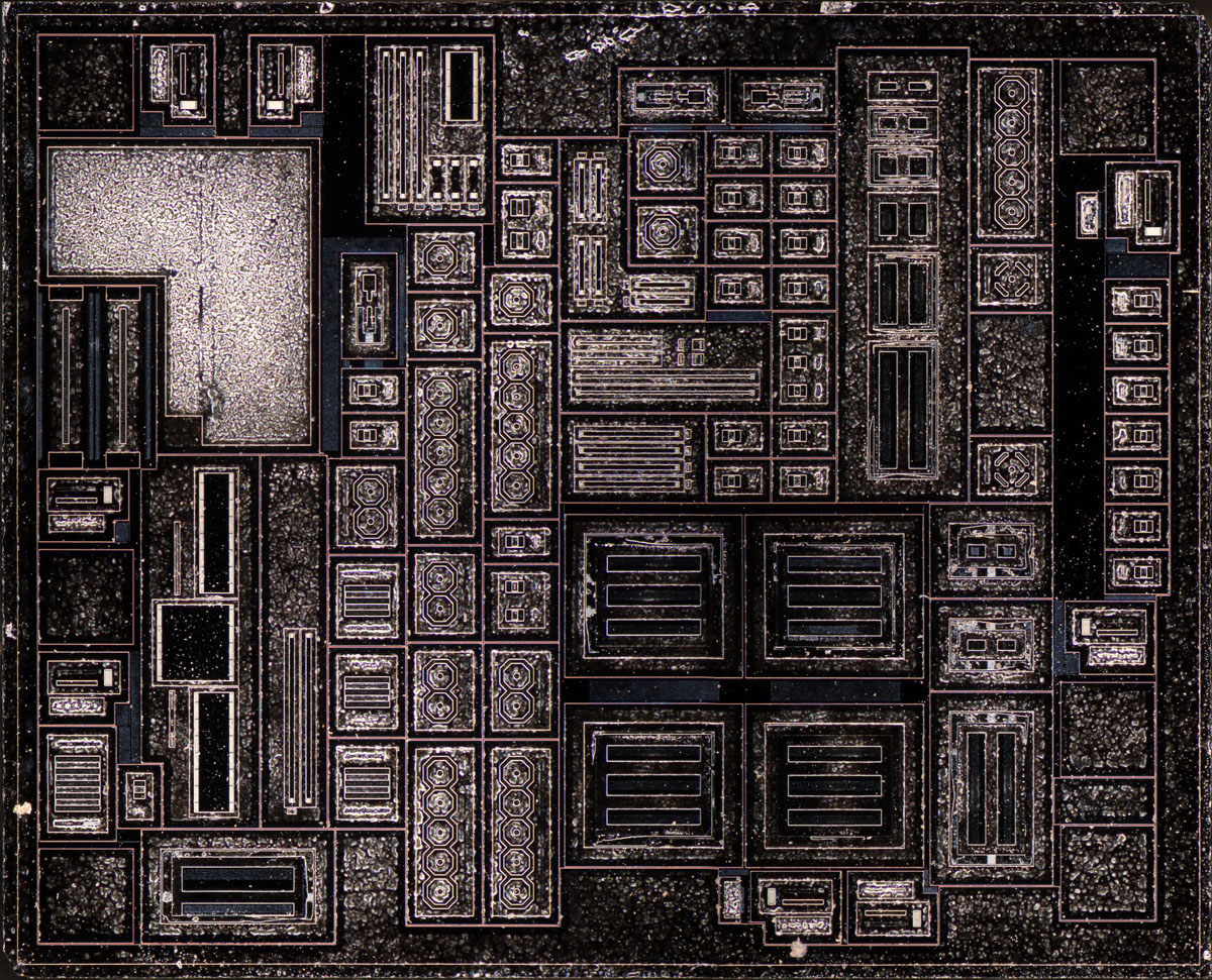
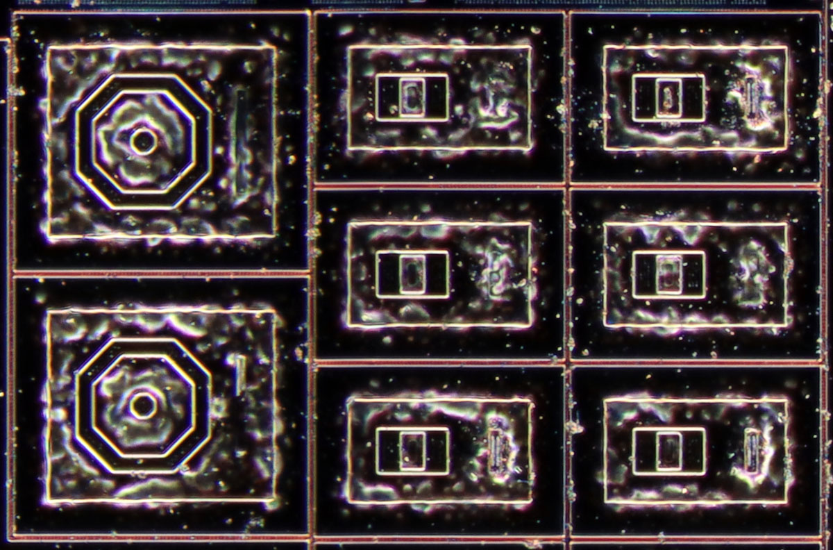
With only 10 seconds exposure, much less silver is deposited. Selectivity is again visible, but the silver particles are relatively coarse. Another 10 seconds already produce a thick layer that hides more than it reveals.
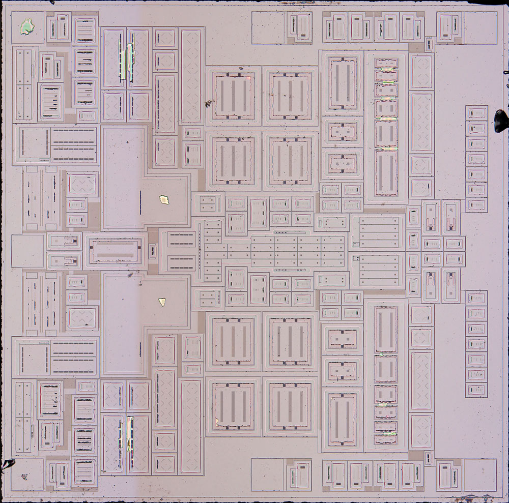
The µPC812 is the dual‑opamp version of the µPC811.
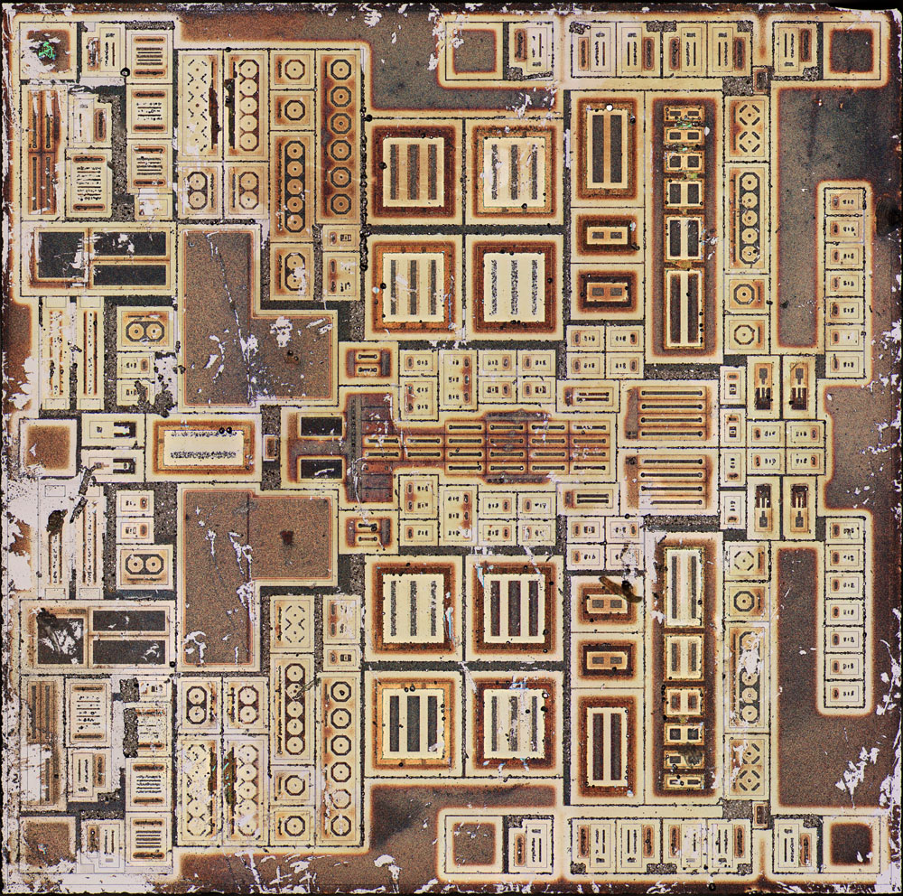
Diluting one drop of silver fluoride solution with 1ml of water produces much finer silver deposition. Since silver does not bond to silicon, the layer is very delicate. The solution must be rinsed off with isopropanol, but the surface must not be mechanically cleaned — even a soft touch removes the silver completely.
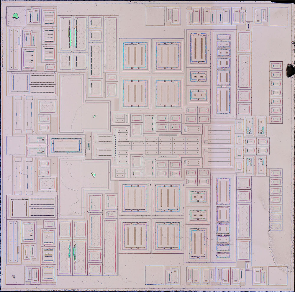
The sensitivity of the silver layer is also an advantage: if the deposition quality is unsatisfactory, it is easy to return to the starting point.
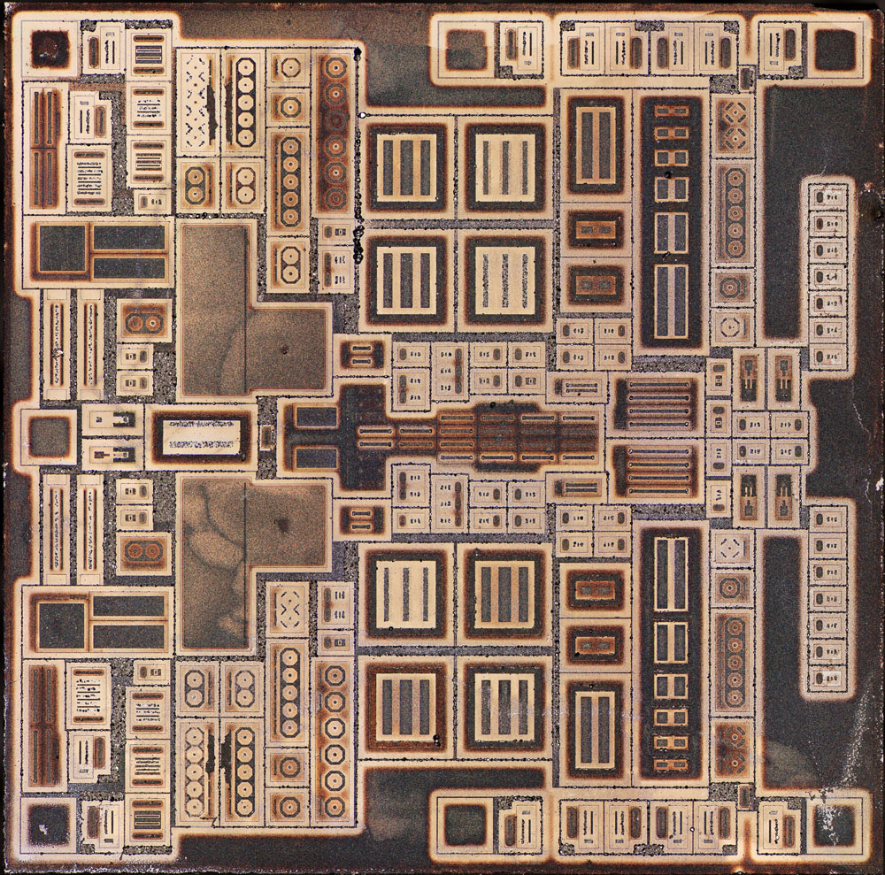
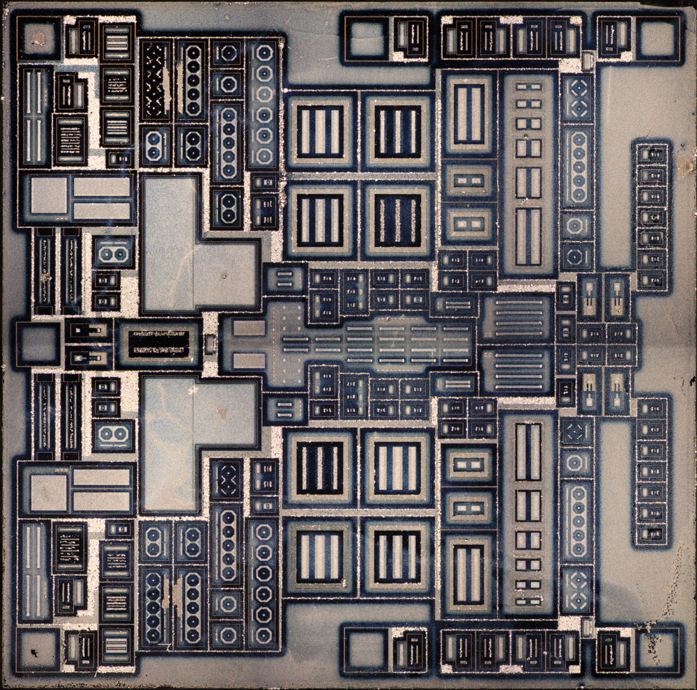
For this image, the diluted solution reacted for 5 minutes with the die.
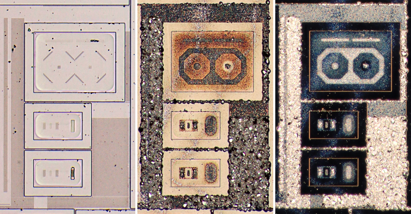
Both brightfield and darkfield images show interesting details that were not or barely visible on the untreated substrate.
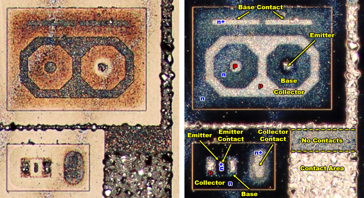
The wide stripe on the right shows strong silver deposition on contacts. The isolation frames, likely highly doped, also show heavy deposition.
The upper element contains two PNP transistors — clearly recognizable from the geometry. In the n‑doped area, little silver has deposited. More silver is found in the p‑doped regions and again on the heavily n‑doped ohmic base contact. A larger silver crystal seems to have formed on the right emitter contact. Around this crystal, less silver has deposited. Larger deposits sometimes influence their surroundings so that there is deposited less silver independend of the doping.
In the lower area, an NPN transistor is integrated. Again, the n‑doped collector region remains mostly free of silver, while the heavily n‑doped collector contact shows strong deposition. The rectangular contact inside the oval doping is visible. On the p‑doped base region, more silver is deposited than on the collector region. The contacts are visible. The emitter contact carries a larger amount of silver, but the emitter region itself is relatively free of silver — either due to the silver on the contact or because the emitter doping is lower than the collector contact doping.
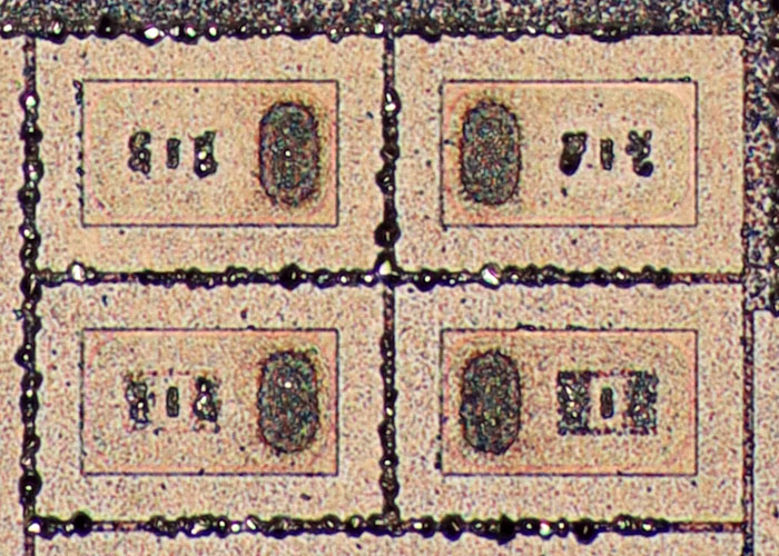
For small structures, results vary. While the lower right transistor is clearly visible, the base region of the upper transistors is missing. Larger silver deposits have formed on the contacts. Better results may be possible if the upper layers are removed more thoroughly.
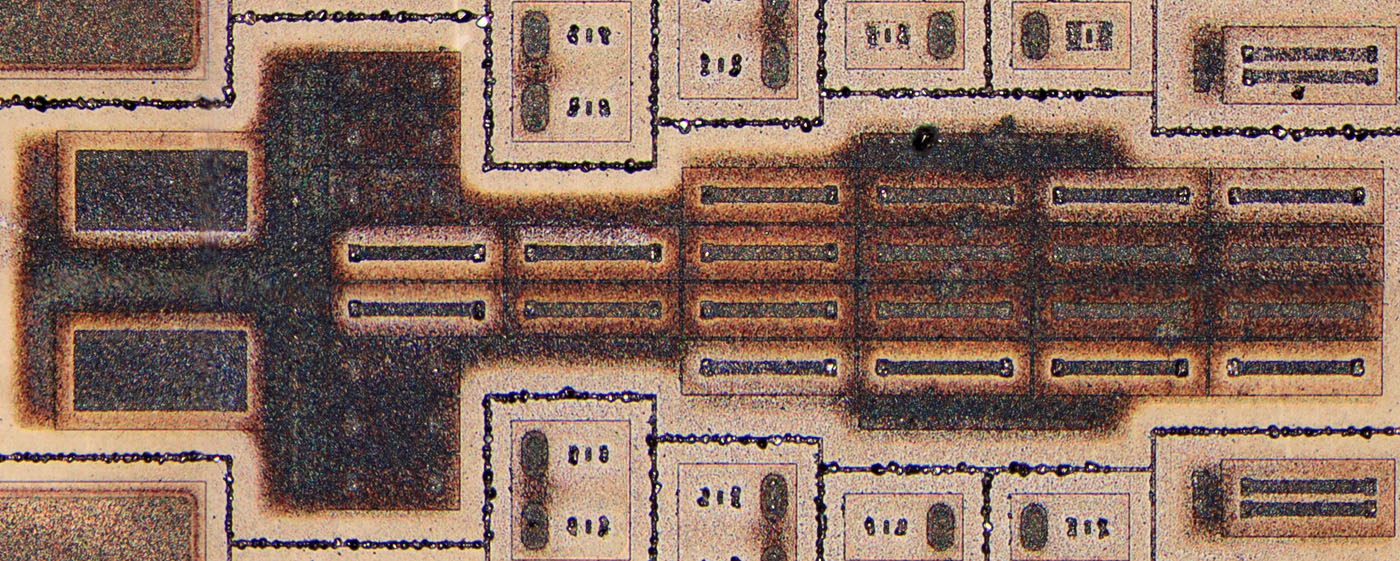
In some areas, the exposure time was already too long. Structures increasingly disappear under a uniform silver layer.
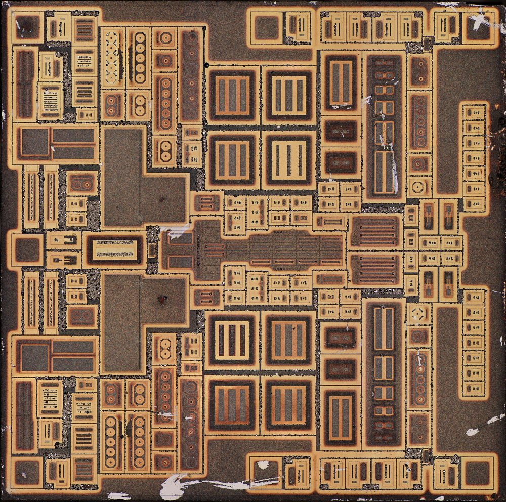
After cleaning and 8 minutes in the diluted solution, the overall result becomes worse. More structures disappear than new ones appear.
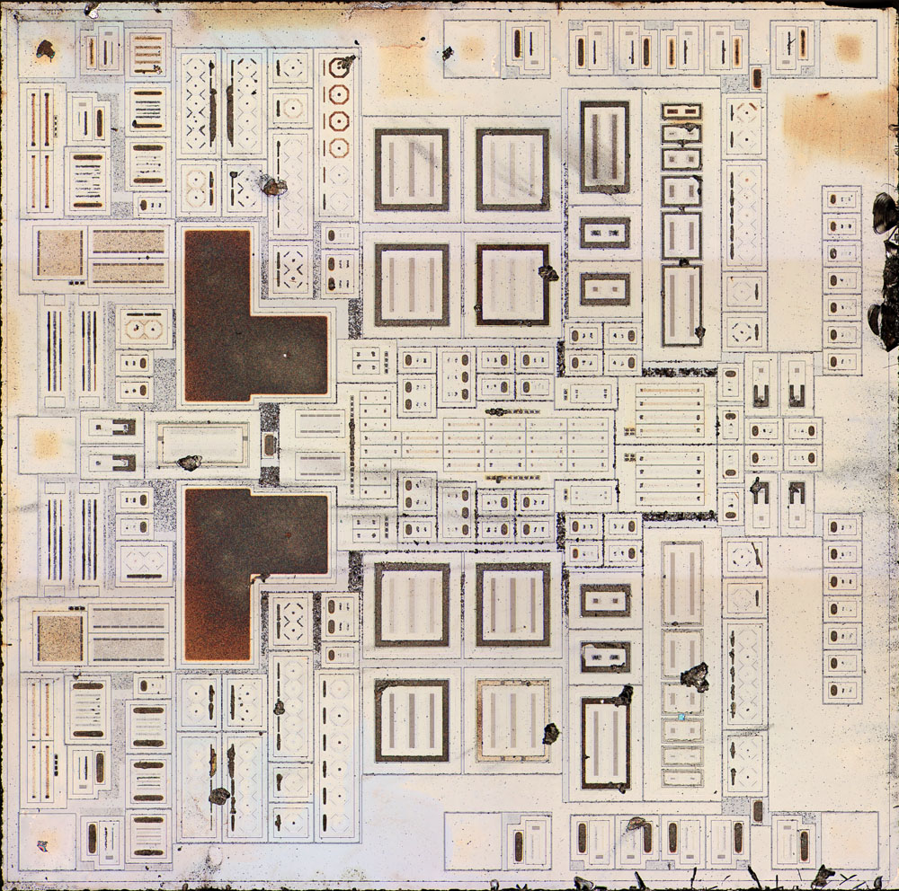
Further reducing the concentration yields poorer results. Here, one drop was diluted in 2 ml of water and the exposure time extended to 20 minutes. Silver deposits form, sometimes larger crystals, but no uniform layer appears that would allow reliable identification of dopings.
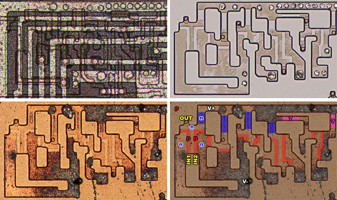
Silver fluoride can also be used to analyze MOS circuits. The excerpt above is from the Z8400 (
https://www.richis-lab.de/uC20.htm). On the substrate level (upper right), one can still see where gate electrodes were located, where polysilicon contacted active areas, and where contacts connected metal to active regions. The minimum channel length is 3,5µm.
For the image at the bottom left, the die was placed in a diluted silver fluoride solution for 8 minutes. Here, too, you can clearly see how heavily the silver deposits on irregularities. Where remnants of the metal contacts are present, very dark layers and silver crystals form. The locations of the gate electrodes were already visible before, but upon closer inspection, it is now possible to partially distinguish where the enhancement-mode and depletion-mode MOSFETs are located. Beneath the gate electrodes of the depletion-mode MOSFETs, a slightly more inhomogeneous layer of silver has deposited.
The Z8400 is based on what is known as depletion-load NMOS logic. Unlike CMOS logic, this architecture uses only NMOS transistors. The active regions are n-doped areas within a p-doped substrate. Where a MOSFET is to be formed later, there are p-doped interruptions over which the gate electrodes (red) will later be deposited. However, to build a gate, in addition to these more common enhancement-mode NMOS transistors, a structure is also needed that can provide a defined high level. The simplest solution is to use a pull-up resistor. It is significantly more efficient, however, to use a depletion-mode NMOS transistor (blue) instead. If the gate and source of these transistors are connected, the transistor behaves like a switchable pull-up resistor.
A depletion-mode NMOS transistor can be fabricated by introducing an n-type dopant beneath the gate electrode. This altered doping becomes visible with silver fluoride, as slightly more silver precipitates there. On the far right of the image, no additional doping (pink) is visible. However, the transistors there should also be depletion-NMOS transistors. This is likely due to the weakness of the method already observed above. Directly above the gate regions, there are large amounts of silver that influence deposition in the immediate vicinity.
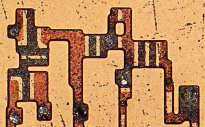
Another peculiarity is visible here: if only a narrow strip of active area lies between two gates, silver sometimes deposits much more strongly. The reason is unclear.
https://www.richis-lab.de/Howto_Decap_AgF.htm 

 Home
Home Help
Help Search
 Login
Login Register


