Author Topic: Different die pictures  (Read 212177 times)

0 Members and 5 Guests are viewing this topic.

Offline NoopyTopic starter

  • Super Contributor
  • ***
  • Posts: 2404
  • Country: de
    • Richis-Lab
Re: Different die pictures
« Reply #500 on: May 15, 2026, 10:47:34 am »
That means I was lucky to wait only one year? >:D :-DD

I have parts which are way older!  ;D
...but I always say: Tell me if it is urgent and tell me again a few weeks later.
Some parts are still interesting even two years later. This flexibility helps me maitain efficiency. Publishing a new part every 2-3 days, all year long, is dificult to to maitain as a one-man operation.

Offline NoopyTopic starter

  • Super Contributor
  • ***
  • Posts: 2404
  • Country: de
    • Richis-Lab
Re: Different die pictures
« Reply #501 on: May 21, 2026, 02:58:26 am »

...


I have taken a closer look at the ROM of the EA7044. It consists of 29 columns and 88 rows. The column select lines are located at the bottom edge. The first three address lines, with their inverted potentials, form the typical structures. The fourth and fifth address lines continue this pattern. However, their geometries have been slightly modified to save space.

In the memory area, a line with a fixed potential (yellow) is always surrounded by two data lines (green). The data lines are connected to a high-impedance potential (purple) at the left edge. The programming determines whether a gate oxide region is located above the green-yellow line pairs. With a gate oxide, the potential of a column can conductively connect the lines. As a result, it is no longer the purple potential but the yellow potential that is transmitted to the right.

Column selection uses three address lines with their respective inverted potentials. In this way, one column is selected from eight columns. The data interface is thus 11 Bit wide. Virtually, this results in a 232 x 11 Bit ROM.


https://www.richis-lab.de/calc18.htm#mem

 :-/O
 
The following users thanked this post: RoGeorge

Online Renate

  • Super Contributor
  • ***
  • Posts: 1749
  • Country: de
    • Renate's Android Page
Re: Different die pictures
« Reply #502 on: May 21, 2026, 05:24:00 am »
Hmm, this got me thinking about addressing.
Of course for RAM you can shuffle the rows and columns as you like.
With ROM you can too, but it complicates the data layout.
Have you ever seen anybody using Gray code for layout?
That would give you the benefit of reducing the zigzaginess of the address zero and one fanout by a factor of two.
Not that that seems to be a problem.


Offline NoopyTopic starter

  • Super Contributor
  • ***
  • Posts: 2404
  • Country: de
    • Richis-Lab
Re: Different die pictures
« Reply #503 on: May 22, 2026, 03:04:10 am »
Hm, no, I don´t think I have seen a Gray code adressing.
But that´s an interesting idea...

Offline NoopyTopic starter

  • Super Contributor
  • ***
  • Posts: 2404
  • Country: de
    • Richis-Lab
Re: Different die pictures
« Reply #504 on: June 08, 2026, 03:11:57 am »


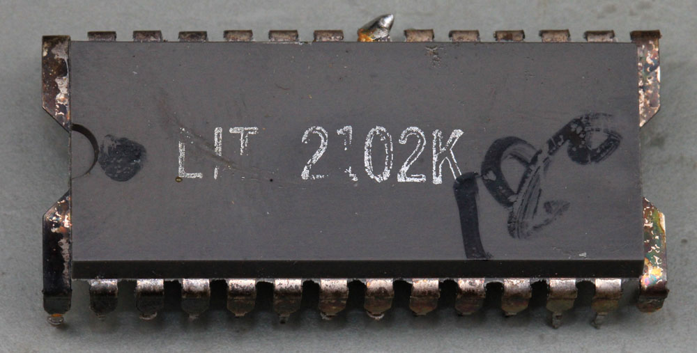
The LIT-2102 is a calculator controller manufactured by the American company Litronix. The package material resembles a gray compound that is more reminiscent of hard silicone than epoxy.
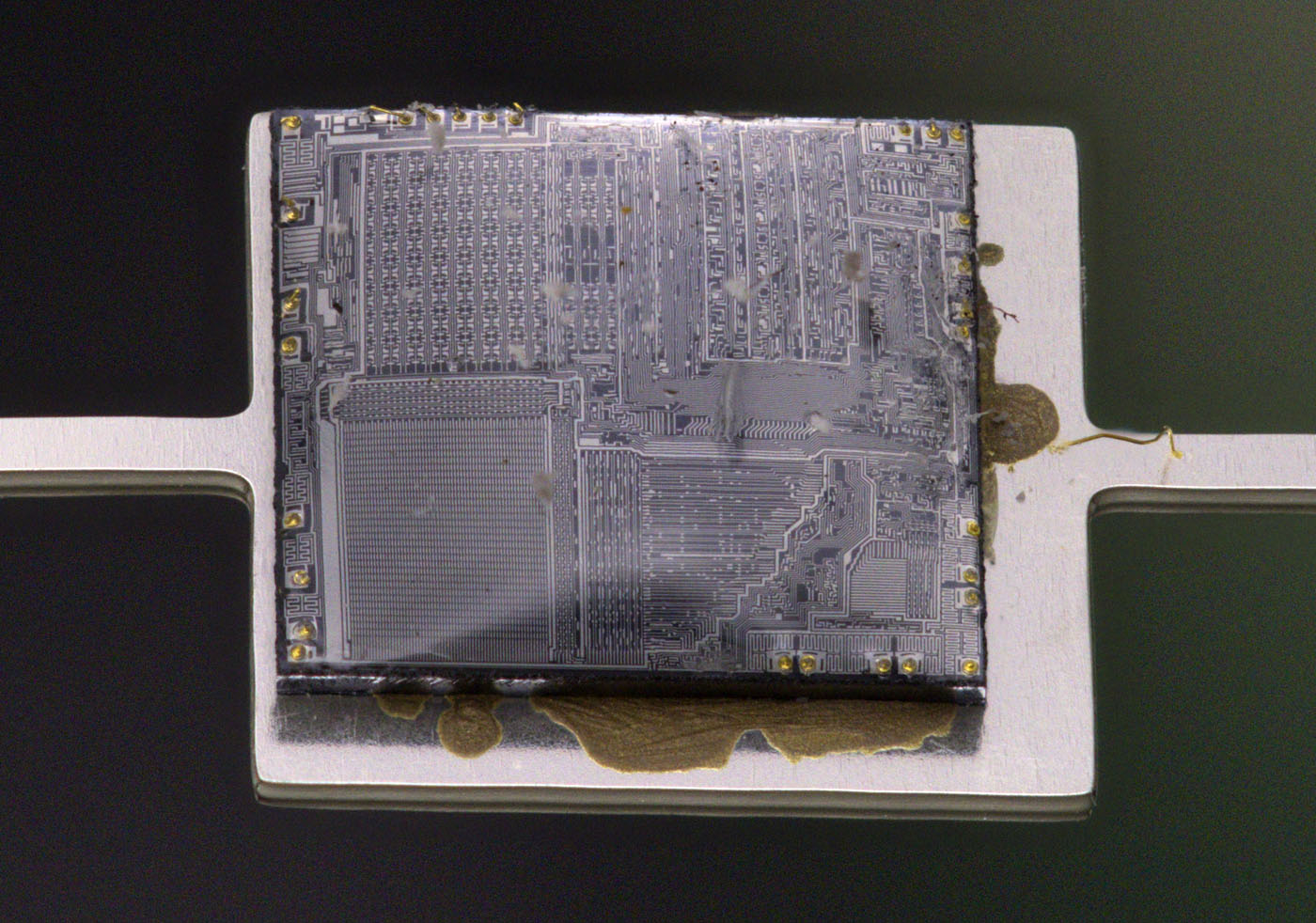


A silicone potting protects the die.
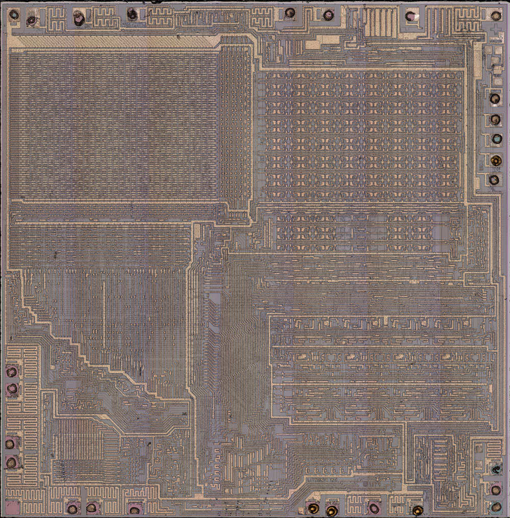


The LIT-2102 contains a die measuring 4,6mm x 4,7mm.

This image is also available in a higher resolution: https://www.richis-lab.de/images/calc/23x03XL.jpg (185MB)
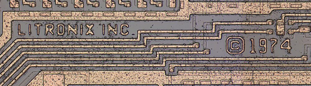


The design appears to be built by Litronix, dating back to 1974.
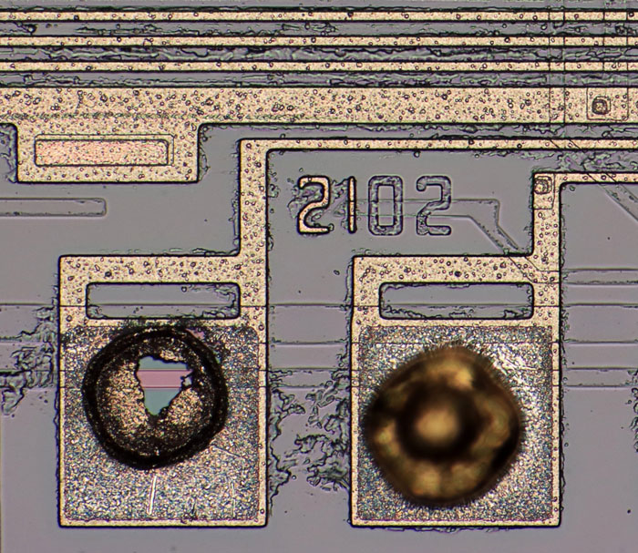


The number sequence 2102 and its placement in two levels suggest that there is an overarching basic design for the LIT-2100 family and that the LIT-2102 is a variant of it. The lower mask defines the different functionality. This mask determines either where contacts are formed or where a gate oxide should be located.
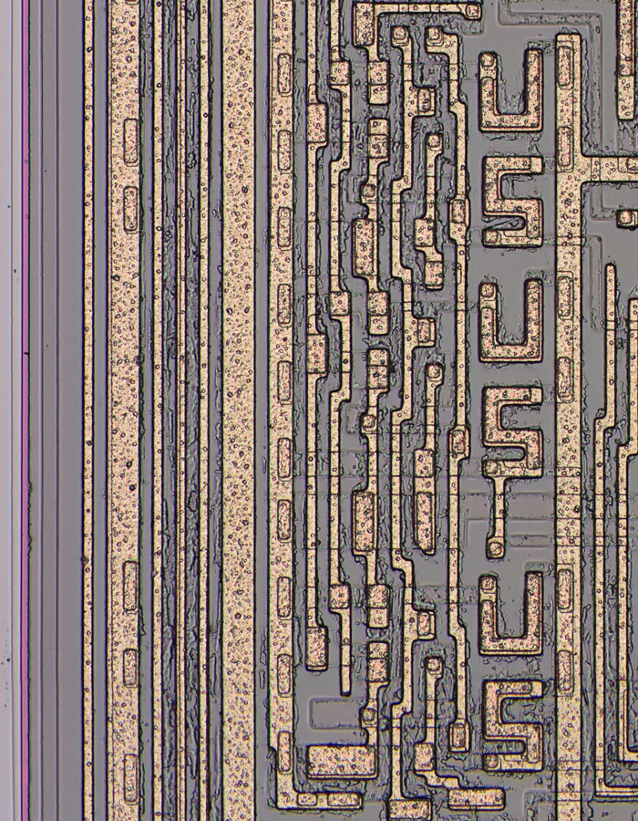


On the right edge, the letters “US” appear to have been placed one below the other three times. The letters are not immediately recognizable, partly because they are integrated into the circuit as functional components.
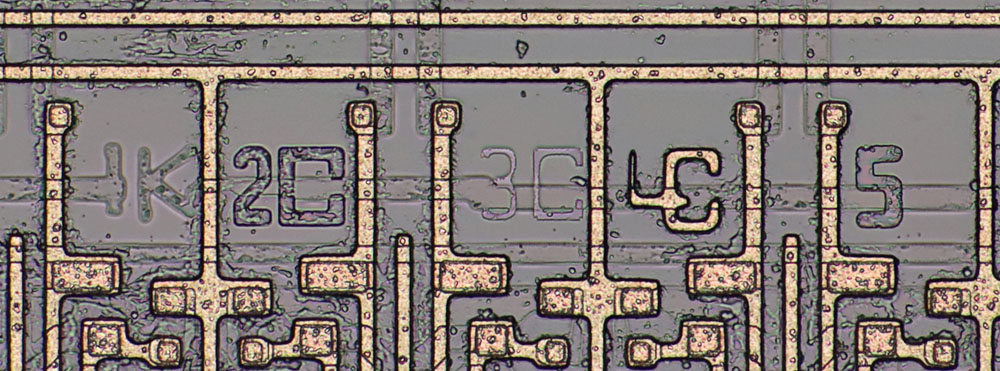


The revisions of five masks are shown to the left of the RAM area. The characters 4C have been joined together to save space.
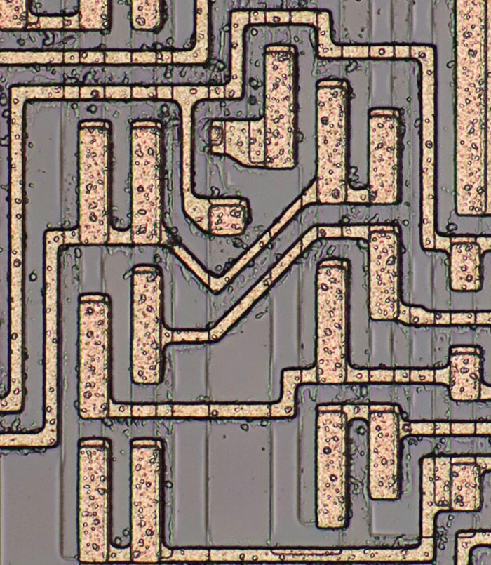


In the lower section of the die, it was clearly a struggle to route the traces.
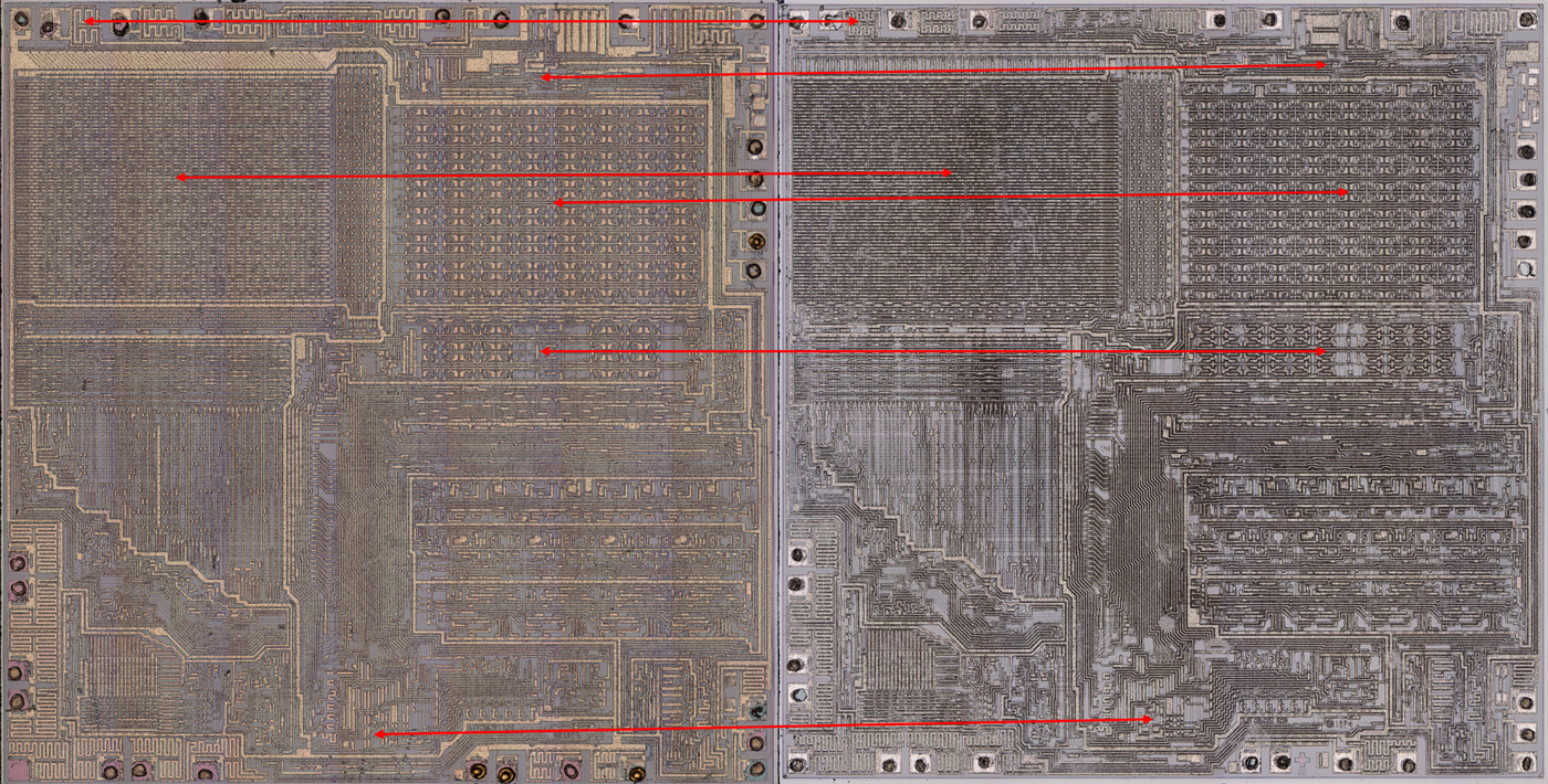


The LIT-2102 is very similar to the LIT-2314 (https://www.richis-lab.de/calc14.htm). Upon closer inspection, however, a few differences become apparent (list is not exhaustive):

The space required for the output stages at the bond pads has been slightly reduced compared to the LIT-2314. The circuitry in the upper right area has changed significantly. In the case of the ROM (upper left), not only has the surrounding circuitry changed, but also the memory depth. The LIT-2102 has 64x64 memory cells, while the LIT-2314 operates with 96x64 memory cells. The RAM (top right) has also been modified. The memory depth differs slightly in the upper and lower sections. Circuitry components have also been changed along the lower edge.
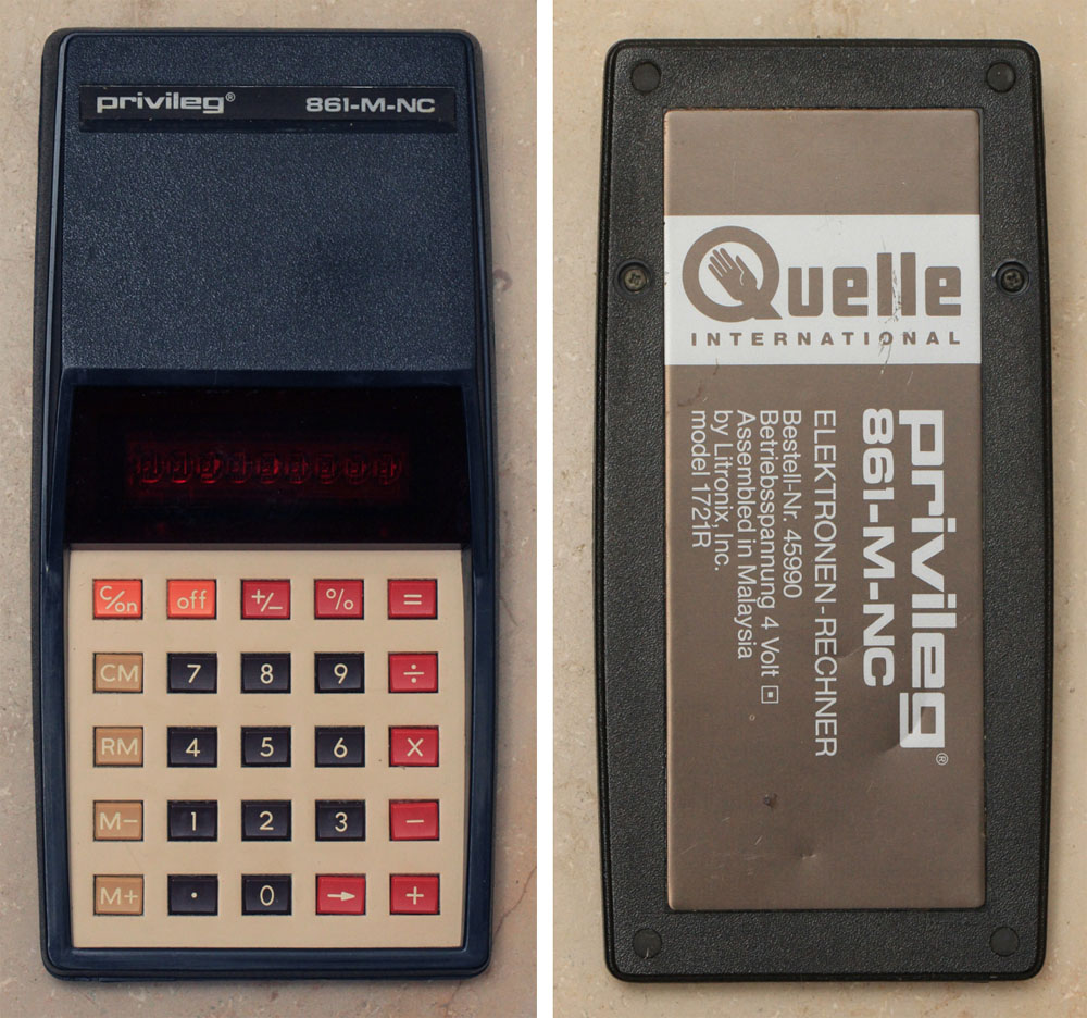


The LIT-2102 shown above was removed from the Privileg 861-M-NC calculator pictured here.
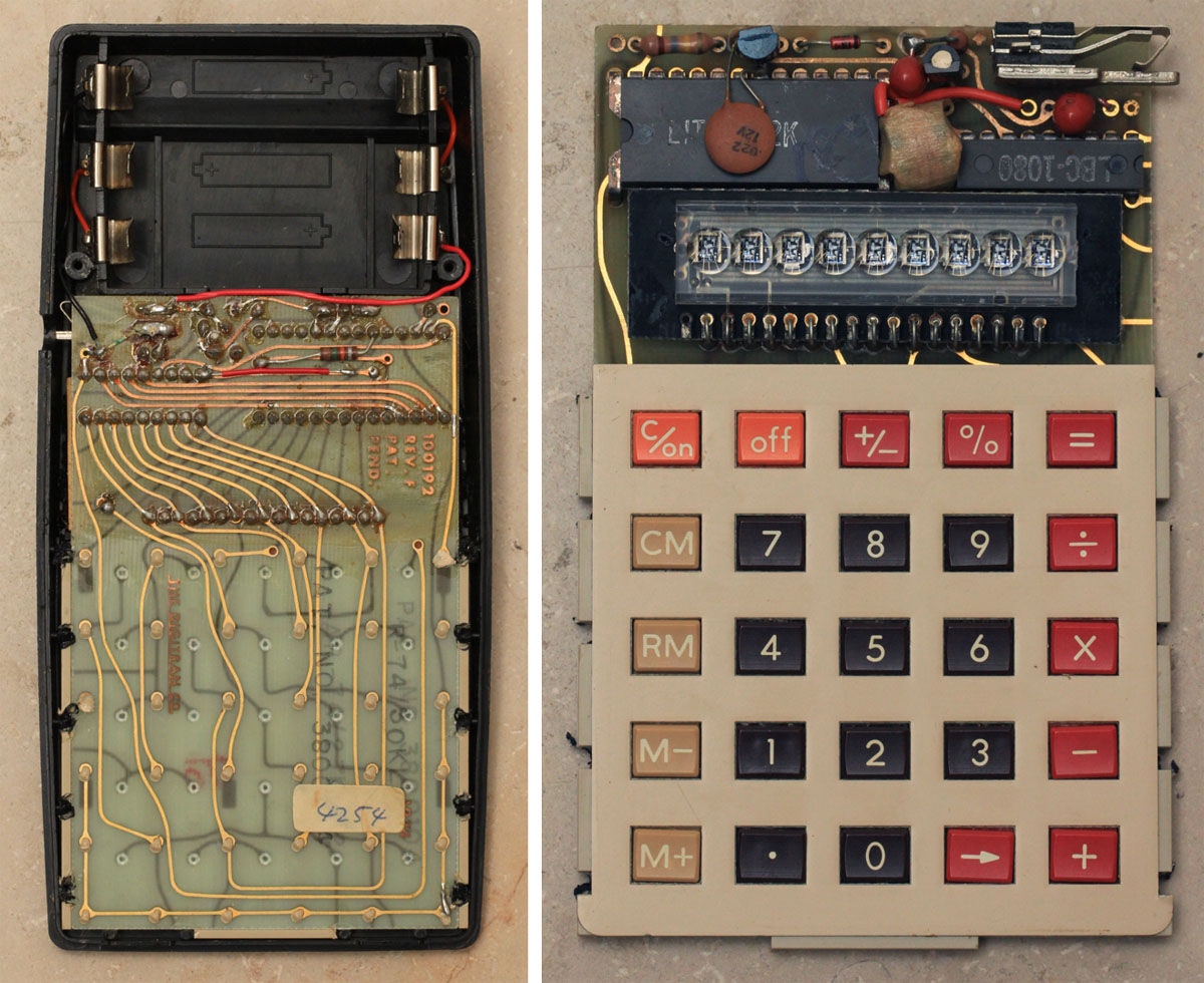


The LIT-2102 is located above the display. The LBC-1080 next to it is not just a segment driver; it is a special auxiliary component.
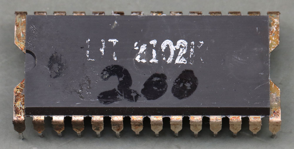


Here is a second LIT2102. Upon closer inspection, you can see an irregularity in the center of the package.
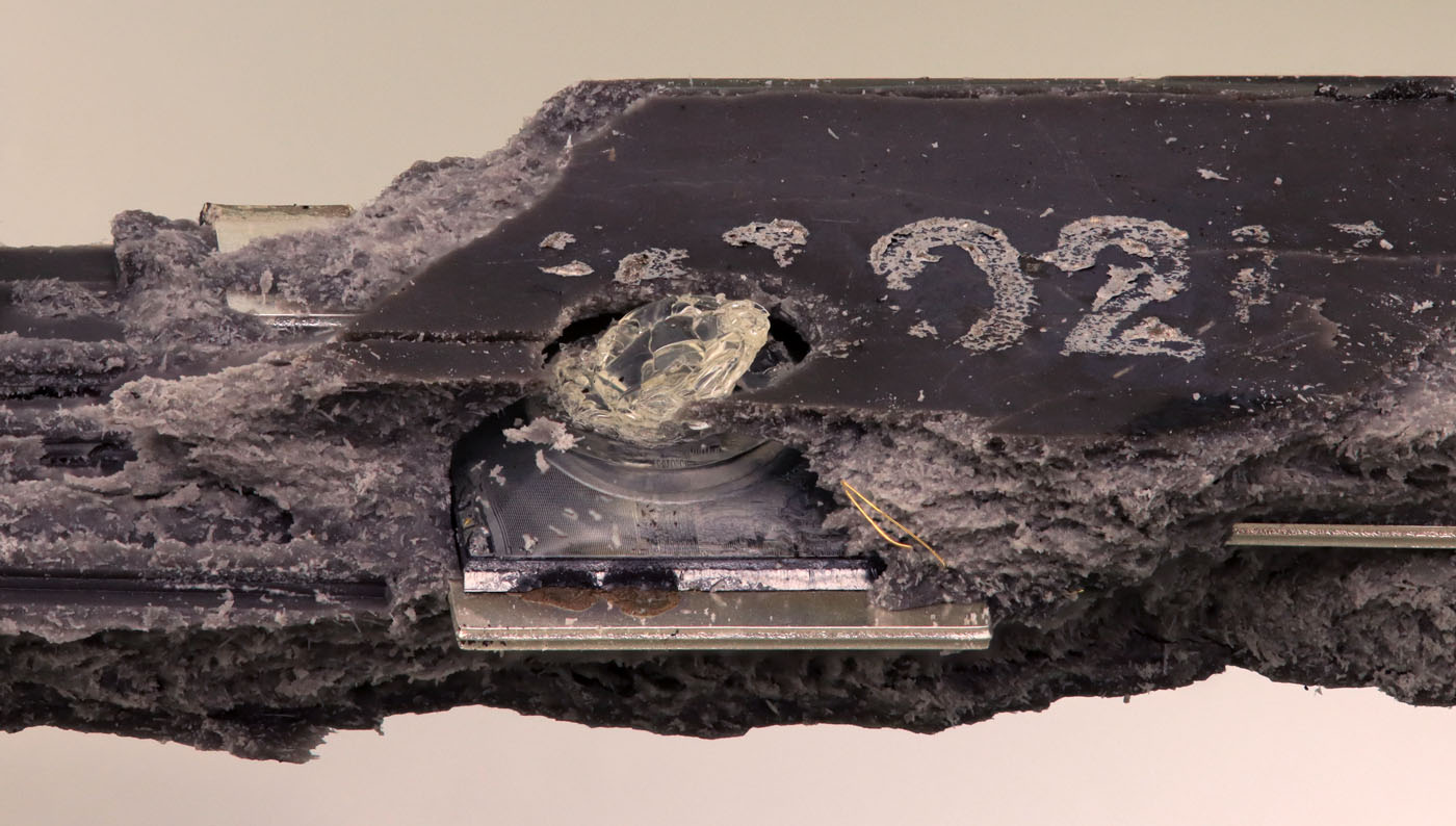
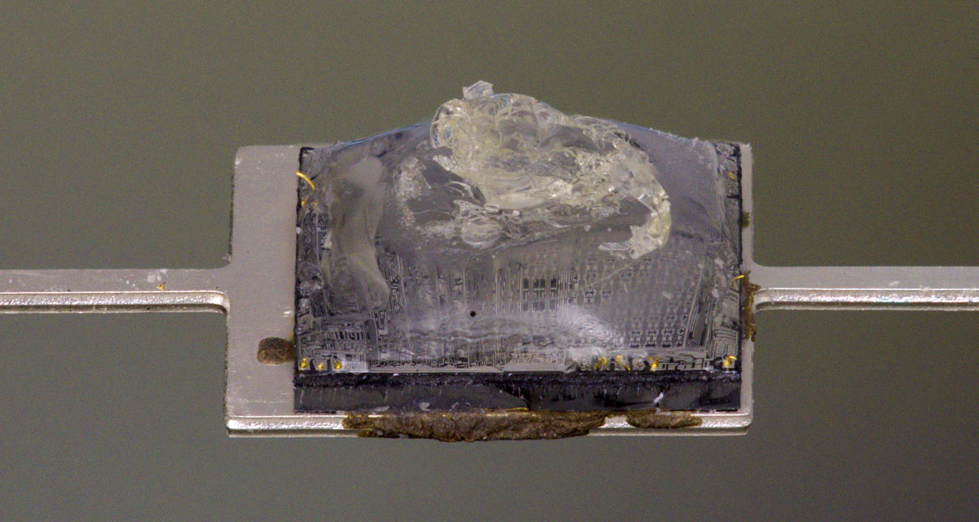


It appears that the irregularity was caused by an excessive amount of silicone. The package material was so thin at this point that it could no longer form a stable layer. From a durability standpoint, this is a major problem, as many substances can diffuse through silicone. It protects the die only from mechanical influences; the package material must provide protection against environmental influences.
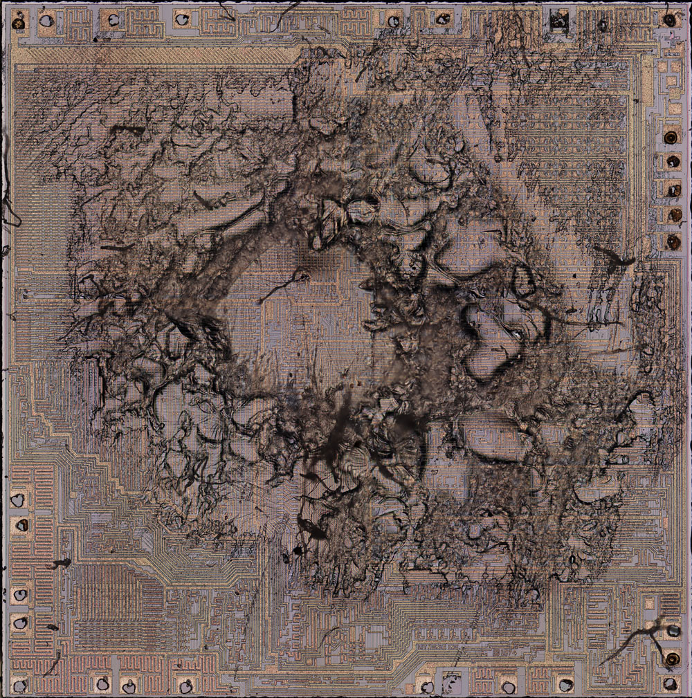


Silicone is very difficult to remove without leaving any residue. So-called silicone removers only loosen the silicone; they do not dissolve it. Silicone residue between the circuit traces is particularly stubborn.
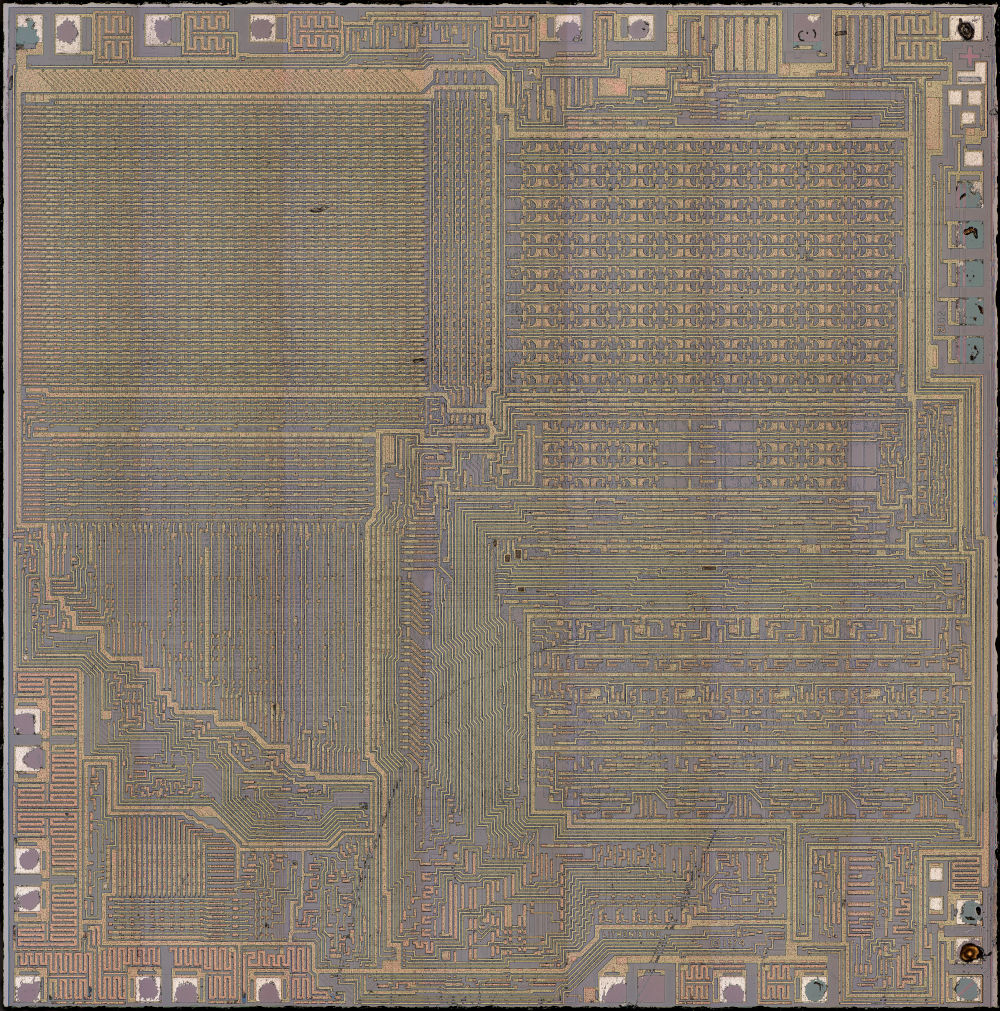


No differences can be detected between the two LIT-2102.

This image is also available in a higher resolution: https://www.richis-lab.de/images/calc/24x05XL.jpg (117MB)


https://www.richis-lab.de/calc20.htm

 :-/O
 
The following users thanked this post: RoGeorge, D Straney

Offline NoopyTopic starter

  • Super Contributor
  • ***
  • Posts: 2404
  • Country: de
    • Richis-Lab
Re: Different die pictures
« Reply #505 on: June 08, 2026, 03:13:05 am »


The Litronix LBC-1080 is a peripheral device designed for use with the LIT-2102 calculator controller.


The die measures 1,7mm x 2,0mm. It is therefore significantly larger than the die of the LBC-1082.

This image is also available in a higher resolution: https://www.richis-lab.de/images/calc/25x02XL.jpg (43MB)


Here is another LBC-1080.


This die appears to have exactly the same structure as the first die. The surface is less damaged.

This image is also available in a higher resolution: https://www.richis-lab.de/images/calc/26x02XL.jpg (42MB)


https://www.richis-lab.de/calc21.htm

 :-/O
 
The following users thanked this post: RoGeorge, D Straney

Offline NoopyTopic starter

  • Super Contributor
  • ***
  • Posts: 2404
  • Country: de
    • Richis-Lab
Re: Different die pictures
« Reply #506 on: June 16, 2026, 03:32:58 am »


The AB5301A is a microcontroller optimized for audio applications from the Chinese company Bluetrum, founded in 2016. It features a 125 MHz RISC-V processor with 1 MB of flash memory and 190 kB of RAM. In addition to a radio receiver and various audio signal channels, it also includes a Bluetooth interface.

Bluetrum microcontrollers are known for having lettering that often have nothing to do with the component designation. This is also the case here with the string CTXC14B5A. The datasheet contains no explanation of how to interpret the lettering.


There are two chips inside the package. The upper chip is the AB5301A's flash memory.


The microcontroller measures 2,3mm x 2,4mm. RF circuitry is located at the top left and bottom right. The area at the top left must represent the Bluetooth interface, as the same structures are found on the BT8922H2 (https://www.richis-lab.de/uC11.htm). The BT8922H2 appears to have a very similar layout.

This image is also available in higher resolution: https://www.richis-lab.de/images/uC/15x03XL.jpg (63MB)


The design incorporates multiple layers of metal. Nevertheless, interesting structures can be seen in some areas.

This image is also available in a higher resolution: https://www.richis-lab.de/images/uC/15x04XL.jpg (12MB)


This image is also available in a higher resolution: https://www.richis-lab.de/images/uC/15x05XL.jpg (11MB)


These inductors with their specialized geometries are commonly found in integrated circuits that process high frequencies.


The flash memory chip measures 1,2mm x 1,0mm. The markings indicate that the chip was manufactured by UCUN Technology, a Chinese company founded in 2018.

This image is also available in higher resolution: https://www.richis-lab.de/images/uC/15x08.jpg (11MB)


The top section shows the memory controller. Below that, you can see the uniform, very small structures of the memory itself.

This image is also available in a higher resolution: https://www.richis-lab.de/images/uC/15x09XL.jpg (6MB)


https://www.richis-lab.de/uC15.htm

 :-/O
 
The following users thanked this post: RoGeorge, ch_scr, D Straney, Thomas Ballantine

Offline NoopyTopic starter

  • Super Contributor
  • ***
  • Posts: 2404
  • Country: de
    • Richis-Lab
Re: Different die pictures
« Reply #507 on: June 18, 2026, 03:13:14 am »


The AB5322B is very similar to the AB5301A. It features a 125 MHz RISC-V processor with 512kB FLASH and 124kB RAM. The audio area has "less channels".


The microcontroller measures 2,0mm x 2,2mm. The IC closely resembles the AB5301A, but is slightly smaller. As said the AB5322B has fewer audio channels but particularly noticeable is the absence of the large inductor in the lower right corner.

This image is also available in a higher resolution: https://www.richis-lab.de/images/uC/16x02XL.jpg (47MB)


The FLASH memory measures 1,0mm x 0,5mm. It is a part from Puya Semiconductor designated PY1905V1.

This image is also available in a higher resolution: https://www.richis-lab.de/images/uC/16x03XL.jpg (11MB)


https://www.richis-lab.de/uC16.htm

 :-/O
 
The following users thanked this post: RoGeorge, D Straney

Offline NoopyTopic starter

  • Super Contributor
  • ***
  • Posts: 2404
  • Country: de
    • Richis-Lab
Re: Different die pictures
« Reply #508 on: June 21, 2026, 03:43:29 am »


The FR1001 is a calculator controller manufactured by the American company Frontier.


The grayish package material leaves stubborn residue on the die.


Unfortunately, the necessary mechanical cleaning leaves a few scratches, but at least the residue can be completely removed when viewed from the surface. The die measures 5,3mm x 5,5mm. The large, elongated elements on the top and right edges are shift registers. Equally noticeable are the wide, mostly horizontal metal strips, beneath which the logic’s resistors are located.

This image is also available in a higher resolution: https://www.richis-lab.de/images/calc/27x03XL.jpg (125MB)


The upper edge bears the designation FR.1001 and five symbols. ST, DC, HH, and KO could be the developers' initials.


Various test structures have been distributed across the edges. Three different MOSFETs can be seen here. The numbers .4, .5, and 4.2 indicate the gate lengths in mils (thousandths of an inch). Multiplying these by 25,4 gives the length in micrometers.


https://www.richis-lab.de/calc22.htm

 :-/O
 
The following users thanked this post: RoGeorge, ch_scr, D Straney

Offline NoopyTopic starter

  • Super Contributor
  • ***
  • Posts: 2404
  • Country: de
    • Richis-Lab
Re: Different die pictures
« Reply #509 on: June 27, 2026, 03:38:02 am »


Here is a printed sticker that has an RFID transponder on the back. The interior of the antenna structure resembles a UFO, which is reflected in its name. UFO70 is the abbreviation for the RFID-ST-U-UFO703M from the Thai company Smart Identify. The datasheet reveals that the transponder IC is an NXP UCODE 8.


The actual RFID transponder is located in the upper part of the “UFO,” on a small cut in the metallization. The two circles likely make it easier to position the small IC.


The IC itself is coated with a polyimide layer that carries two large and two smaller contacts.The datasheet states that the smaller contacts serve solely to better match the transceiver to the antenna impedance. Removing the upper layers is not easy, as the contacts stabilize the polyimide. Furthermore, it is generally difficult to mechanically process the surface of such a small die.


The die measures 0,49mm x 0,48mm.

This image is also available in a higher resolution: https://www.richis-lab.de/images/transponder/07x05XL.jpg (16MB)


A little bit better than my old picture of the UCODE 8...  ;D


The design dates back to 2018.


https://www.richis-lab.de/transponder07.htm

 :-/O
 
The following users thanked this post: RoGeorge, D Straney

Offline Ranayna

  • Super Contributor
  • ***
  • Posts: 1308
  • Country: de
Re: Different die pictures
« Reply #510 on: June 27, 2026, 01:59:52 pm »
[...]
The die measures 0,49mm x 0,48mm.
[...]
That makes me wonder: How thick are the blades of the saws used to cut the wafer into individual dies usually?
 

Offline NoopyTopic starter

  • Super Contributor
  • ***
  • Posts: 2404
  • Country: de
    • Richis-Lab
Re: Different die pictures
« Reply #511 on: June 27, 2026, 04:07:07 pm »
[...]
The die measures 0,49mm x 0,48mm.
[...]
That makes me wonder: How thick are the blades of the saws used to cut the wafer into individual dies usually?


https://www.enas.fraunhofer.de/en/departments/SP/services/dicing.html
Quote
The thickness of such a blade defines the dicing width and blades from 15 µm up to 500 µm can be used.

But today there are also these laser diving technologies:
https://www.disco.co.jp/eg/solution/library/laser/laser.html

Offline NoopyTopic starter

  • Super Contributor
  • ***
  • Posts: 2404
  • Country: de
    • Richis-Lab
Re: Different die pictures
« Reply #512 on: July 05, 2026, 04:13:28 am »


I have an update for the MCS7529!


The new picture is a little bit better.  ;D

The newer image is also available in a higher resolution: https://www.richis-lab.de/images/MCS7529/11XL.jpg (148MB)


Dunkelwind, also known as bITmASTER, who wrote an emulator for the U821 (https://www.richis-lab.de/calc01.htm), has also taken a closer look at the MCS7529 and, among other things, compiled the register architecture shown above. All of the following documents and data were also created by Dunkelwind.

This image is also available as a PDF: https://www.richis-lab.de/images/MCS7529/12.pdf


The constants available in memory are listed here.

This image is also available as a PDF https://www.richis-lab.de/images/MCS7529/13.pdf.


The shift registers are worth a closer look. The figure above, taken from the book *CMOS: Circuit Design, Layout, and Simulation* by R. Jacob Baker, shows how such a shift register is typically structured and operates. Its operation is similar to that of a so-called bucket-brigade device, as described in more detail in the context of the MN3208 (https://www.richis-lab.de/bbd02.htm). In a BBD, however, charge packets corresponding to analog signal values are constantly shifted through the register. A shift register, on the other hand, transmits only digital signals, which is why very simple buffer amplifiers can be inserted between the stages. The input capacitances of the amplifiers serve as the actual storage cells. Two phase-shifted clock signals, which must not overlap, alternately activate one or the other group of transistors arranged in a longitudinal configuration, causing the data to move through the shift register.


With the necessary background knowledge, it is easy to identify the individual elements of the shift register. The buffer amplifiers described are simply inverters, consisting of a transistor and a pull-up resistor.


Dunkelwind was also able to build an emulator for the MCS7529 that even shows how commands are processed within the program and in the logic.

The emulator can be found here: https://www.richis-lab.de/images/MCS7529/sim/index.html


https://www.richis-lab.de/MCS7529.htm

 :-/O
 
The following users thanked this post: RoGeorge, D Straney, Renate

Offline NoopyTopic starter

  • Super Contributor
  • ***
  • Posts: 2404
  • Country: de
    • Richis-Lab
Re: Different die pictures
« Reply #513 on: July 08, 2026, 03:46:35 am »


The MC14007 is a calculator controller manufactured by the Polish semiconductor company CEMI.


The die has a side length of 4,4mm. On the left side, several mask ROMs take up a large portion of the area. Equally prominent are the shift registers on the right side.

This image is also available in a higher resolution: https://www.richis-lab.de/images/calc/28x02XL.jpg (158MB)


The letters CEMI appear in the upper right corner.


In the upper-left corner, there is a sort of logo that appears to represent the letters ITE.


Five masks are shown in the lower-left corner. The test patterns make it possible to evaluate the alignment of the masks.


In the upper right corner, two characters are integrated into the metal layer. They resemble a “5B” and suggest a mask revision. Since no other mask bears such a revision mark, they could also be the letters “SB,” which might represent the initials of a developer of the IC.


https://www.richis-lab.de/calc23.htm

 :-/O
 
The following users thanked this post: D Straney

Offline NoopyTopic starter

  • Super Contributor
  • ***
  • Posts: 2404
  • Country: de
    • Richis-Lab
Re: Different die pictures
« Reply #514 on: July 11, 2026, 03:38:34 am »


The MH2103ACBT6 is a microcontroller manufactured by the Chinese company Megahunt. It is based on a ARM-Cortex-M3 core.


The datasheet directly compares the MH2103 with the STM32F103 (https://www.richis-lab.de/STM32_02.htm) and the GD32F103 (https://www.richis-lab.de/STM32_06.htm). The MH2103 is significantly faster and offers several features that the STM32F103 lacks, including encryption algorithms. The ACBT6 model refers to the smallest configuration with 128 kB of Flash and 32 kB of SRAM.


The die dimensions are 1,9mm x 1,7mm. The bondpads are arranged in two rows and offer a large number of unused options. The MH2103ACBT6 is housed in an LQFP48 package. The largest variant, the MH2103AZGT6, on the other hand, has significantly more pins in an LQFP144 package. It likely uses the same die.

This image is also available in a higher resolution: https://www.richis-lab.de/images/STM32/17_03XL.jpg (149MB)


In the lower left corner of the die, a strikingly curved font forms the letters MH 103.


Where the bondpads have been torn away, you can get an idea of how densely structured the lower layers are.


The MH2103ACBT6's flash memory is located on a second die measuring 1,0mm x 0,8mm. The actual memory area is surprisingly small compared to the control section.

This image is also available in a higher resolution: https://www.richis-lab.de/images/STM32/17_06XL.jpg (32MB)


The only markings are the letters ANDES. The letters C could represent revisions to three layers of metal.


https://www.richis-lab.de/STM32_11.htm

 :-/O
« Last Edit: July 11, 2026, 11:01:00 am by Noopy »
 
The following users thanked this post: RoGeorge, ch_scr, D Straney, Sacodepatatas

Offline NoopyTopic starter

  • Super Contributor
  • ***
  • Posts: 2404
  • Country: de
    • Richis-Lab
Re: Different die pictures
« Reply #515 on: July 13, 2026, 03:01:20 am »


The marking on this STM32F103C8T6, especially the ST logo, looks unusual. The upper-left area is particularly striking, as the characters there are barely legible.


There are two chips inside the package. It quickly becomes apparent that the microcontroller is the Megahunt MH2103ACBT6.

This image is also available in a higher resolution: https://www.richis-lab.de/images/STM32/18_03XL.jpg (151MB)


The external memory is also the same as the memory in the Megahunt MH2103ACBT6.

This image is also available in a higher resolution: https://www.richis-lab.de/images/STM32/18_04XL.jpg (32MB)


https://www.richis-lab.de/STM32_12.htm

 :-/O
 
The following users thanked this post: RoGeorge, ch_scr, D Straney, Sacodepatatas

Offline NoopyTopic starter

  • Super Contributor
  • ***
  • Posts: 2404
  • Country: de
    • Richis-Lab
Re: Different die pictures
« Reply #516 on: July 16, 2026, 03:26:19 am »


The package of this microcontroller is marked only with the characters 2514F062. Such devices are used, for example, on Blue Pill boards as an alternative to the STM32F103C8T6. Functionally, the 2514F062 is very similar to the Megahunt MH2103ACBT6.


The die measures 1,7mm x 1,5mm. The manufacturer cannot be identified. Only the letters “M475” are visible.

This image is also available in a higher resolution: https://www.richis-lab.de/images/STM32/19_02XL.jpg (34MB)


At first glance, the external memory mounted on the microcontroller appears to be the same type used in the Megahunt MH2103ACBT6.

This image is also available in a higher resolution: https://www.richis-lab.de/images/STM32/19_03XL.jpg (33MB)


https://www.richis-lab.de/STM32_13.htm

 :-/O
 
The following users thanked this post: RoGeorge, ch_scr, D Straney, Sacodepatatas

Offline NoopyTopic starter

  • Super Contributor
  • ***
  • Posts: 2404
  • Country: de
    • Richis-Lab
Re: Different die pictures
« Reply #517 on: July 16, 2026, 03:27:00 am »


At first glance, the marking on this STM32F103C8T6 doesn't look too bad.


It appears that the package contains the same microcontroller as the 2514F062.

This image is also available in a higher resolution: https://www.richis-lab.de/images/STM32/20_02XL.jpg (192MB)


The familiar external storage is also included again.

This image is also available in a higher resolution: https://www.richis-lab.de/images/STM32/20_03XL.jpg (56MB)


https://www.richis-lab.de/STM32_14.htm

 :-/O
 
The following users thanked this post: RoGeorge, ch_scr, iMo, D Straney, Sacodepatatas

Offline NoopyTopic starter

  • Super Contributor
  • ***
  • Posts: 2404
  • Country: de
    • Richis-Lab
Re: Different die pictures
« Reply #518 on: July 24, 2026, 03:21:02 am »


The AB5305B is another microcontroller optimized for audio applications from the Chinese company Bluetrum. According to the datasheet, it closely resembles the AB5301A. However, the datasheet does not provide detailed specifications for the microcontroller.

And we have another marking which doesn´t show AB5305B at all.


This die appears to correspond exactly to the die in the AB5301A. The only difference is that some different bondpads were contacted.

This image is also available in a higher resolution: https://www.richis-lab.de/images/uC/17x02XL.jpg (72MB)


Here, too, the flash memory is located on the microcontroller as a separate die. However, it is a different model than the one used in the AB5301A. Its dimensions are 1,2mm x 0,7mm. The manufacturer is Puya Semiconductor. The designation “1603” is located on the top edge.

This image is also available in a higher resolution: https://www.richis-lab.de/images/uC/17x03XL.jpg (9MB)


In detail, one can still partially make out the control of the storage area.


https://www.richis-lab.de/uC17.htm

 :-/O
 
The following users thanked this post: RoGeorge, ch_scr

Offline iMo

  • Super Contributor
  • ***
  • Posts: 6902
  • Country: li
Re: Different die pictures
« Reply #519 on: July 24, 2026, 06:42:34 am »
Quote
At first glance, the marking on this STM32F103C8T6 doesn't look too bad.
"992ka mys507" indicates a clone..
Readers discretion is advised..
 
The following users thanked this post: Noopy

Offline NoopyTopic starter

  • Super Contributor
  • ***
  • Posts: 2404
  • Country: de
    • Richis-Lab
Re: Different die pictures
« Reply #520 on: July 25, 2026, 03:30:13 am »


MOS Technology has developed two integrated circuits, the MCS2525 and the MCS2526, which were used together in scientific calculators. Very few details are available about these two chips. The MCS2525 is referred to as the master, and the MCS2526 as the slave.


The die measures 5,5mm x 4,7mm. The left side contains large ROM areas. Shift registers are located on the right. The design seems to be similar to the CEMI MC14007 (https://www.richis-lab.de/calc23.htm).

This image is also available in a higher resolution: https://www.richis-lab.de/images/calc/29x03XL.jpg (134MB)


The upper-right corner features the MOS logo, five masks, and the string “2525F.”


The mask, which appears purple, also features the character strings 2A and 001H along the left edge. The numbers 001 are also found on the package. This suggests that this is a variant or revision of the MCS2525.


Here we have the MCS2526.


The die measures 5,8mm x 4,7mm. The design is surprisingly similar to that of the MCS2525.

This image is also available in a higher resolution: https://www.richis-lab.de/images/calc/30x03XL.jpg (147MB)


On the bottom edge are the MOS logo, five masks, the character string 2526F, and 001F.


https://www.richis-lab.de/calc24.htm

https://www.richis-lab.de/calc25.htm

 :-/O
 
The following users thanked this post: RoGeorge, ch_scr, D Straney, Thomas Ballantine

Online magic

  • Super Contributor
  • ***
  • Posts: 8063
  • Country: pl
Re: Different die pictures
« Reply #521 on: July 25, 2026, 08:00:44 pm »
The die measures 5,5mm x 4,7mm. The left side contains large ROM areas. Shift registers are located on the right. The design seems to be similar to the CEMI MC14007 (https://www.richis-lab.de/calc23.htm).
Another Eastern Bloc technology copied by capitalists ;D

I searched for information about MC14007 and somebody here says that it was a substitute for MOS Technology MPS7541. This may explain similarity with other MOS calculators, particularly if "substitute" means "exact clone".
http://retrokolekcja.pl/Uklady_kalkulatorowe.php

These chips were 8-digit four-bangers with only few extra functions: square, square root, inversion, percent and memory. Found in "Brda" calculators made by Unitra-Eltra in Bydgoszcz (Brda is a river there). These calculators also had a second chip, but schematics show it as an array of buffers driving LED displays.
https://wspominajbydgoszcz.blogspot.com/2019/02/brda-w-liczbach.html

So the role of the "slave" chip in MCS252x remains unclear. Might be that it simply implements some of the additional math functions which were too complex to cram on the "master" chip.
« Last Edit: July 25, 2026, 08:06:23 pm by magic »
 
The following users thanked this post: RoGeorge, Noopy

Offline NoopyTopic starter

  • Super Contributor
  • ***
  • Posts: 2404
  • Country: de
    • Richis-Lab
Re: Different die pictures
« Reply #522 on: July 26, 2026, 04:30:07 am »
Another Eastern Bloc technology copied by capitalists ;D

 ;D


So the role of the "slave" chip in MCS252x remains unclear. Might be that it simply implements some of the additional math functions which were too complex to cram on the "master" chip.

I agree with you.
A dual-core calculator!  ;D

Offline NoopyTopic starter

  • Super Contributor
  • ***
  • Posts: 2404
  • Country: de
    • Richis-Lab
Re: Different die pictures
« Reply #523 on: July 28, 2026, 03:34:44 am »


The Intel i860 is a 64 Bit RISC processor. Intel developed this processor alongside the much better-known 32 Bit CISC processors of the x86 family. The i860 was introduced in 1989. It could be used in high-performance computers and for complex signal processing tasks. It served as a classic coprocessor, but also as a graphics processor.

The letters “XR” denote the first generation of the processor, which can operate at a clock frequency of up to 40MHz. The string “A80860XR-40” is located on the bottom of the package. The number 40 indicates the variant that supports a clock speed of 40MHz. This results in a power dissipation of up to 2,7W. Other i860 variants are only certified for up to 33,3MHz or 25MHz. At 40MHz, the performance is specified with 80MFlops.


Intel's product catalog “i750, i860, i960 Processors and Related Products” includes the block diagram of the i860XR shown above. The goal was to integrate as many functions as possible that would otherwise often require additional peripheral components. Thus, in addition to the actual RISC processor, the chip also includes a floating-point unit and a graphics processor.


The die measures 15,6mm x 10,3mm. The two cache memories, a 4 kB instruction cache and an 8 kB data cache, take up a particularly large amount of space. A total of one million transistors were used in the i860XR. The structures were manufactured using a process that Intel referred to as CHMOS IV. The feature size is 1µm.

This image is also available in a higher resolution: https://www.richis-lab.de/images/cpu/18x05XL.jpg (121MB)


What is remarkable is the large number of initials and symbols scattered throughout the die.


The design dates back to 1988. While x86 processors were typically designated 80x86, the i860 was commonly referred to by its abbreviated designation without the leading 80. Nevertheless, the full designation 80860 appears on the die.


There are a many strings on the Die that could be developers' initials. Some are simple strings, while others are full-fledged logos. A surprisingly wide variety of fonts has also been used.


CHMOS4 refers to the process used. The symbol on the dark background is probably the most complex one on the entire die.


Some characters are located beneath the metal layer.


At one point, strings were formed using contacts. The letters are slightly easier to make out if you use only one layer from the image stack.


In the lower cache block, the columns are numbered.


https://www.richis-lab.de/cpu15.htm

 :-/O
 
The following users thanked this post: RoGeorge, ch_scr, D Straney

Offline NoopyTopic starter

  • Super Contributor
  • ***
  • Posts: 2404
  • Country: de
    • Richis-Lab
Re: Different die pictures
« Reply #524 on: July 31, 2026, 03:21:05 am »


The Intel i860XP is an upgraded version of the i860XR. The clock speed has been increased to 40MHz or 50MHz. The A80860XP-50 model shown here operates at the full 50MHz. Performance increases accordingly to 100MFlops. At the same time, power dissipation rises to 5,9W. Accordingly, a heat sink has been attached to the package.


The die measures 15,9mm x 10,6mm. This makes it slightly larger than the die of the i860XR. In the i860XP, the instruction cache has been quadrupled to 16kB, and the data cache has been doubled to 16kB. This was certainly aided by the fact that the minimum feature size could be reduced from 1µm to 0,8µm. Nevertheless, the memory areas occupy significantly more area than in the i860XR. Reportedly, the i860XP contains two million transistors.

This image is also available in a higher resolution: https://www.richis-lab.de/images/cpu/19x04XL.jpg (105MB)


The i860XR features an extremely large number of characters and symbols. On the i860XP, there are no additional characters other than the model number and the copyright notice.


The surface appears to be coated with a thin layer of polyimide. A type of blooming has occurred on one of the bondpads. Slightly lighter streaks extend into the interior of the die. This could be a result of corrosion. Any expert here?


https://www.richis-lab.de/cpu16.htm

 :-/O
 
The following users thanked this post: RoGeorge, ch_scr, D Straney


Share me

Digg  Facebook  SlashDot  Delicious  Technorati  Twitter  Google  Yahoo
Smf


-->