-
Hello Board ,
This is my first post in this forum , I hope to get help .
Please have a look at the image , I need to know the significance of the transistor . In the first place when an opamp can drive the LED alone.
-
Why would you only include such a small part of the circuit?
Any way, no it can't ... it's not a rail to rail opamp and the effective 100 Ohm load would be very low for that particular opamp even if it was. -
Why would you only include such a small part of the circuit?
Any way, no it can't ... it's not a rail to rail opamp and the effective 100 Ohm load would be very low for that particular opamp even if it was.
Thanks for pointing out that. I try to change the opamp , but couldnt find that all manufacturers specify the load resistance driving specs. I checked http://www.ti.com.cn/cn/lit/ds/symlink/opa341.pdf , but couldnt spot . Is there any thumb rule about what minimum load should be safely dribven by op-amps. Thanks a lot. -
Output voltage swing vs output current is the one you want in that particular sheet ...
The problem is that I don't fully understand the circuit (having only a small part of it and no description doesn't help). It seems to be doing something tricky, the way it uses a linear optocoupler and the feedback diode.
Why are you so hell bend on saving a PNP transistor? -
Output voltage swing vs output current is the one you want in that particular sheet ...
The problem is that I don't fully understand the circuit (having only a small part of it and no description doesn't help). It seems to be doing something tricky, the way it uses a linear optocoupler and the feedback diode.
Why are you so hell bend on saving a PNP transistor?
Please refer to application note 55 , figure 6 by Vishay . There is the part schematic of interest. I want to omit the PNP because it will include its thermal drift , or am I thinking too much. -
Hi,
To design around the IL300 you need to know the theory, or at least the calculations involved in setting up the various resistor sizes. The datasheet is one thing, but better still Vishay Application Note 50 is better. See page 5 or 6 of the PDF.
http://www.vishay.com/docs/83708/appn50.pdf
If you don't then although it may appear to work you will probably be using it outside of it's specified regions and introducing drift etc. Bear in mind there are two modes of operation of these things......the one NOT mentioned in the main datasheets is the better. If I remember rightly thats the one mentioned in the application note.
For what it's worth, I was using them on my home made PSU but found they tended to drift slightly with temperature......and I had designed around them by the book. It's just inherent to these types of optocouplers I'm afraid. I was looking for super accuracy though..............
Ian. -
Hi,
Hi,
To design around the IL300 you need to know the theory, or at least the calculations involved in setting up the various resistor sizes. The datasheet is one thing, but better still Vishay Application Note 50 is better. See page 5 or 6 of the PDF.
http://www.vishay.com/docs/83708/appn50.pdf
If you don't then although it may appear to work you will probably be using it outside of it's specified regions and introducing drift etc. Bear in mind there are two modes of operation of these things......the one NOT mentioned in the main datasheets is the better. If I remember rightly thats the one mentioned in the application note.
For what it's worth, I was using them on my home made PSU but found they tended to drift slightly with temperature......and I had designed around them by the book. It's just inherent to these types of optocouplers I'm afraid. I was looking for super accuracy though..............
Ian.
I am trying the one not mentioned in the datasheet as it appears to be inferior, w.r.t the application note design, I dont have any problems with theory or calculations. I dont know why in some designs they are eager to drop in the transistor , which will introduce further nonlinearities.
For what it's worth, I was using them on my home made PSU but found they tended to drift slightly with temperature......and I had designed around them by the book. It's just inherent to these types of optocouplers I'm afraid. I was looking for super accuracy though..............
Ian.
Yes they will drift with temperature , I was thinking that transistor addition will worsen the situation. -
your drawing is wrong, the photodiode current goes into the op amp -input so that it is the servoed variable, do look in the Vishay app note 50 fig 18
the LED drive is just using the PNP as a unity gain current buffer for the op amp output V in the correct version of the circuit
since you are supposed to measure, servo the actual current from the photodiode the entire LED drive circuit is inside the feedback loop, there is next to zero consequence of the PNP buffer Vbe or hfe variations if the op amp gain open loop gain is high
if the op amp can provide the required current directly, allowing for the LED and current limit R V drops, the supply V and the op amp output Vsat, then you can lose the Q - see the other circuit examples in the app note -
your drawing is wrong, the photodiode current goes into the op amp -input so that it is the servoed variable, do look in the Vishay app note 50 fig 18
the LED drive is just using the PNP as a unity gain current buffer for the op amp output V in the correct version of the circuit
since you are supposed to measure, servo the actual current from the photodiode the entire LED drive circuit is inside the feedback loop, there is next to zero consequence of the PNP buffer Vbe or hfe variations if the op amp gain open loop gain is high
if the op amp can provide the required current directly, allowing for the LED and current limit R V drops, the supply V and the op amp output Vsat, then you can lose the Q - see the other circuit examples in the app note
No, We were discussing other topology. Thanks for your input. -
....if the op amp can provide the required current directly, allowing for the LED and current limit R V drops, the supply V and the op amp output Vsat, then you can lose the Q - see the other circuit examples in the app note
Loosing the Q ? . We can see Vishay drives its optos directly in application note. -
no one will be able to debug your fragment
what is shown of "other topology" simply doesn't do anything you'd want a IL300 for - the op amp has no way of knowing what either the LED or photodiode currents are - it will simply integrate to one rail or the other depending on the current polarity from the rest of the circuit attached to the -input of the op amp since there is no DC feedback path to stabilize the op amp output shown on your fragment
even if there is a feedback path from the other photodiode of the IL300 which you aren't showing (bridging the isolation barrier) - the IP1 photodiode photo current is totally wasted going to the op amp output
you can simulate these circuits with current dependent current sources in Spice - I use the Avago HCNR200 model http://webapp.avagotech.com/spice/spice_model.php?file=AvagoHCNR200_MOD.txt&_ga=1.121599944.1118482079.1400102980
-
I would say the opto is being used in it's linear range using the current transfer characteristics. So the following circuit connected to the opto output sees a linear output instead of just a on/off.

-
that may be the general intent, reason they make these parts - but look, really look at the circuit fragment - tell me where IP1 is going, compare it to all of the actual correctly connected circuits in the DS and AN
don't you think there is a mistake?
can you tell me how the op amp knows where to level off at a linear current?
in all of the standard circuits the current information comes from measuring the IP1 diode current by connecting it to the op amp INPUT -
Please refer to application note 55 , figure 6 by Vishay . There is the part schematic of interest. I want to omit the PNP because it will include its thermal drift , or am I thinking too much.
The PNP emitter follower does two useful things:
1. It unloads the operational amplifier output. Otherwise the heavy load would compromise its open loop gain. Most precision amplifiers prefer high impedance loads.
2. If the output stage of the operational amplifier drives a heavy load, then the power dissipation of the output transistors will cause thermal shifts in the input stage.
The transistor is inside of the feedback loop so its Vbe shift with current and temperature is irrelevant. The OP-07 is widely second sourced making it the least expensive low input offset voltage and low input current operational amplifier available although that may not have been the case when the application note was written.
-
that may be the general intent, reason they make these parts - but look, really look at the circuit fragment - tell me where IP1 is going, compare it to all of the actual correctly connected circuits in the DS and AN
Sorry for not being specific in my previous reply, as I was only inquiring regarding transistor's role and shortcommings as a buffer drive and not regarding the operating of IL 300 .For schematic please refer to application note 55 , figure 6 by Vishay. BTW I am discussing linear operation.
don't you think there is a mistake?
can you tell me how the op amp knows where to level off at a linear current?
in all of the standard circuits the current information comes from measuring the IP1 diode current by connecting it to the op amp INPUT -
Please refer to application note 55 , figure 6 by Vishay . There is the part schematic of interest. I want to omit the PNP because it will include its thermal drift , or am I thinking too much.
The PNP emitter follower does two useful things:
1. It unloads the operational amplifier output. Otherwise the heavy load would compromise its open loop gain. Most precision amplifiers prefer high impedance loads.
2. If the output stage of the operational amplifier drives a heavy load, then the power dissipation of the output transistors will cause thermal shifts in the input stage.
The transistor is inside of the feedback loop so its Vbe shift with current and temperature is irrelevant. The OP-07 is widely second sourced making it the least expensive low input offset voltage and low input current operational amplifier available although that may not have been the case when the application note was written.
Thanks for the clarification. I will also try to replace OP7 with a better opamp. -
I yet again encourage careful inspection of your original post drawing, comparison with an55 fig 6
your drawing in the 1st post is incorrect - what is so hard about actually taking a close look, reading my comment carefully
perhaps other thread contributors can see this error and will pipe up? -
I yet again encourage careful inspection of your original post drawing, comparison with an55 fig 6
I know the two are different . Actually I posted pic in the first thread to show the transistor, I am not using that ckt.Its a part of differential amp design. Thanks
your drawing in the 1st post is incorrect - what is so hard about actually taking a close look, reading my comment carefully
perhaps other thread contributors can see this error and will pipe up? -
Please refer to application note 55 , figure 6 by Vishay . There is the part schematic of interest. I want to omit the PNP because it will include its thermal drift , or am I thinking too much.
The PNP emitter follower does two useful things:
1. It unloads the operational amplifier output. Otherwise the heavy load would compromise its open loop gain. Most precision amplifiers prefer high impedance loads.
2. If the output stage of the operational amplifier drives a heavy load, then the power dissipation of the output transistors will cause thermal shifts in the input stage.
The transistor is inside of the feedback loop so its Vbe shift with current and temperature is irrelevant. The OP-07 is widely second sourced making it the least expensive low input offset voltage and low input current operational amplifier available although that may not have been the case when the application note was written.
Thanks for the clarification. I will also try to replace OP-07 with a better opamp.
The OP-07 is going to be difficult to improve on especially for its cost. Single supply operational amplifiers lack input bias current cancellation and the problem with output drive causing thermal shifts in the input stage exists for all operational amplifiers; it is just more noticeable in precision applications.
-
Hi,
To design around the IL300 you need to know the theory, or at least the calculations involved in setting up the various resistor sizes. The datasheet is one thing, but better still Vishay Application Note 50 is better. See page 5 or 6 of the PDF.
http://www.vishay.com/docs/83708/appn50.pdf
If you don't then although it may appear to work you will probably be using it outside of it's specified regions and introducing drift etc. Bear in mind there are two modes of operation of these things......the one NOT mentioned in the main datasheets is the better. If I remember rightly thats the one mentioned in the application note.
For what it's worth, I was using them on my home made PSU but found they tended to drift slightly with temperature......and I had designed around them by the book. It's just inherent to these types of optocouplers I'm afraid. I was looking for super accuracy though..............
Ian.
Just having a look at this app note now and looks like Fig 18 on page 9 describes the use of the PNP and Fig 21 is where the circuit snippet actually comes from and may be the differential amp referred to earlier.
The PNP (if selected and biased properly) compensates for the temperature drift of the IL300 forward diode. There are explanations of using a diode in the emitter for this reason (Page 9), and a full explanation of the circuit is on page 11.
-
its not "a different circuit" its just wrong
really try Spice - will quickly show your drawing error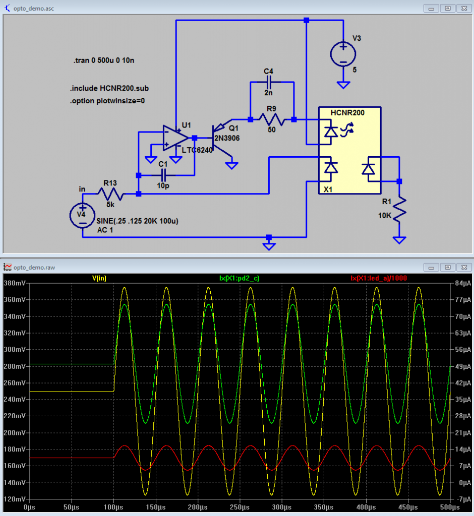
-
Circuit snippet from OP seems to be from full circuit attached:
OP snippet seems to be exactly the same.
TBH - I've not simulated it, so it may be wrong, but I wouldn't have thought an app note from vishay would have an uncorrected mistake in it for 2 years.
Just looking at the schematic I can see no issues with it.
The first stage opamps are always operated in closed feedback with a direct connection to the integrating cap
Both opamps will integrate the sum of input current + 100uA and this will cause the opamp to integrate towards the +/- rail depending on levels.
At some point the integrated ramp will cross the vbe threshold of the pnp transistors causing them to turn on which turns on the diode.
The photdiodes turn on and start stealing current from the integrator (the lower IL300 discharges its cap) and sinking that current to ground (this is where IP1 goes)
This is turn reduces the integrating current which in turn reduces the pnp drive, effectively creating -ve feedback.
The circuit stablises at the point where the pnp drive level causes the correct mount current to be integrated such that the non-inverting terminal is maintained at ground level.
Since this is just my quick look, I can be wrong.
If anyone can see a mistake or has the p-spice simulations then please share.
Edit -- Just saw the simulation (of the top half) and it seems to show the top snippet working correctly.
Could you edit to simulate the bottom half? - the bottom bit is the OP snippet.
-
compare + vs - diff input subcircuits IL300 IP1 connections to the op amps - not the same when they should be - clearly an error
and the concept is a bit strained - much better to diff on the left, just use one IL300 to isolate the single ended signal rather than having to maintain/duplicate AC and DC gain balance in circuits both sides of the isolation -
The lower leg does look imbalanced because the IL300 diverts the integrating current from a different place. In fact it stakes the lower opamp output to IP1 photodiode voltage below ground. I did notice that but didn't realise this is what you were on about. Agreed it doesn't look right.
Also agree that 1 IL300 can be used. In this case in the app note the two IL300s were used to increase the common mode rejection (cribbed from app note 55).
Did you simulate the circuit with/without the possibly incorrect connection?
edit
In fact, looking at this again, the lower opamps inner feedback loop is trying to integrate to the -ve rail (+ve input). This would turn the PNP on harder and drive more more current into the forward diode of the IL300. This would increase IP1 which would try to ground the opamp even more. If the IL300 can sink more current than the opamp can source then the opamp loses. This looks more like a mistake so well spotted.
-
Just having a look at this app note now and looks like Fig 18 on page 9 describes the use of the PNP and Fig 21 is where the circuit snippet actually comes from and may be the differential amp referred to earlier.
The PNP (if selected and biased properly) compensates for the temperature drift of the IL300 forward diode. There are explanations of using a diode in the emitter for this reason (Page 9), and a full explanation of the circuit is on page 11.
The application note says nothing of a sort:
... The output current capability of the OP-07 is extended by including a buffer transistor between the output of U1 and the LED. The buffer transistor minimizes thermal drift by reducing the OP-07 internal power dissipation if it were to drive the LED directly. ...
The forward voltage drop of the diode is irrelevant because it is inside the feedback loop. Its input referred effect will be on the order of nanovolts or less and the Vbe of the transistor will double it instead of compensating for it.
