Author Topic: Opamps - Die pictures  (Read 277823 times)

0 Members and 15 Guests are viewing this topic.

Offline NoopyTopic starter

  • Super Contributor
  • ***
  • Posts: 2402
  • Country: de
    • Richis-Lab
Re: Opamps - Die pictures
« Reply #200 on: December 10, 2021, 08:00:58 am »
Yeah, they look like brothers!  :-+

Offline NoopyTopic starter

  • Super Contributor
  • ***
  • Posts: 2402
  • Country: de
    • Richis-Lab
Re: Opamps - Die pictures
« Reply #201 on: December 18, 2021, 03:37:00 pm »
Mini-Update

I found a nice Transitron ad for their µA709 variants:


https://www.richis-lab.de/Opamp30.htm#Update

 :-/O
 
The following users thanked this post: exe, RoGeorge

Offline NoopyTopic starter

  • Super Contributor
  • ***
  • Posts: 2402
  • Country: de
    • Richis-Lab
Re: Opamps - Die pictures
« Reply #202 on: December 22, 2021, 04:19:30 am »


Q67A3S3? I didn´t find any information about this part.  :-//
The bigger T looks like Toshiba. We have seen that on the TA75558 package: https://www.richis-lab.de/Opamp28.htm


It´s a µA709 mutation! It looks quite similar to the LM709: https://www.richis-lab.de/Opamp20.htm
There is no pointer to the manufacturer.  :-//
Interesting point: They have put wide metal lines around the left, lower and right edge. Some lines are broadened and lengthened to achieve this. At the right edge there is an isolated metal line.


https://www.richis-lab.de/Opamp38.htm

 :-/O
 
The following users thanked this post: RoGeorge, capt bullshot

Offline floobydust

  • Super Contributor
  • ***
  • Posts: 9067
  • Country: ca
Re: Opamps - Die pictures
« Reply #203 on: December 22, 2021, 04:58:23 am »
EDN July 1967 has Fairchild, Motorola, Raytheon (issue cover) 709 die pics.
I didn't know the 709 op-amp was such a big deal, hitting the market Nov. 1965 and production maxxed out on 2" wafers. Bob Widlar leading the pack.
 
The following users thanked this post: Noopy

Offline NoopyTopic starter

  • Super Contributor
  • ***
  • Posts: 2402
  • Country: de
    • Richis-Lab
Re: Opamps - Die pictures
« Reply #204 on: December 28, 2021, 08:47:29 pm »


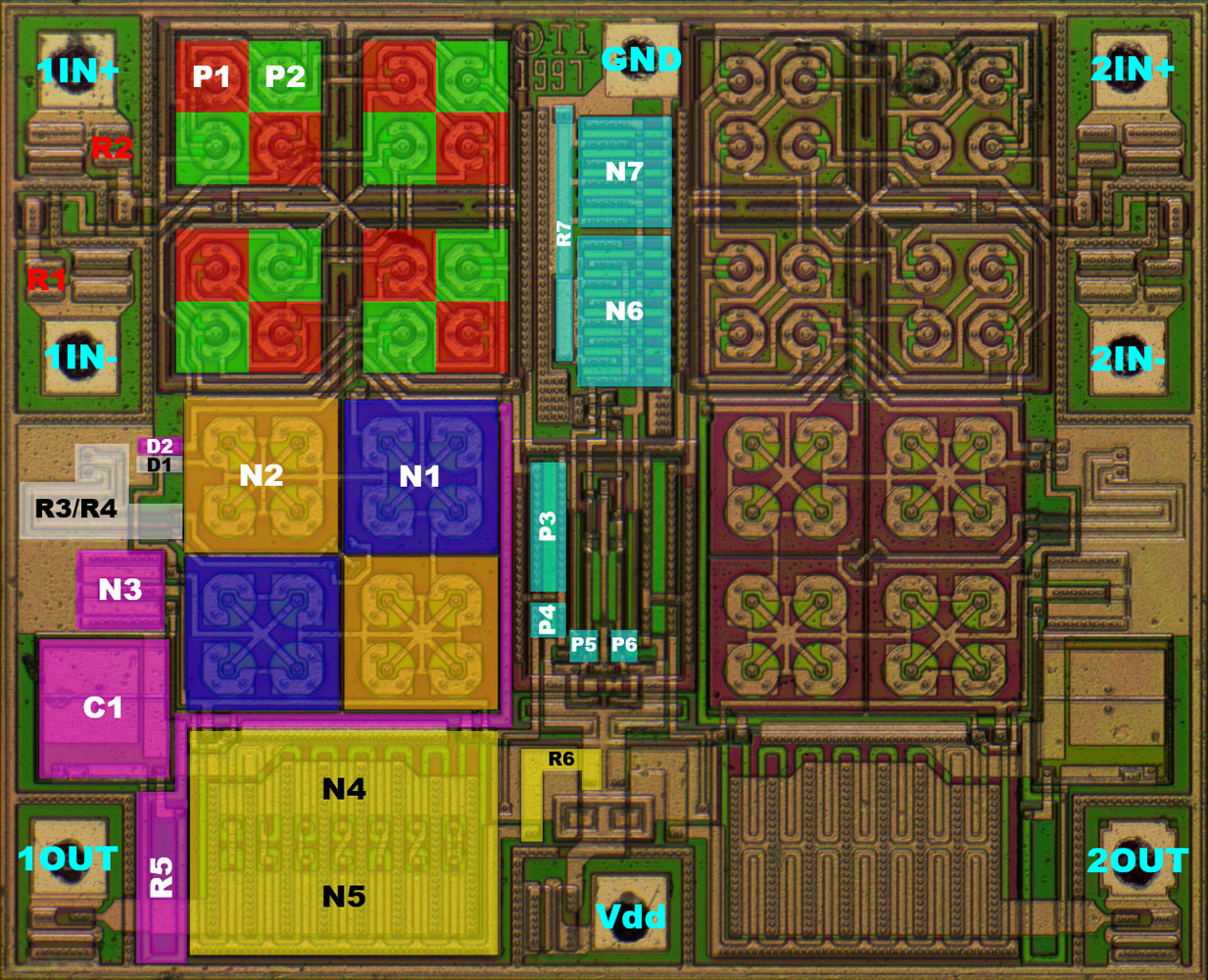
Texas Instruments TLC272, a Dual Opamp with MOSFET-Inputs.
A single supply between 3V and 16V is enough. Typical Vos is 230µV (TLC272BC, 25°C) with a TC of 1,8µV/°C. Bias current is 0,6pA typ (25°C). Bandwidth goes up to 1,3MHz - 3,4MHz depending on the variant, supply voltage and temperature.
Datasheet mentions a TLC277 with a little lower Vos: 200µV typ, 500µV max (2000µV max for the TLC272BC).


There is a schematic in the datasheet. I have added some colors.
The green circuit is the differential pair input amplifier. The zener D1 in the current mirror seems to be a current limit. In normal operation a current limitation is not necessary but at startup it´s possible that the current source P3 puts out more current than is good for the mirror for it.
The yellow circuit is the voltage amplifier. D2 is for the bias limits the output to N4. R5 and C1 are the feedback path.
In the red output stage the highside transistor is connected to the output of the VAS while the lowside transistor is connected to the input of the VAS where the signal is 180° out of phase. The output of the TLC272 can be shorted without damage. With the limiting diode D2 the lowside transistor is safe. In the supply line of the highside transistor they added the resistor R6.
The blue circuit is the bias generator. P5/P6 and N6/N7 generate the reference voltage that controls the current sources P3 and P4.


Since Texas Instruments sold the TLC272Y as bare die too there is a picture of the die in the datasheet.


The die in the TLC272 looks like the circuit in the datasheet.
Texas called the technology "Silicongate LinCMOS".


Designed 1997.


At the lower edge there is the name TLC272D. D could be a revision. In the datasheet you can see a TLC272C.


There are two small "symbols" on the die. These parts of the metal layer are not connected to anything. Perhaps really small initials?


...
« Last Edit: December 29, 2021, 09:22:04 am by Noopy »
 
The following users thanked this post: RoGeorge

Offline NoopyTopic starter

  • Super Contributor
  • ***
  • Posts: 2402
  • Country: de
    • Richis-Lab
Re: Opamps - Die pictures
« Reply #205 on: December 28, 2021, 08:48:32 pm »


You can find every part of the schematic on the die. Especially interesting are the input transistors P1/P2 and the current mirror transistors N1/N2. There are four times four input transistors criss-cross connected for low TC of Vos. N1/N2 are less meshed but still criss-cross connected.
In the middle of the die there is the biasing circuit which is used by both opamps, the right one and the left one.
At the lower edge there is the output stage.
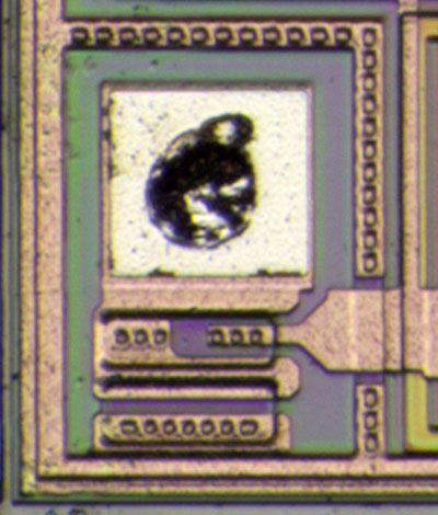


The output bondpad and the Vdd bondpad are equipped with a ESD protection MOSFET. While the "normal" MOSFETs have silicon gates this one has a metal gate. The thicker gate oxide increases the threshold voltage so that the MOSFET conducts at higher voltages. The line into the opamp circuit isn´t connected directly to the bondpad but to the doped area of the MOSFETs. That gives you a little higher impedance for an ESD pulse.
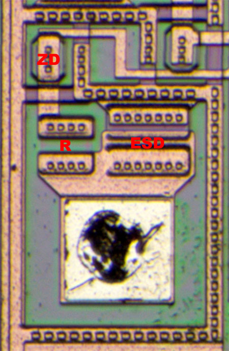


At the input bondpads there is an additional protection with a series resistor and a small component, probably a zener diode.
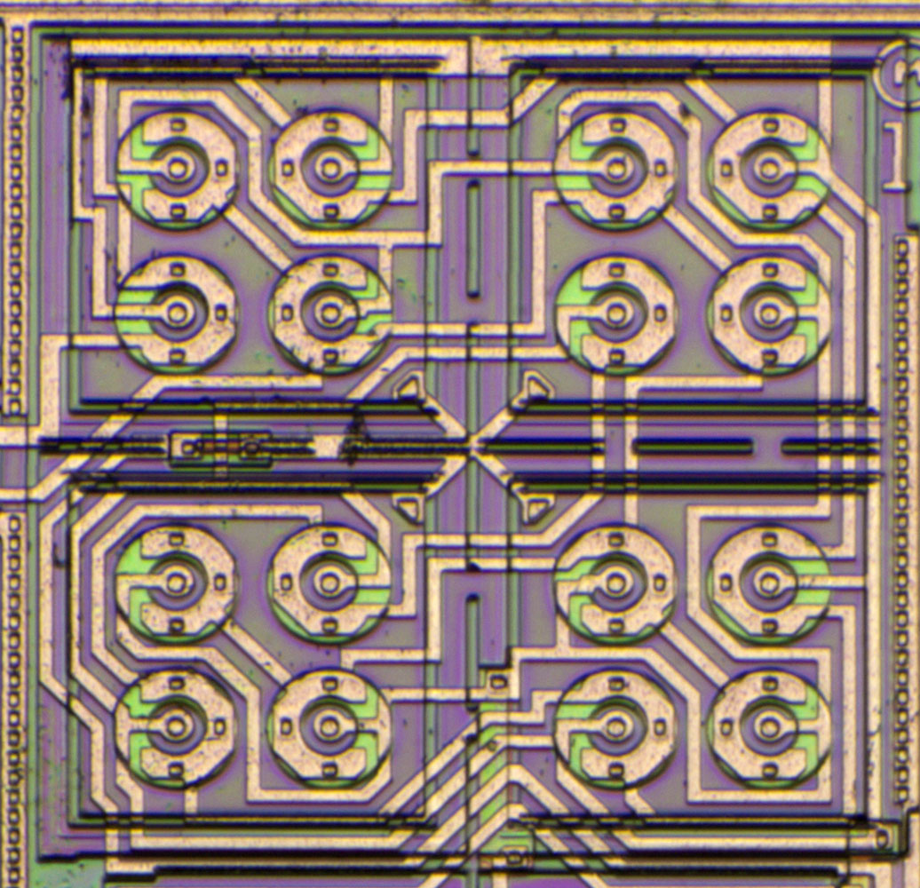


The input MOSFETs have circular gate electrodes.
The criss-cross connection made the interconnection quite complex.
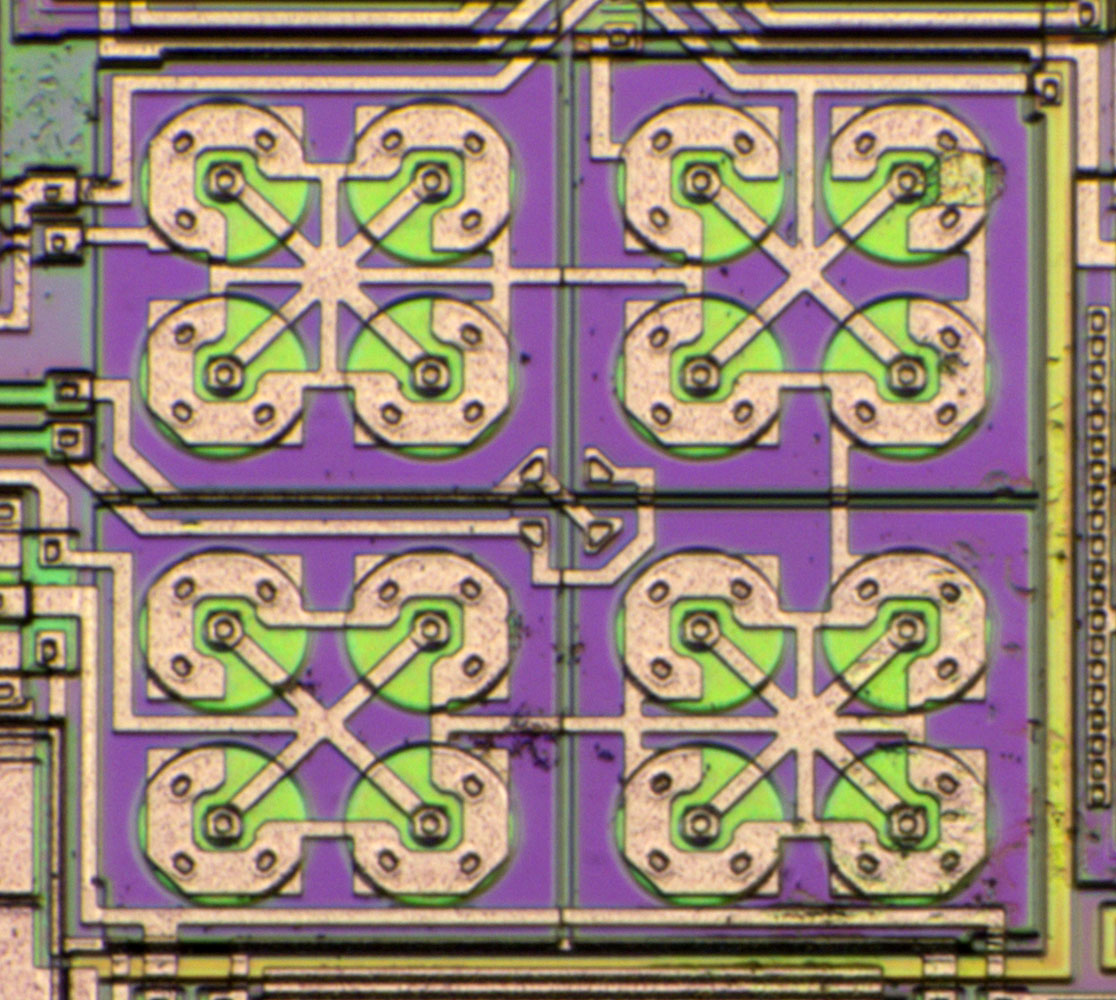


The n-MOS of the current mirror have bigger gate electrodes than the p-MOS at the input. Interesting...
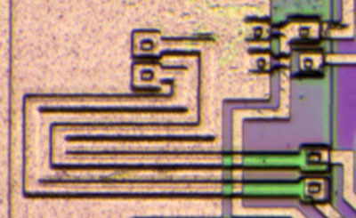


The source resistors of the current mirror are placed left of the transistors. The datasheet describes a "Trimmed Offset Voltage". If you want to tune Vos you have to tune these source resistors but it´s impossible to tune resistors this small.  :-// And I didn´t find an other tunable circuit on the die.  :-//
In the line under "Trimmed Offset Voltage" the datasheet describes the Vos of the TLC277. Perhaps the TLC277 die is different and tuneable.
In the upper right corner there are the two zener diodes.
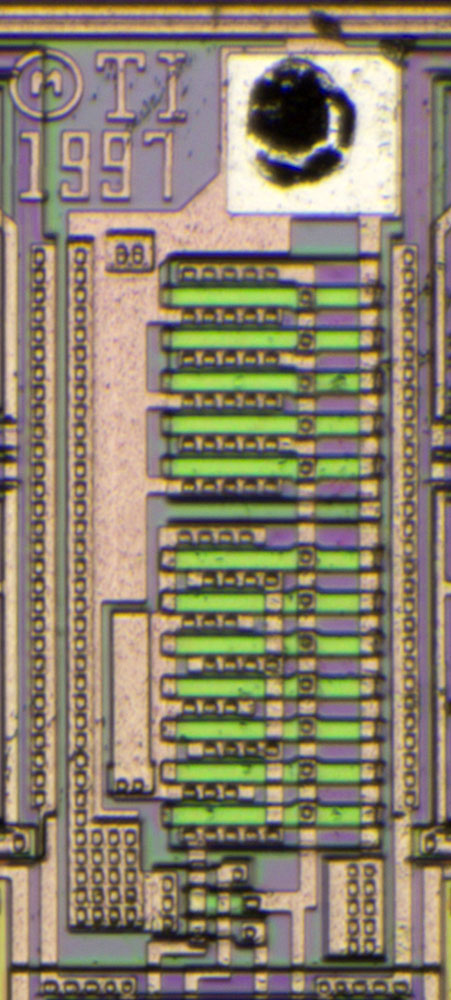


Lowside current mirror of the reference circuit.
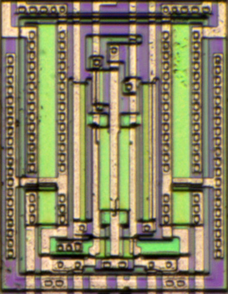


At the lower edge of the picture there is the highside current mirror.
The two big transistors on the left side are the two current sources for the left opamp (...on the right side for the right opamp).
Between the current sources there are some smaller transistors not shown in the schematic. That´s probably a startup circuit.
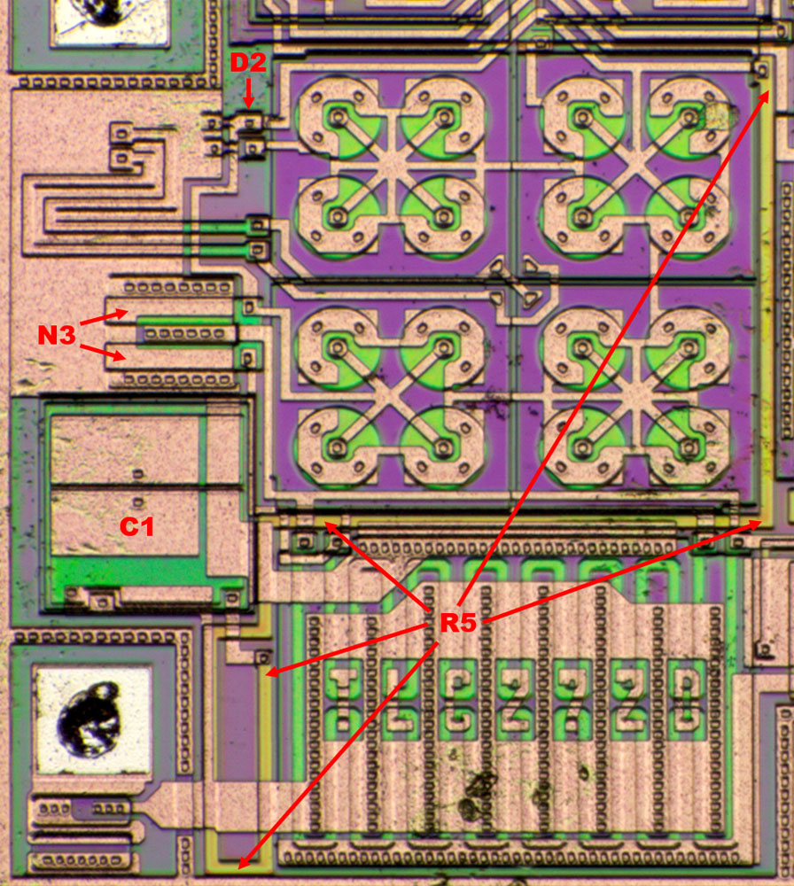


The feedback resistor R5 is interesting: It travels a long way through the circuit.
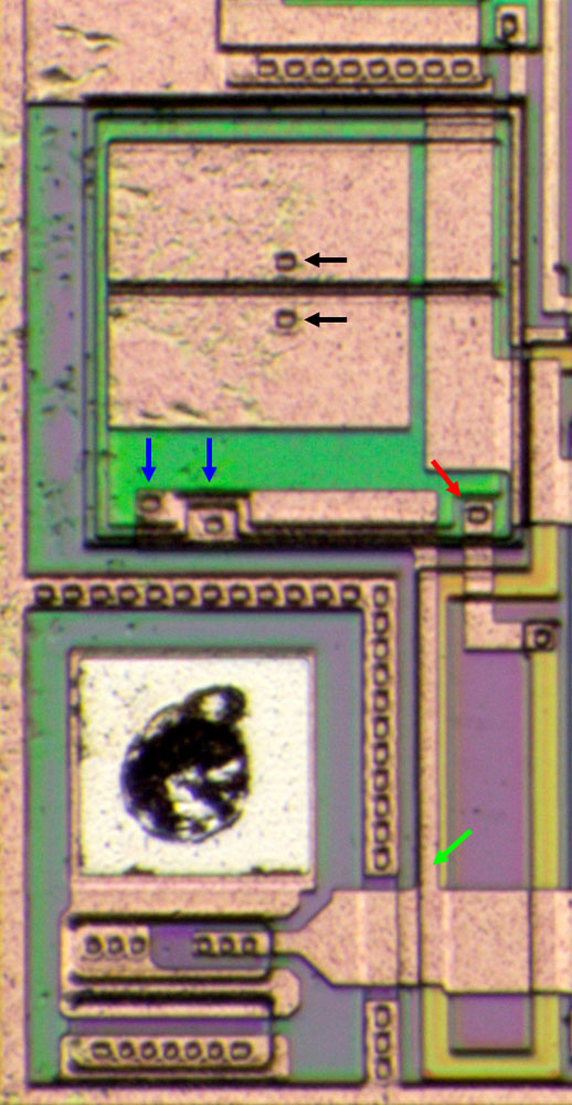


The feedback capacitor C1 is built with three electrodes. The output (green) is connected to the upper and the lower electrode (blue). The resistor R5 is connected to the electrode in the middle (red). The upper electrode is split and connected with a metal rectangular (black). That´s probably a way to tune the capacitance.
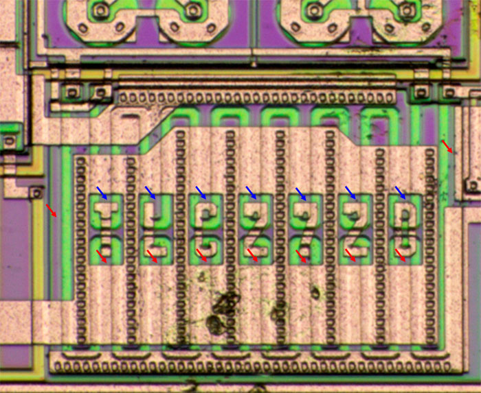


The highside transistor (red) and the lowside transistor (blue) are integrated in the same area. The highside transistor is a little bigger.
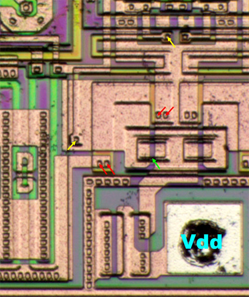


The resistor R6 is a wide stripe between the output transistor and Vdd (red). There is a metal plate on top of this resistor. The plate is connected to Vdd with a resistor (yellow). On the right side there is a strange part (green) between the plate and Vdd.  :-//
My best guess is that this metal is kind of a gate electrode that bias the resistor.  :-//


https://www.richis-lab.de/Opamp39.htm

 :-/O
 
The following users thanked this post: RoGeorge, magic

Offline David Hess

  • Super Contributor
  • ***
  • Posts: 19216
  • Country: us
  • DavidH
Re: Opamps - Die pictures
« Reply #206 on: December 28, 2021, 10:05:26 pm »
The n-MOS of the current mirror have bigger gate electrodes than the p-MOS at the input. Interesting...

To equalize gate capacitance for similar dynamic performance?

Quote
The highside transistor (red) and the lowside transistor (blue) are integrated in the same area. The highside transistor is a little bigger.

The p-channel transistors need to be larger for the same channel resistance and transconductance.  Even so, the datasheet reports a high side dropout that is a lot greater than the low side dropout.
 

Offline magic

  • Super Contributor
  • ***
  • Posts: 8063
  • Country: pl
Re: Opamps - Die pictures
« Reply #207 on: December 28, 2021, 10:51:55 pm »
Nice. I have a bunch of TS27L2, which is ST's version of the low power variant ("L"). The single (TLC/TS271) has a pin for adjusting internal bias and performance, offset nulling is available as well. I use them instead of LM358 when power consumption matters and I want to use THT because too lazy to make a custom PCB. They also have better "typical" precision specs than the cheapest of bipolar parts, thanks no doubt to the complex cross-coupling of 1st stage transistors.

D2 may be involved in output sink current limiting (by clamping Vgs of N4), what's the point of D1 I don't know. Not sure if I buy the theory that P3 can source more current than is safe for the mirror.

The n-MOS of the current mirror have bigger gate electrodes than the p-MOS at the input. Interesting...
This means more effective channel length. And also less channel width, because the central circle has less circumference. Both have some influence on characteristics of the FET, I think higher drain output impedance or something like that.

There is this article with some information about CMOS opamp design, including what AFAIK is the classic R2R output stage still used to this day in most chips.
http://class.ece.iastate.edu/djchen/EE501/2011/MonticelliRailToRailOutSwing.pdf


The p-channel transistors need to be larger for the same channel resistance and transconductance.  Even so, the datasheet reports a high side dropout that is a lot greater than the low side dropout.
This is not an R2R output, both transistors are N-channel, top is source follower.

It's a single supply opamp. And it struggles with sinking current when input common mode is near ground, which I believe is because source potential of P1/P2 limits the maximum gate voltage that can be applied to N4.
 

Offline NoopyTopic starter

  • Super Contributor
  • ***
  • Posts: 2402
  • Country: de
    • Richis-Lab
Re: Opamps - Die pictures
« Reply #208 on: December 29, 2021, 06:55:35 am »
...TS27L2, which is ST's version...

I will have to take a look into this one too.  :D


D2 may be involved in output sink current limiting (by clamping Vgs of N4), what's the point of D1 I don't know. Not sure if I buy the theory that P3 can source more current than is safe for the mirror.

You are right, the big current mirror probably won't get hurt but the current source P3 could kill itself.
D2 for output current limit? Hm, I'm not sure about that... For me that looks more like a bias voltage generator for the VAS.


It's a single supply opamp. And it struggles with sinking current when input common mode is near ground, which I believe is because source potential of P1/P2 limits the maximum gate voltage that can be applied to N4.

 :-+

Offline magic

  • Super Contributor
  • ***
  • Posts: 8063
  • Country: pl
Re: Opamps - Die pictures
« Reply #209 on: December 29, 2021, 08:47:36 am »
Monticelli states on page 4 that similar diode (Z1) is used to limit output current in LMC660. There is a similar Z2 at the high side P-MOS too, but not mentioned in the text.

VAS bias is set by the current source P4, as usual. The input stage will drive N3 to exactly sink all P4 current so that N5 source follower gate voltage stays where it needs to be. Output bias is determined by N4 being driven in parallel with N3. N4 is maybe 10x larger so it sinks 10x the VAS current. When the output is unloaded (or sourcing) that current will come from N5.
 
The following users thanked this post: Noopy

Offline NoopyTopic starter

  • Super Contributor
  • ***
  • Posts: 2402
  • Country: de
    • Richis-Lab
Re: Opamps - Die pictures
« Reply #210 on: December 29, 2021, 09:19:16 am »
I agree with your explanation and Mr. Monticelli paper.
Thanks for the correction.
 :-+


Offline NoopyTopic starter

  • Super Contributor
  • ***
  • Posts: 2402
  • Country: de
    • Richis-Lab
Re: Opamps - Die pictures
« Reply #211 on: January 01, 2022, 06:23:50 pm »


We have talked about the TLC272. If you need more opamps you can take the TLC274 with four of them.
If you need a lower Vos you take the TLC279. Interesting point: The TLC279 has a higher Vos than the TLC277.


In the datasheet you find a picture of the metal layer. Nice!  8)


The die looks quite similar to the picture of the metal layer.


TI doubled the TLC272. There are just a few differences.


TLC274B, the picture in the datasheet shows a revision H!  :o


I was right! These "things" we have already seen in the TLC272 are symbols! That´s a H and a fat I?


Beside the GND bondpad there is a testpad with a single transistor. Source and Gate are connected to GND.


The bulk of the input transistors (right) are connected with Vdd more massively than in the TLC272
Generally the transistors are connected more massively.


Here we have the two source resistors (green), the capacitor (red) and the VAS transistor (cyan) we know from the TLC272. Everything is a little different but not in principle.


The bias circuit can be found in the middle of the die.


Here we have the highside current mirror of the reference circuit on the right side and the much smaller lowside current mirror on the left side. Between the current mirrors there is the circuit that probably guarantees a proper startup.


Left and right of the reference circuit there are the current source transistors.


And here we have the obscure circuit that we have seen in the TLC272 too.
There is a strange element (blue) connected to Vdd directly and connected to Vdd through a resistor (red).
With this picture we can be sure that the circuit doesn´t influence the resistor R6 since the resistor is too far away (cyan).
Here we have two testpads to contact the strange element.


On the right side of the die there is the same circuit.
But what the hell is the point of this circuit???   :-//


https://www.richis-lab.de/Opamp40.htm

 :-/O
 
The following users thanked this post: SeanB, RoGeorge

Offline magic

  • Super Contributor
  • ***
  • Posts: 8063
  • Country: pl
Re: Opamps - Die pictures
« Reply #212 on: January 01, 2022, 07:35:12 pm »
eBay strikes again :-DD

Any chance that the mystery circuit is some sort of ESD protection? Like clamping overvoltage on VDD? I recall seeing such things in datasheets.
BTW, I found official schematic of LinCMOS per-pin protection in TLC3072 datasheet, but nothing about overvoltage protection.
 

Offline NoopyTopic starter

  • Super Contributor
  • ***
  • Posts: 2402
  • Country: de
    • Richis-Lab
Re: Opamps - Die pictures
« Reply #213 on: January 02, 2022, 10:24:30 am »
I thought about some overvoltage protection too but that would be placed near the Vdd pad and there is already a ESD protection.
Perhaps that is a circuit that is needed at the output stages. That would explain why these two "things" are placed at the left and right edge. A strange parasitic behaviour of the output stage? Removing free charges?  :-//

Offline NoopyTopic starter

  • Super Contributor
  • ***
  • Posts: 2402
  • Country: de
    • Richis-Lab
Re: Opamps - Die pictures
« Reply #214 on: January 05, 2022, 04:25:29 am »


SN72709, another µA709 variant built by Texas Instruments.
The N stands for the epoxy package.


Yeah, that´s a 709. There is nothing special.


The specs of the AN variant are a little better.


The die is the same. Texas Instruments did just some binning.


https://www.richis-lab.de/Opamp41.htm

 :-/O
 
The following users thanked this post: SeanB, RoGeorge

Offline David Hess

  • Super Contributor
  • ***
  • Posts: 19216
  • Country: us
  • DavidH
Re: Opamps - Die pictures
« Reply #215 on: January 05, 2022, 05:24:28 am »
I am always surprised that the 709 was as popular as it was considering its quirks and difficulty in using it safely.  Walter Jung discussed its history a little bit.
 

Offline NoopyTopic starter

  • Super Contributor
  • ***
  • Posts: 2402
  • Country: de
    • Richis-Lab
Re: Opamps - Die pictures
« Reply #216 on: January 05, 2022, 09:59:48 am »
Well it looks like back in the days it was good enough. Seems it was one of the beststeller.

Offline MegaVolt

  • Frequent Contributor
  • **
  • Posts: 933
  • Country: by
Re: Opamps - Die pictures
« Reply #217 on: January 24, 2022, 11:41:14 am »
Do you plan to photograph ADA4530? Or was it possible to celebrate photos on the Internet?
 

Offline NoopyTopic starter

  • Super Contributor
  • ***
  • Posts: 2402
  • Country: de
    • Richis-Lab
Re: Opamps - Die pictures
« Reply #218 on: January 24, 2022, 11:53:56 am »
Looks like an interesting part.  :-+ I can put it on my list. Right now it seems like you can´t by it anywhere...
 
The following users thanked this post: MegaVolt

Offline NoopyTopic starter

  • Super Contributor
  • ***
  • Posts: 2402
  • Country: de
    • Richis-Lab
Re: Opamps - Die pictures
« Reply #219 on: February 13, 2022, 08:07:25 pm »


SGS ATEX L141, another µA741 mutation.


Datasheet shows the same schematic as printed in the datasheet of the National Semiconductor LM741 (https://www.richis-lab.de/Opamp23.htm).
(It´s not the circuit integrated in the LM741.  :))


The bondwire of the positive supply has seen a little too much current.


The die is quite similar to the Sescosem SC2741 (https://www.richis-lab.de/Opamp07.htm). Perhaps they worked together. Sescosem became Thomson Semiconductor and merged with SGS.

I don´t see major damage. The color of the bondpad in the lower right corner is a little strange but that´s probably just a process weakness.


R4 defines the current in the differential input stage and in the L141 it can be adjusted.


https://www.richis-lab.de/Opamp42.htm

 :-/O
 
The following users thanked this post: SeanB, RoGeorge

Offline T3sl4co1l

  • Super Contributor
  • ***
  • Posts: 22435
  • Country: us
  • Expert, Analog Electronics, PCB Layout, EMC
    • Seven Transistor Labs
Re: Opamps - Die pictures
« Reply #220 on: February 13, 2022, 09:47:18 pm »
Is that maybe some melty metallization on the top edge, towards the left?  Not sure what that is, if it's just some odd structure or actually kinda balled up.  Yeah, no or not obvious damage, after all the bondwire broke first so the die can't be toooo cooked.  I wonder if that would require reverse biasing (i.e. a mere diode drop into whatever other pins), maybe someone wired it wrong. ;D

Tim
Seven Transistor Labs, LLC
Electronic design, from concept to prototype.
Bringing a project to life?  Send me a message!
 

Offline NoopyTopic starter

  • Super Contributor
  • ***
  • Posts: 2402
  • Country: de
    • Richis-Lab
Re: Opamps - Die pictures
« Reply #221 on: February 14, 2022, 05:04:30 am »
Is that maybe some melty metallization on the top edge, towards the left?

I don´t think so, but I´m not sure too.  :-//


I wonder if that would require reverse biasing (i.e. a mere diode drop into whatever other pins), maybe someone wired it wrong. ;D

That sounds very plausible to me.  :-+


Online mawyatt

  • Super Contributor
  • ***
  • Posts: 6115
  • Country: us
Re: Opamps - Die pictures
« Reply #222 on: February 14, 2022, 02:39:01 pm »
I wonder if that would require reverse biasing (i.e. a mere diode drop into whatever other pins), maybe someone wired it wrong. ;D

Tim

Think this is what happened since the apparent VCC wire bond melted. VEE should be the die substrate which can handle significant current.

Best,
Curiosity killed the cat, also depleted my wallet!
~Wyatt Labs by Mike~
 

Offline NoopyTopic starter

  • Super Contributor
  • ***
  • Posts: 2402
  • Country: de
    • Richis-Lab
Re: Opamps - Die pictures
« Reply #223 on: February 23, 2022, 08:26:01 pm »


One more comparator, the Fairchild µA311. Single supply 5V-36V is possible. Like the LM306 (https://www.richis-lab.de/Opamp09.htm) the µA311 can drive a load directly. It can isolate 50V conduct 50mA and is protected against short circuits for 10s.


The datasheet contains a schematic. I have colored it. The input stage contains additional resistors to do offset compensation. Datasheet explains you alternatively can use this inputs to rise the bias current and with it the slew rate.

There are two more stages (pink/grey) working with an bias current generated with Q23 and Q21 (blue). The current sinks are based on a reference voltage generator (yellow).

The output of the grey stage can be drained with Q7 (red). That´s the strobe feature. The cyan stage locks itself.

The output stage (dark red) contains the driver transistor Q12 and the output transistor Q15. The green circuit is the current limit. The purple circuit makes sure the driver transistor isn´t driven too hard so is still can be switched off fast.


The die is 1,6mm x 1,2mm. At the lower edge there are some test structures. In the upper right corner there is a test transistor.

On the right side there is the huge output transistor. You can see an additional frame probably similar to the LM306 output transistor, probably a base doping, a light p doping rising the breakdown voltage.


https://www.richis-lab.de/Opamp43.htm

 :-/O
 
The following users thanked this post: SeanB, TurboTom, RoGeorge, capt bullshot

Offline NoopyTopic starter

  • Super Contributor
  • ***
  • Posts: 2402
  • Country: de
    • Richis-Lab
Re: Opamps - Die pictures
« Reply #224 on: February 27, 2022, 06:52:07 pm »


The PMI OP400 contains four opamps and is now built by Analog Devices. The offset voltage is 150µV typ. The current consumption is 725µA max. Open Loop Gain is 5000V/mV. Bias current is just 3nA (bipolar input) and you are allowed to load the output with 10nF.


The schematic you can find in the datasheet.


The die is 4,5mm x 3,1mm. You can clearly see the four opamps.


In the center of the die there is the reference for the bias current sources.


In the middle of each opamp you can see the four criss-cross connected input transistors (red). They look a little like PNP but they are NPN.
You can also find a small transistor with two emitter (green) which source some bias current.
The voltage limiting network is marked with a white arrow.

In the lower area there are two testpads which were probed. It looks like you can check the offset in the voltage amplifier stage.

In the upper left corner there are the big structures of the output stage.


https://www.richis-lab.de/Opamp44.htm

 :-/O
 
The following users thanked this post: SeanB, RoGeorge, magic


Share me

Digg  Facebook  SlashDot  Delicious  Technorati  Twitter  Google  Yahoo
Smf


-->