Finally I managed to update the AMP01. It was one of my first projects and first I had just "normal" pictures just showing the metal layer. I wrote A LOT of words around the pictures but that didn´t compensate the lack of information. Since the AMP01 is a really nice part it deserves better pictures and explanations:
The AMP01 is an instrumentation amplifier developed by Precision Monolithics, which still costs over 30€ today and is now distributed by Analog Devices.
The datasheet specifies a maximum offset voltage of 50µV. The temperature drift is a maximum of 0,3µV/°C. The bias current remains below 4nA. The amplification factor can be selected between 0,1 and 10.000. With a gain factor of 1.000, the linearity is sufficient for an accuracy of 16Bit. The datasheet specifies a common mode rejection of at least 125dB. An output level of up to +/-10V is regulated with up to +/-50mA. A maximum of +/-13V is possible. Capacitive loads of up to 1µF are also permissible. For a gain factor of 1.000, the datasheet specifies a -3dB bandwidth of typically 26kHz. The slew rate is 4,5V/µs (G=10). The settling time is 50µs (G=1000, 20V, +/-0,01%).
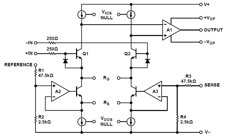
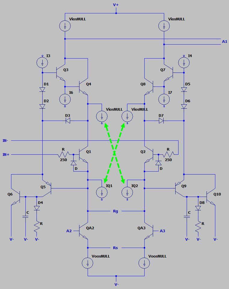
The datasheet of the AMP01 contains a block diagram that shows how the amplifier works. In the centre there are two balanced amplifier branches that process the input signals. The amplification factor of this differential amplifier and thus of the entire component can be adjusted via the resistance between the branches. This is called "cross degeneration" or "pi degeneration".
The two branches are supplied by two current sources. Two current sinks are located at the lower ends of the differential amplifier branches. Both pairs of current sources can be adjusted independently of each other, thus enabling the offset voltages at the input and output of the AMP01 to be balanced. According to the datasheet, the current ratio above the input transistors can be used to compensate for the offset voltage at the input, which is then multiplied by the amplification factor. It is noticeable that the circuit diagram just represents reality in a very simplified way. Here, the upper current sources would just influence the offset voltage at the output. The set amplification factor would have no influence.
With the current ratio below the input transistors, one can compensate the offset voltage at the output. A different current ratio leads to a current flow across the resistor Rs, which in its main function defines the strength of the sense feedback. This also makes it possible to adjust the offset voltage at the output.
For gain factors above 50, the datasheet recommends adjusting the offset voltage at the input. For amplification factors below 50, however, the offset voltage at the output should be adjusted, as this is initially higher if the amplification factor is left out. If you want to adjust both offset sources, start with a short-circuited resistor Rg at the input offset, then remove the short-circuit and adjust the output offset.
Below the input transistors there are two additional transistors that influence the signals in the branches. On the right side is the sense potential, which is connected directly to the output or, in the case of four-wire connection, to the actual destination point of the output signal. Since the AMP01 can drive relatively high currents, such feedback of the output signal is quite useful. The transistor in the left path is controlled by the reference pin. This potential can be connected directly to the local ground or, with four-wire connection, to the reference potential at the destination point.
The levels of the sense and reference potentials are adjusted via voltage dividers that are integrated on the chip. This means that no particularly constant resistors are required externally. There is usually hardly any voltage at the reference input, but an identical voltage divider has been integrated on this side as well. This design ensures the best possible symmetry. Temperature drifts have the same effect on both sides and compensate each other. This is another advantage of integration on the chip. Both voltage dividers thus have very similar temperatures. The operational amplifiers between the voltage dividers and the differential amplifier branches ensure that the high-impedance voltage dividers are not loaded.
A resistor is to be connected to the contacts Rs, which acts as an emitter resistor like Rg, but is assigned to the transistors above it in the feedback paths. Like Rg, Rs represents a local negative feedback. However, since the local negative feedback at Rs relates to the global negative feedback, Rg and Rs have an inverse effect. A low resistance Rg results in a high amplification factor. A low resistance Rs provides a low amplification factor. The opposite influence on the amplification has the positive side effect that thermal drifts of the resistors at least partially compensate each other.
There is a buffer amplifier at the output of the differential amplifier. On the one hand, this prevents the load at the output of the differential amplifier from having a negative effect on its specifications. On the other hand, the buffer amplifier also makes it possible to connect higher loads to the instrumentation amplifier. This can be a 50Ohm system, but it can also just be a longer transmission line with a large parasitic capacitance.
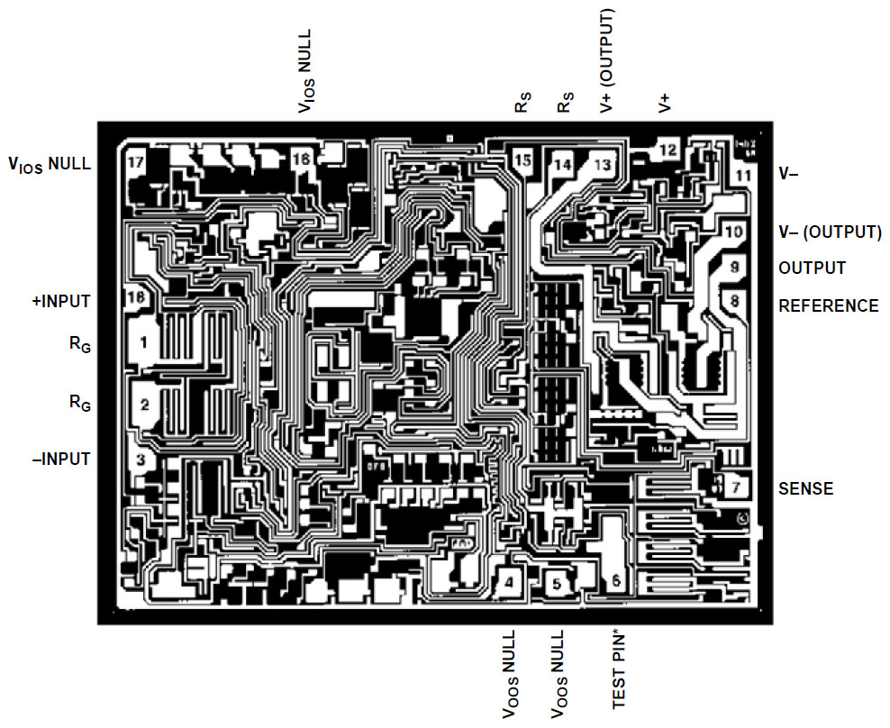
The datasheet shows the metallisation layer of the instrumentation amplifier. The dimensions of the die are therefore 2,82mm × 3,78mm.
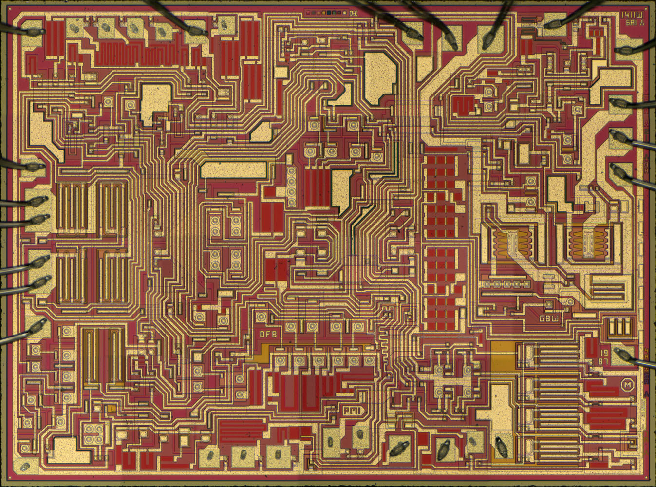
The present die corresponds pretty much exactly to the representation in the datasheet.
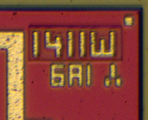
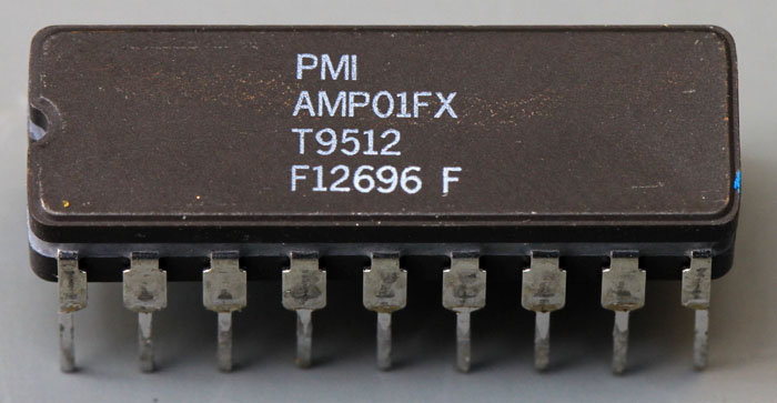
1411 is the internal designation of the circuit. The W indicates the revision. In the case of PMI, this was done by counting up from Z in the direction of A. This is therefore the fourth revision.
The character string 6A1 stands for the mask of the metal layer. On the right edge of the dies are the abbreviations of eight other masks.
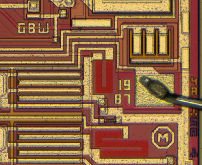
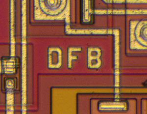
The design dates back to 1987. GBW and DFB are probably abbreviations of the developers involved. Two patents mentioned in the datasheet belong to Derek F. Bowers.
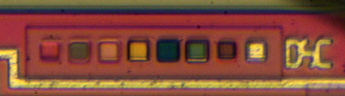
On the upper edge, the masks depict eight small squares. Next to them is an integrated symbol that cannot be assigned.
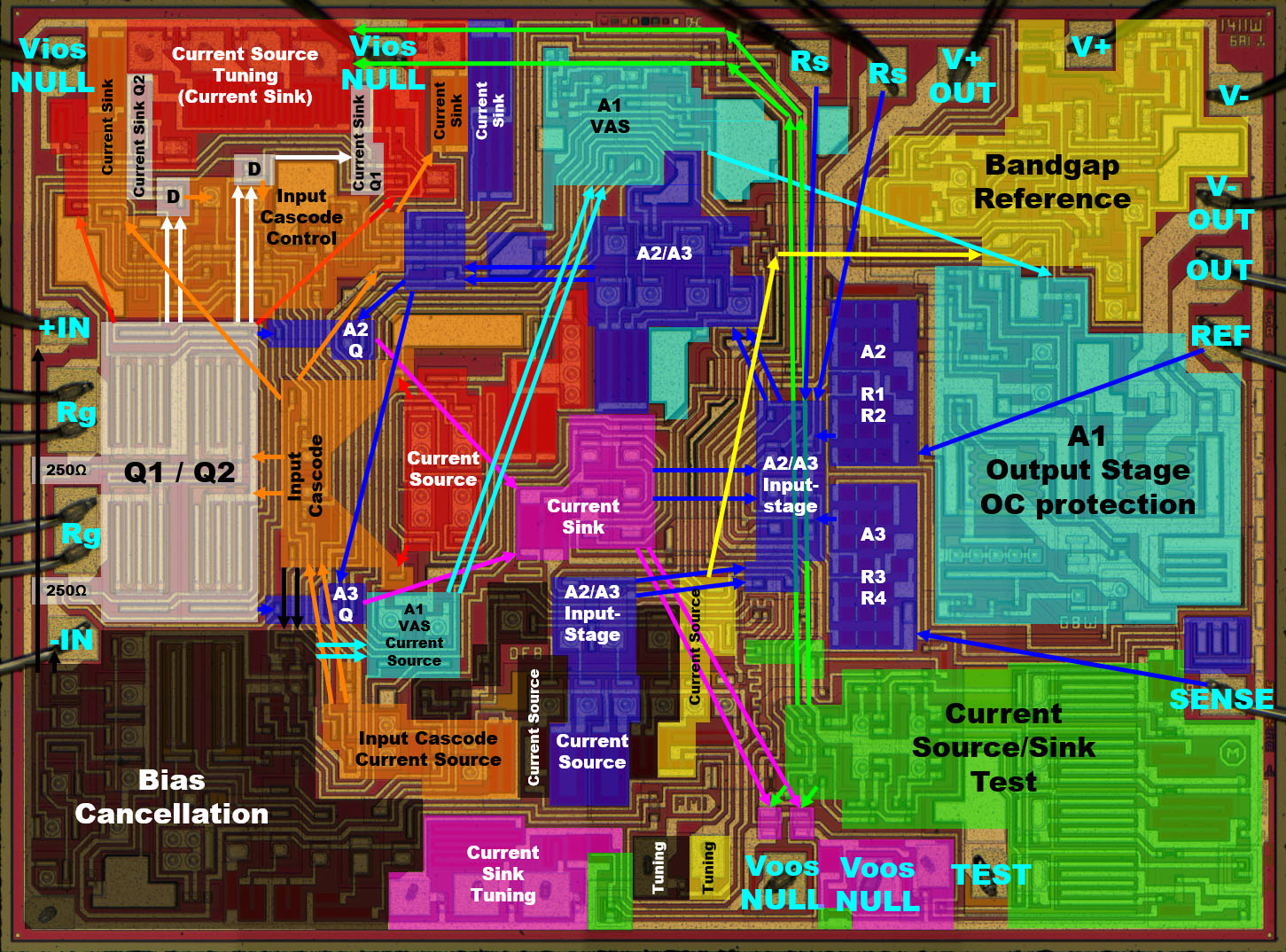
At first glance, the layout of the die appears confusing, but the critical circuit parts are arranged very advantageously. The majority of the critical elements are integrated symmetrically around the horizontal axis in the center of the device. If the output stage on the far right heats up, the differential paths experience a similar temperature change and drift defects compensate to a large extent.
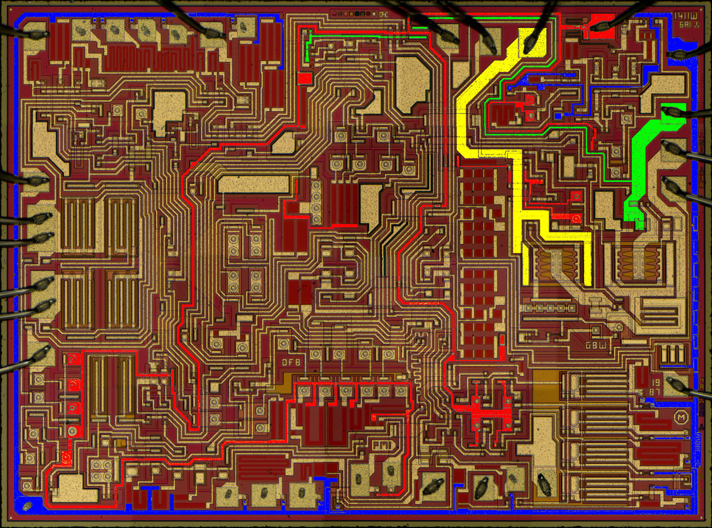
The AMP01 offers two supply interfaces. One interface supplies only the output stage (yellow/green). The other interface supplies the remaining circuit parts (red/blue).
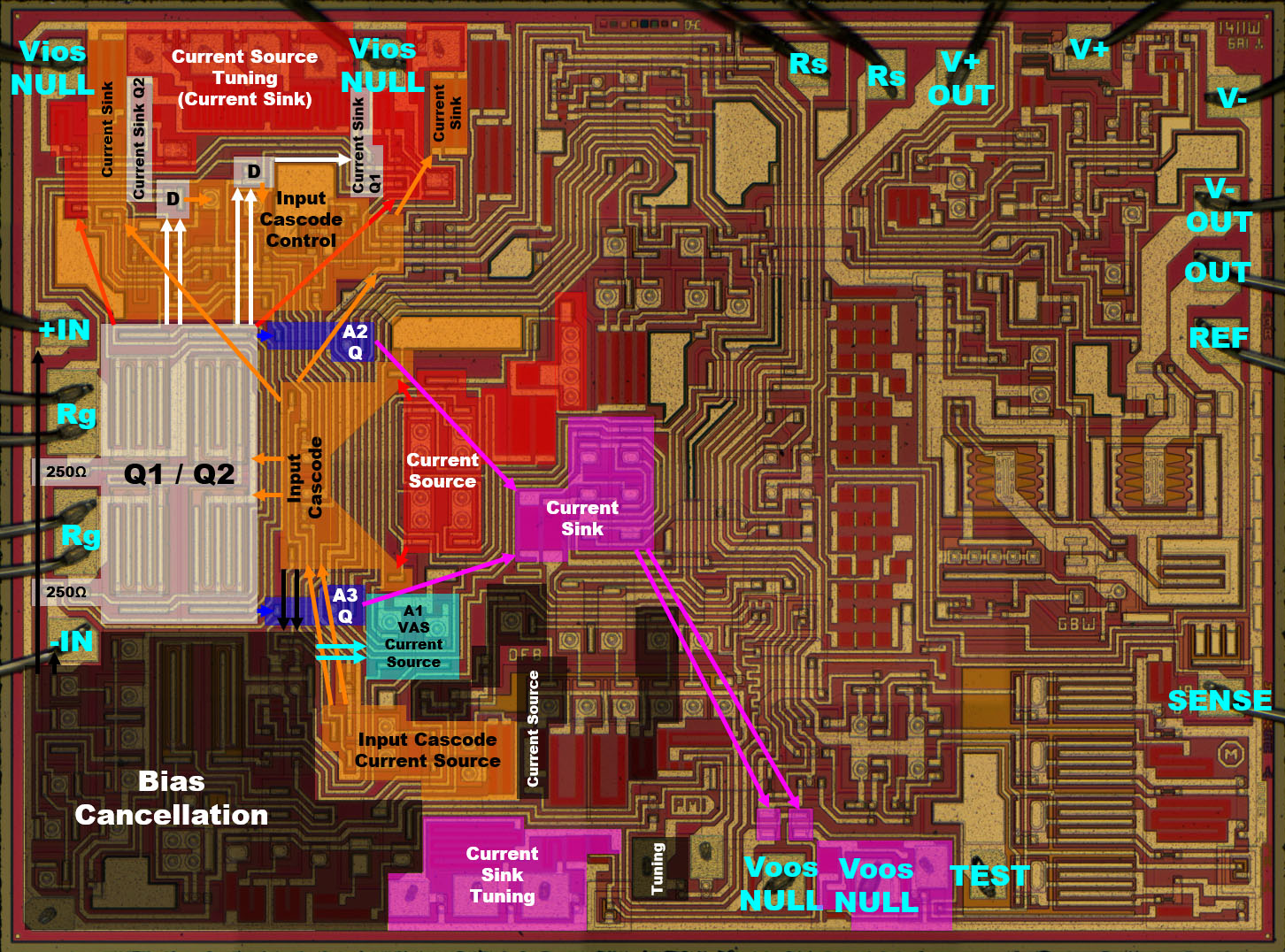
The input transistors are positioned with their input resistors on the far left (white). The protection diodes are positioned a little to the top. The feedback control transistors (blue) connect the input transistors to the current sinks (pink). The current sinks themselves are in the middle of the die. At the lower edge, an adjustment takes place during production. In addition, the potentials that enable an external adjustment intervene here.
The current sources that supply the input transistors are located between the input transistors and the current sinks (red). Again, there are circuit parts for an adjustment during production and the intervention for an adjustment in the later application. Both are located in the upper left corner of the die. However, it is not the current source that is influenced there, but more or less current sinks connected in parallel.
The input transistors are protected from voltage fluctuations at the collector by a cascode circuit (orange). This part of the circuit is not shown in the datasheet. It is located between the input transistors (white) and the current sources (red).
The coupling of the signals to the output amplifier (cyan) is done from the circuit part that do the input current compensation. The input current compensation is located in the lower left corner and takes up quite a large area (black). The circuit feeds the necessary base currents into the inputs of the instrumentation amplifier. The compensation circuit works with two current sources placed further to the right, one of which can be adjusted via a test pad. According to the circuitry, the strength of the compensation can be adjusted here.
If we record the circuit of the large differential amplifier, we get the circuit diagram shown here. There are many more current sources and sinks in the circuit than shown in the datasheet. They do biasing in many places.
As expected, the offset voltage at the input is not adjusted directly at the current sources ViosNULL. The two current sinks ViosNULL are located above the input transistors and the two current sinks IQ1/IQ2 are integrated below. To adjust the offset, the current ratio of these pairs is changed. Changes have an inverse effect on ViosNULL and IQ1/IQ2. Ultimately, the input offset is influenced via the current sinks IQ1/IQ2, whose differential current flows through the resistor Rg. The current sinks ViosNULL ensure that the current ratio in the upper area isnot excessively influenced.
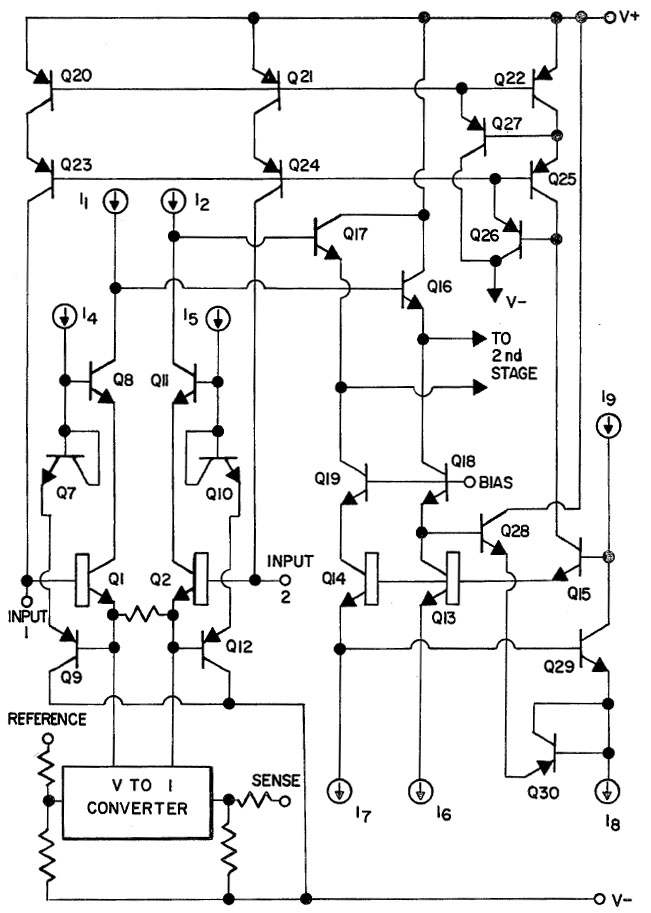
The design and characteristics of the input amplifier are described in more detail in patent US4471321. This patent is mentioned in the datasheet of the AMP01. The circuit fulfils two important tasks in addition to the basic function of a differential amplifier. It ensures that the potentials at the input transistors change as little as possible and that the external circuitry is loaded as little as possible by the input currents.
The cascode circuit in the immediate vicinity of the input transistors fixes their collector-emitter voltage and thus ensures strong common-mode rejection (I4/Q8/Q7/Q9 and I5/Q11/Q10/Q12).
In the right-hand section, the input circuit is shown a second time. In the centre are two SuperBeta transistors (Q14/Q15), as they are also used at the inputs of the AMP01 (Q1/Q2). In this connection, they draw a base current that corresponds to the base current of the input transistors. It does not have to be the absolute same current value, but the ratio of the currents has to be the same. Necessary amplification factors can be set by the following current mirrors. The bias cancellation thus ensures that a current is fed into the inputs of the AMP01 that corresponds fairly exactly to the base current of the input transistors. This ensures that the circuit at the inputs of the AMP01 is not loaded with the base currents.
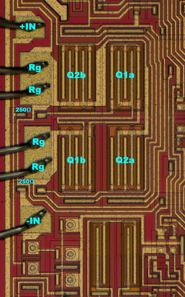
The two input transistors Q1 and Q2 are each divided into two areas arranged crosswise so that temperature gradients affect both branches of the differential amplifier as equally as possible.
The external resistor Rg, which also determines the amplification factor, is connected with two bondwires. Since Rg may have quite a small value, special care must be taken to ensure that the influence of the connection lines and thus also of the bondwires remain as small as possible.
[...]


