Author Topic: Opamps - Die pictures  (Read 279554 times)

0 Members and 8 Guests are viewing this topic.

Offline NoopyTopic starter

  • Super Contributor
  • ***
  • Posts: 2404
  • Country: de
    • Richis-Lab
Re: Opamps - Die pictures
« Reply #750 on: August 08, 2025, 06:58:58 pm »
Rectangular shapes can't amplify a smooth sound! The edges are too sharp.  ;D

Offline David Hess

  • Super Contributor
  • ***
  • Posts: 19218
  • Country: us
  • DavidH
Re: Opamps - Die pictures
« Reply #751 on: August 08, 2025, 07:13:29 pm »
That explains why my diamond buffers sound sharp.
 

Offline NoopyTopic starter

  • Super Contributor
  • ***
  • Posts: 2404
  • Country: de
    • Richis-Lab
Re: Opamps - Die pictures
« Reply #752 on: August 10, 2025, 02:57:30 am »


The Texas Instruments OPA4140 contains four OPA140 opamps (https://www.richis-lab.de/Opamp88.htm).


The dimensions of the die are 3,1 mm x 1,6 mm. Wide supply lines frame the four opamps.

This image is also available in a higher resolution: https://www.richis-lab.de/images/Opamp/a14x02XL.jpg (52MB)


Apparently the internal designation is 5227. The character string 5225 was displayed on the OPA140. It can be assumed that the number sequence 5226 is found in the OPA2140, the variant with two opamps. Another number sequence is also shown below the designation, which has been crossed out with three horizontal lines. This designation is probably used in the four-channel variant of the OPA1641.


The arrangement of the circuit elements is very similar in the OPA140, OPA2140, and OPA4140. However, they differ in minor details.


https://www.richis-lab.de/OpampA09.htm

 :-/O
 
The following users thanked this post: RoGeorge, D Straney, flora

Offline NoopyTopic starter

  • Super Contributor
  • ***
  • Posts: 2404
  • Country: de
    • Richis-Lab
Re: Opamps - Die pictures
« Reply #753 on: August 13, 2025, 04:51:16 pm »


The SFC2710 is another variant of the µA710. This one was developed by Thomson Semiconducteurs.


The edge length of the die is 0,75 mm. The designation 2710 is shown on the upper edge. The number sequence C908 on the lower edge could be an internal project designation. Structures have been integrated on the right edge that enable the alignment of the masks to be checked.

The circuit corresponds to the circuit in the µA710 (https://www.richis-lab.de/Opamp91.htm). Some of the elements are arranged differently and some geometries differ slightly.


https://www.richis-lab.de/OpampA07.htm

 :-/O
 
The following users thanked this post: RoGeorge, D Straney

Online iMo

  • Super Contributor
  • ***
  • Posts: 6904
  • Country: li
Re: Opamps - Die pictures
« Reply #754 on: August 19, 2025, 01:04:19 pm »
@Noopy: I've found several B062D in my junkbox, I want to use them for something less demanding, and while looking for the pinout I found two versions, where one is perhaps typo (the V2), and its pinout is TL062 compatible (like the one where somebody made the correction), hopefully..
Readers discretion is advised..
 

Offline NoopyTopic starter

  • Super Contributor
  • ***
  • Posts: 2404
  • Country: de
    • Richis-Lab
Re: Opamps - Die pictures
« Reply #755 on: August 19, 2025, 02:21:39 pm »
Yes, that´s a typo. The TGL shows a pinout like in your corrected picture:

 
The following users thanked this post: iMo

Offline NoopyTopic starter

  • Super Contributor
  • ***
  • Posts: 2404
  • Country: de
    • Richis-Lab
Re: Opamps - Die pictures
« Reply #756 on: September 12, 2025, 04:28:30 am »


Something interesting was pointed out to me:
The OPA1641 has stronger ESD protection than the OPA140. This is probably the explanation for the higher input capacitance and higher leakage current of the OPA1641. They simply connected a few additional protective elements to the inputs. That increases the parasitic capacitances and there is usually always a little bit of leackage.

 :-+

Offline David Hess

  • Super Contributor
  • ***
  • Posts: 19218
  • Country: us
  • DavidH
Re: Opamps - Die pictures
« Reply #757 on: September 12, 2025, 10:23:31 pm »
Something interesting was pointed out to me:
The OPA1641 has stronger ESD protection than the OPA140. This is probably the explanation for the higher input capacitance and higher leakage current of the OPA1641. They simply connected a few additional protective elements to the inputs. That increases the parasitic capacitances and there is usually always a little bit of leackage.

The datasheets show the OPA1641 with lower input capacitance than the OPA140:

OPA140   Differential 10pF   Common-mode 7pF
OPA141   Differential 8pF   Common-mode 6pF
OPA145   Differential 5pF   Common-mode 4.3pF   Lower power so lower input transistor area?
OPA1641   Differential 8pF   Common-mode 6pF
« Last Edit: September 12, 2025, 10:35:12 pm by David Hess »
 

Offline NoopyTopic starter

  • Super Contributor
  • ***
  • Posts: 2404
  • Country: de
    • Richis-Lab
Re: Opamps - Die pictures
« Reply #758 on: September 13, 2025, 03:02:27 am »
Oh oh... The explanation was too good to be true.
Thanks for the correction. I somehow mixed that up.

What do we think is happening here?
It´s the same die or let´s say the same architecture. There are differences but it doesn´t look like that the input transistors are somehow different.
The OPA1641 has a higher input current and higher ESD ratings. Both makes sense as I said.
The OPA1641 has a higher offset voltage and no tuned resistors. Both makes sense as I said.
But the OPA1641 has less input capacitance. That doesn´t fit into the big picture.  :-//

Offline magic

  • Super Contributor
  • ***
  • Posts: 8063
  • Country: pl
Re: Opamps - Die pictures
« Reply #759 on: December 08, 2025, 12:41:05 am »
Microchip MCP6002

Low voltage, low power, general purpose operational amplifier in "Microchip's advanced CMOS process". Rail-to-rail input and output with fairly average specs - 1MHz bandwidth, ±4.5mV offset voltage.

Circuitry looks like it would be hard to figure out, but we can see some large structures like ESD protection at each pad, power transistors connected to the outputs (north) and many regular arrays of common centroid MOSFET pairs or perhaps resistors. Each channel needs to have at least two input stages (for rail to rail) and some current mirrors, folded cascodes and stuff. The channels appear to be fully independent, no shared bias circuitry is apparent.

Compared to MCP6024 there is none of that dense digital logic, which probably means that MCP600x is untrimmed and achieves its offset voltage spec purely by aggressive matching. MCP602x has much better 0.5mV offset spec.

Image here is about 1px/μ and we can barely see what's going on. Higher resolution version at 3px/μ is attached below.


Notes:
Chip came from AliExpress, but if it's fake, somebody must have gone through some real effort, including violating MCP's trademarks.
Noopy wanted examples of chips decapped by boiling in oil, this is one.
 
The following users thanked this post: RoGeorge, D Straney, Noopy

Offline David Hess

  • Super Contributor
  • ***
  • Posts: 19218
  • Country: us
  • DavidH
Re: Opamps - Die pictures
« Reply #760 on: December 08, 2025, 02:12:16 am »
Could you tell if they use a package encapsulation intended for an analog process where less stress is applied to the semiconductor die?
 

Offline magic

  • Super Contributor
  • ***
  • Posts: 8063
  • Country: pl
Re: Opamps - Die pictures
« Reply #761 on: December 08, 2025, 07:26:49 am »
You mean like a thin layer of some soft potting over the die before molding the whole package? I have never paid attention to encapsulation and I think it would be hard to study such things with our typical approaches, which just destroy all the plastic at once. Maybe cutting a cross section through the whole package would show something, but I don't know, I have never tried.

Or, if you want to know practical applicability of chips for voltnut things, simply test how they cope with PCB flexing or humidity.

MCP6002 has a regular array of "something" exactly in the center of the die where stresses are supposed to be lowest and most symmetric. I wouldn't be surprised if that's the input stage, so it looks like they are making some effort at least.
 

Offline magic

  • Super Contributor
  • ***
  • Posts: 8063
  • Country: pl
Re: Opamps - Die pictures
« Reply #762 on: December 08, 2025, 08:41:17 pm »
Burr-Brown OPA340

Quote
OPA340 series rail-to-rail CMOS operational amplifiers are optimized for low voltage, single supply operation. Rail-to-rail input/output and high speed operation make them ideal for driving sampling analog-to-digital converters. They are also well suited for general purpose and audio applications as well as providing I/V conversion at the output of D/A converters.

Another 5V CMOS opamp, this time achieving 5.5MHz at the cost of 7.5x higher quiescent current of 750μA. Offset is lower at 500μV max and the chip is supposed to be laser trimmed. I'm not 100% sure, but I suspect it's those elements here, which look like links shorting out resistors and some of them are burned by laser. Blue areas may be holes in passivation allowing the laser to reach the die.


The circuit looks even more dense and hard to trace than MCP6002, despite being fairly old design - I found a datasheet dated 1997. The datasheet includes simplified schematic which looks like typical RRIO opamp - complementary input stages feeding complementary folded cascodes and controlling a complementary common source output stage through a mystery box labeled "Class AB Control Circuitry". Something similar to PMI OP284 for example. The same drawing shows up in various TI datasheets to this day.


Full die at moderate resolution (higher res below). Looks like typical BB, with lots of numbers which mean nothing to outsiders.

« Last Edit: December 08, 2025, 09:35:07 pm by magic »
 
The following users thanked this post: RoGeorge, D Straney

Offline David Hess

  • Super Contributor
  • ***
  • Posts: 19218
  • Country: us
  • DavidH
Re: Opamps - Die pictures
« Reply #763 on: December 09, 2025, 06:13:33 am »
You mean like a thin layer of some soft potting over the die before molding the whole package?

That is at least part of it.  It is needed to prevent significant offset between transistors from the packaging process itself.

Quote
MCP6002 has a regular array of "something" exactly in the center of the die where stresses are supposed to be lowest and most symmetric. I wouldn't be surprised if that's the input stage, so it looks like they are making some effort at least.

I do not think that by itself would be enough without "analog" packaging.  It might be enough to help with the inherently higher mismatch in a CMOS process.

I notice that the precision of the CMOS MCP6002 is not all that different than the CMOS LMC6081 "precision" operational amplifier, except for input offset voltage.
« Last Edit: December 09, 2025, 06:15:14 am by David Hess »
 

Offline NoopyTopic starter

  • Super Contributor
  • ***
  • Posts: 2404
  • Country: de
    • Richis-Lab
Re: Opamps - Die pictures
« Reply #764 on: December 13, 2025, 04:50:32 am »


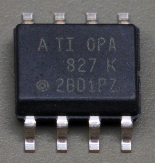
The Texas Instruments OPA827 is the successor to the well-known OPA627 precision opamp. At 22MHz, the cutoff frequency of the OPA827 is slightly higher than that of the OPA627. However, the maximum slewrate is slightly lower at 28V/µs. The offset voltage of the OPA827 is lower even without binning. The input noise has also been reduced slightly.
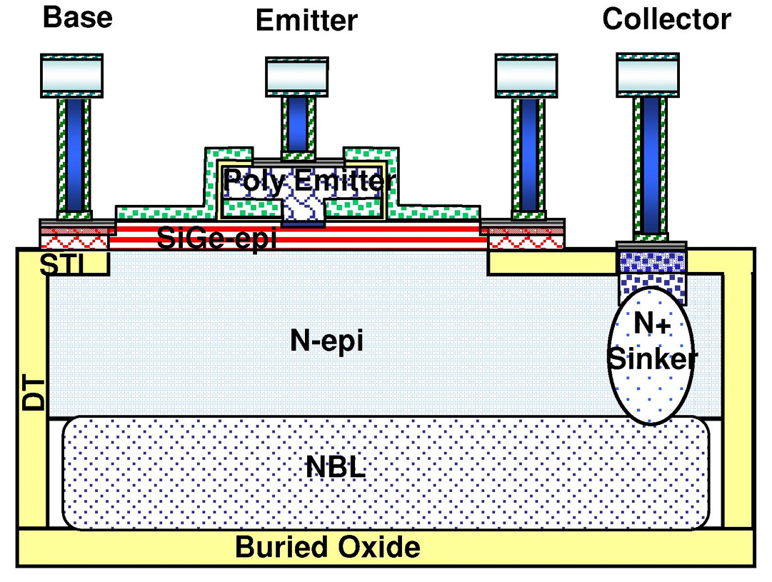


The January 2007 issue of New Electronics magazine features an article on the BiCom3HV process. It mentions the OPA827, which is also based on this process. Details on the BiCom3HV process can be found in the IEEE publication “BiCom3HV - A 36V Complementary SiGe Bipolar and JFET Technology.” The above sketch, which shows how an NPN transistor is constructed in this process, was also published there. These transistors block up to 40V. The use of SiGe also enables high switching frequencies. The transition frequency is up to 4,2GHz. This is an SOI (Silicon on Insulator) process, which means that the parasitic capacitances are largely independent of the applied voltage.
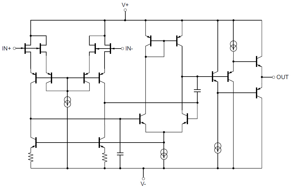


The datasheet contains a circuit diagram that is similar to the circuit diagram of the OPA627. The OPA627 had p-channel JFETs at the inputs. Here, there are n-channel JFETs that are directly connected to the positive supply. The additional input transistors were also present in the OPA627, but are not yet shown in the datasheet. With the TO-99 package, the OPA627 offers two additional contacts to adjust the current distribution in the current mirror and thus the offset voltage. This interface has been omitted in the OPA827.
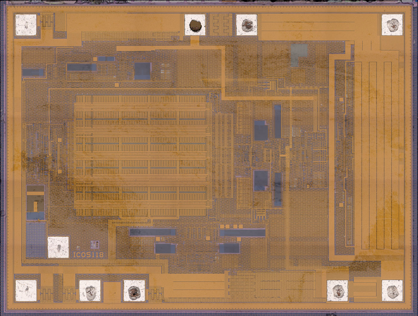


The dimensions of the die are 1,7mm x 1,3mm. It is therefore significantly smaller than the die in the OPA627 (2,9mm x 2,0mm). Most of the surface area has been filled with dummy structures. Nevertheless, the input transistors are clearly visible. Like the OPA627, the OPA827 also works with a large number of relatively large input transistors. The large surface area ensures low noise. The circuitry reduces offsets that could otherwise arise due to temperature gradients. In the top metal layer, the input transistor area is recognizable by its symmetrical, relatively wide lines. The two bondpads on the lower edge in the left area represent the inputs. The wide connections to the input transistors are clearly visible.

The output stage is located on the right edge. It stands out due to its even wider lines. The central placement ensures the most homogeneous temperature gradients possible in the input transistors. It appears that separate bondpads have been integrated to supply the output stage.

Three bondpads remain unconnected in the left-hand section. The bondpad located slightly further inside the die has no protective structures. This potential is probably only used for testing or calibration purposes. The two bondpads in the left-hand corners are equipped with protective structures. Perhaps an offset calibration could be performed on them, as with the OPA627.

This image is also available in higher resolution: https://www.richis-lab.de/images/Opamp/a15x03XL.jpg (92MB)
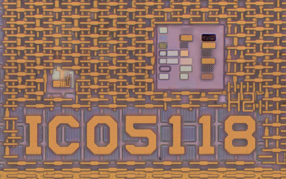


IC05118 appears to be the internal project designation. Rectangles have been drawn all over it in various places.


The die contains several laser-matched resistors, similar to those found in the OPA140, among others.

Also interesting are the interconnected squares above the resistor, which resemble fuses. These are certainly not fuses, as the passivation layer completely covers the structure. One can only assume that these are auxiliary structures that can be used during development or troubleshooting. In these situations, opening the passivation layer and modifying the metal layer is a reasonable effort.
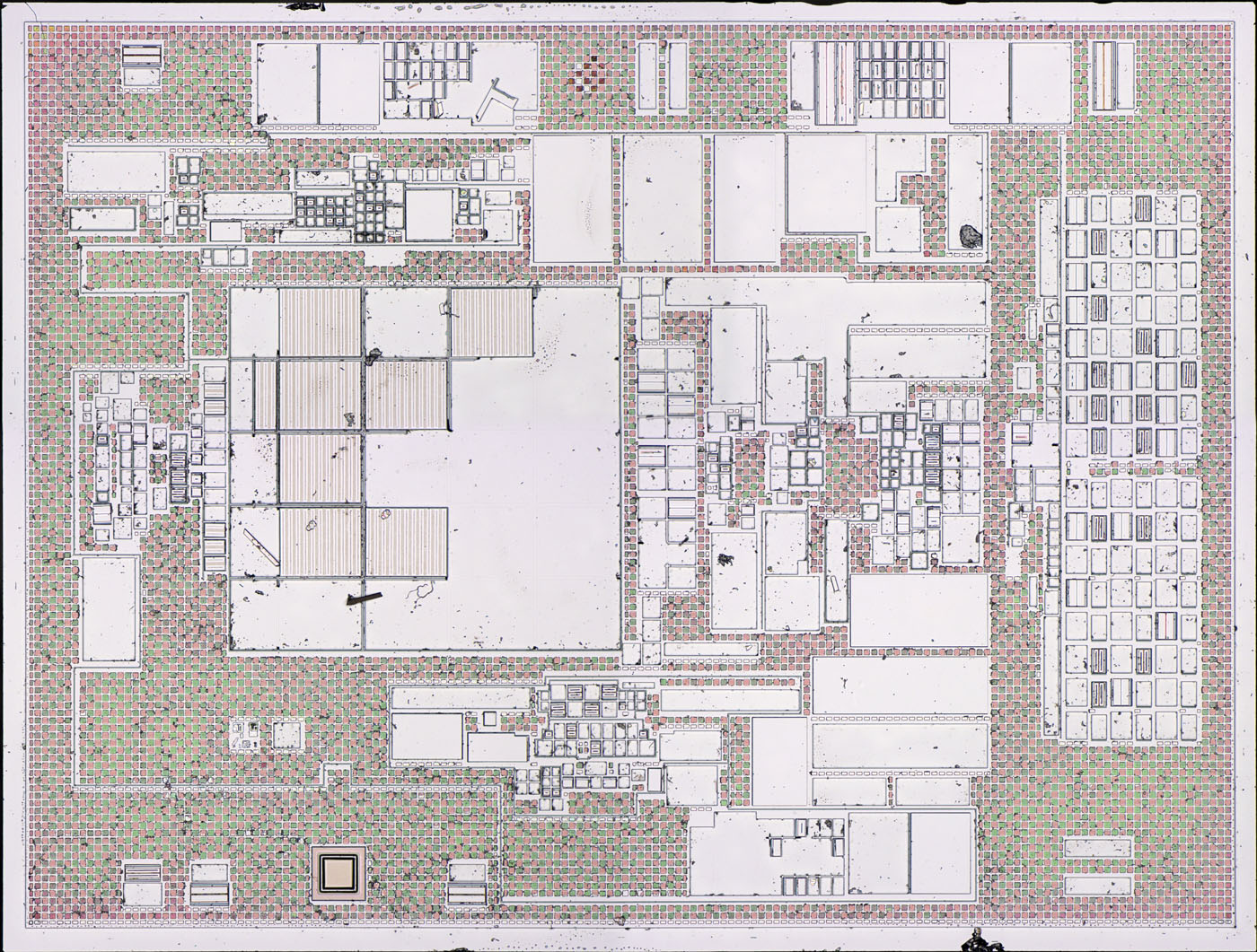


If the upper layers are removed, it becomes apparent that large areas do not contain any active elements.

This image is also available in a higher resolution: https://www.richis-lab.de/images/Opamp/a15x06XL.jpg (26MB)
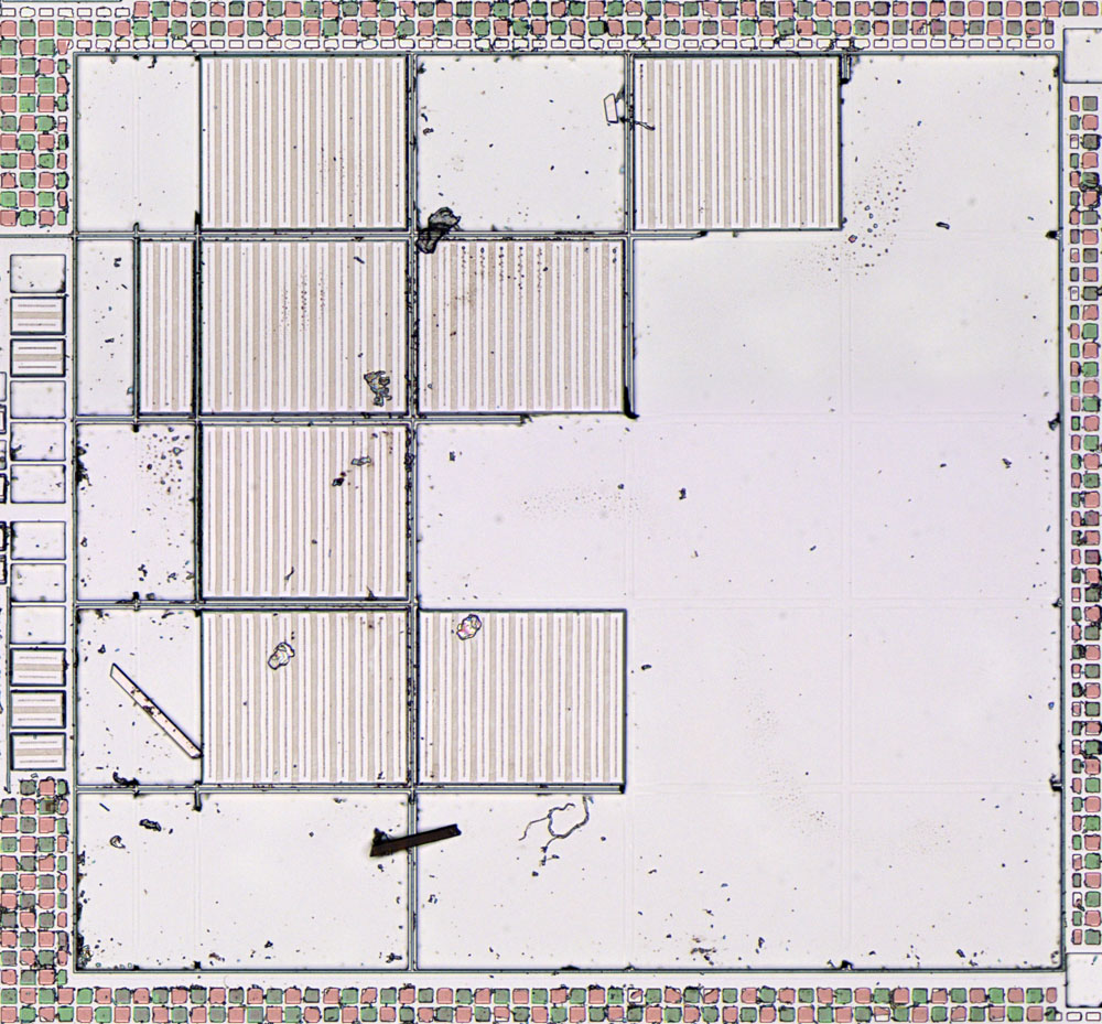


The lowest structures of the input transistors are still partially intact. There are 20 large and 8 small blocks.


https://www.richis-lab.de/OpampA10.htm

 :-/O
 
The following users thanked this post: RoGeorge, magic

Offline magic

  • Super Contributor
  • ***
  • Posts: 8063
  • Country: pl
Re: Opamps - Die pictures
« Reply #765 on: December 13, 2025, 07:51:56 am »
The datasheet contains a circuit diagram that is similar to the circuit diagram of the OPA627. The OPA627 had p-channel JFETs at the inputs. Here, there are n-channel JFETs that are directly connected to the positive supply.
I suspect they still use this drain bootstrap scheme. While SOI reduces gate-substrate capacitance, it does nothing to gate-drain. Moreover, gate-drain is a PN junction so the capacitance varies with common mode input voltage if the drain is fixed at V+. It's practically guaranteed that the drains are bootstrapped.

Like with OPA627, the schematic looks simple, but reality is a bit more complex. It's bummer that those new TI chips are hard to read.
 
The following users thanked this post: Noopy

Offline NoopyTopic starter

  • Super Contributor
  • ***
  • Posts: 2404
  • Country: de
    • Richis-Lab
Re: Opamps - Die pictures
« Reply #766 on: December 14, 2025, 03:56:40 am »
I agree with you.
But there are no numbers telling us how the input capacitances vary with the supply voltage. We don´t know what is happening there.
On the other side the input current is quite stable with varying common mode voltage. That would not be the case if there is a pn-junction between the inputs and V+.

Offline David Hess

  • Super Contributor
  • ***
  • Posts: 19218
  • Country: us
  • DavidH
Re: Opamps - Die pictures
« Reply #767 on: December 14, 2025, 05:23:40 am »
But there are no numbers telling us how the input capacitances vary with the supply voltage. We don´t know what is happening there.
On the other side the input current is quite stable with varying common mode voltage. That would not be the case if there is a pn-junction between the inputs and V+.

Wouldn't the input protection network be bootstrapped as well to control leakage and input capacitance variation?

Another thing not shown is bootstrapping of the JFETs.  At high drain voltage, that is starting as a few volts, impact ionization causes an increase in gate leakage.  It would not normally matter, but the specified input bias current is pretty low for a JFET.

It is too bad that the datasheet schematic is so sparse, but given that it is Texas Instruments, we are lucky to have anything at all.
« Last Edit: December 14, 2025, 05:27:39 am by David Hess »
 
The following users thanked this post: Noopy

Offline NoopyTopic starter

  • Super Contributor
  • ***
  • Posts: 2404
  • Country: de
    • Richis-Lab
Re: Opamps - Die pictures
« Reply #768 on: December 14, 2025, 07:29:58 am »
Wouldn't the input protection network be bootstrapped as well to control leakage and input capacitance variation?

Yes, probably.

It is too bad that the datasheet schematic is so sparse, but given that it is Texas Instruments, we are lucky to have anything at all.

Some day I will develop a proper delayering technology... But the OPA827 is too pricey to do a lot of destructive experiments.

Offline magic

  • Super Contributor
  • ***
  • Posts: 8063
  • Country: pl
Re: Opamps - Die pictures
« Reply #769 on: December 14, 2025, 08:08:11 am »
But there are no numbers telling us how the input capacitances vary with the supply voltage. We don´t know what is happening there.
On the other side the input current is quite stable with varying common mode voltage. That would not be the case if there is a pn-junction between the inputs and V+.

Wouldn't the input protection network be bootstrapped as well to control leakage and input capacitance variation?
That's a good question, but I'm not sure if the answer is yes. LMC660 has some of the lowest leakage out there and there was speculation that its ESD diodes are bootstrapped, but IIRC we found zero evidence of that. Maybe it helps that those diodes are much smaller than typical low noise input transistors.

It is too bad that the datasheet schematic is so sparse, but given that it is Texas Instruments, we are lucky to have anything at all.
They are getting there ;)


Some day I will develop a proper delayering technology... But the OPA827 is too pricey to do a lot of destructive experiments.
Since most of the problem is the sparse filler pattern, I wonder if it would work to "delayer" them with a low DOF objective?
 

Offline NoopyTopic starter

  • Super Contributor
  • ***
  • Posts: 2404
  • Country: de
    • Richis-Lab
Re: Opamps - Die pictures
« Reply #770 on: December 14, 2025, 08:30:53 am »
Since most of the problem is the sparse filler pattern, I wonder if it would work to "delayer" them with a low DOF objective?

Unfortunately that doesn´t really help. There is too much filler...

Online iMo

  • Super Contributor
  • ***
  • Posts: 6904
  • Country: li
Re: Opamps - Die pictures
« Reply #771 on: December 14, 2025, 09:01:23 am »
..when you download the pspice TI model of the OPA828 you get ~400lines long model.. perhaps it contains some useful info..
Readers discretion is advised..
 

Offline David Hess

  • Super Contributor
  • ***
  • Posts: 19218
  • Country: us
  • DavidH
Re: Opamps - Die pictures
« Reply #772 on: December 14, 2025, 06:14:41 pm »
It is too bad that the datasheet schematic is so sparse, but given that it is Texas Instruments, we are lucky to have anything at all.

They are getting there ;)

Usually they (Texas Instruments) just show nothing.

What is needed are details of the input and output circuits to properly gauge things like differential input voltage range, and direction of input bias current.

I got the feeling that companies like Linear Technology and Precision Monolithics Incorporated were formed by dissatisfied engineers who were not receiving proper credit for their work, but these companies also published much better datasheets, usually with detailed schematics.  Now with Analog Devices having purchased LT and PMI, and Texas Instruments having purchased BB and National, we seem to be heading back to the days of obfuscated datasheets.
« Last Edit: December 14, 2025, 06:18:43 pm by David Hess »
 
The following users thanked this post: exe

Online iMo

  • Super Contributor
  • ***
  • Posts: 6904
  • Country: li
Re: Opamps - Die pictures
« Reply #773 on: December 15, 2025, 10:23:03 am »
Those chips are commodity today and the companies wants to save $ where possible. Thus why to mess with such details.. Also the competitors are technologically much more capable than, say, 40-50y back, so why to feed them with implementation details?
 ::)

..Now with Analog Devices having purchased LT and PMI, and Texas Instruments having purchased BB and National, we seem to be heading back to the days of obfuscated datasheets.
« Last Edit: December 15, 2025, 10:24:44 am by iMo »
Readers discretion is advised..
 

Offline magic

  • Super Contributor
  • ***
  • Posts: 8063
  • Country: pl
Re: Opamps - Die pictures
« Reply #774 on: December 15, 2025, 12:57:29 pm »
IMO more likely that they want to be able to change things without telling anyone. Like swapping CMOS dice into TL072 :palm:

I'm sure competitors can reverse engineer this circuit topology easily. The only thing stopping me and Noopy is lack of process to strip those metal layers one by one. Older OPA627 or even LM4562 have one metal layer and I can produce full schematics of those. These TI chips aren't much denser, there is a limit to how small you can make a bipolar transistor running at 36V.
« Last Edit: December 15, 2025, 01:00:46 pm by magic »


Share me

Digg  Facebook  SlashDot  Delicious  Technorati  Twitter  Google  Yahoo
Smf


-->