-
Thank you, Le_Bassiste.
After reading your post I decided to put the instrument back together and test. I did not bother to put push rods back in, since I will be disassembling it again.
The good news is that it runs ok. On 10 volt range it is about 15ppm away from my 34401a. I measured a 10 Ohm standard and got 10.000065 - not too bad either.
The bad news is that after being assembled it repeatedly failed the self test with 306.2 error: 1.92?A ohms source. This corresponds to 2 MOhm range. This range was not working properly even before recapping.
I used 34401a to check the current on the 2 MOhm range and it was fluctuating wildly between 2.8?A and 4.0?A. Then all of the sudden it snapped to 1.90?A and became stable. I checked the resistance measurement in 2 MOhm range and it worked fine. Ran self tests and they all passed.
I power cycled the meter and again everything passed.
This situation with an intermittent current source problem has me completely at the loss. I would appreciate any troubleshooting ideas. Thanks.
-
Today I checked the base level noise and got 4uV. This did not improve after an hour of a warm up.
I used a copper strand with Q-tip to short the inputs. This seems too high.
My 34401a starts at 4uV but fairly quickly settles to 0.3uV.
Le_Bassiste, I think you reported something similar with your 2002. How did you get it resolved?
Is there something I can do to troubleshoot this? Thanks. -
Welcome to forums. K2002 is my second favourite meter
What would be your most favourite meter? .
.
-
Today I checked the base level noise and got 4uV. This did not improve after an hour of a warm up.
I used a copper strand with Q-tip to short the inputs. This seems too high.
not sure as to whether you are talking about "noise" or "offset" here, so i assume that you mean "offset"
after cold start, (instrument was off for 24 hrs) my specimen needs about 2.5 hrs to fully settle from approx. 6µV to some constant offset value (set to DC, 200mV, 10NPLCs, no FILT, input shorted).
i'm not concerned about the constant offset, as that will be fixed, once the instrumet has got a calibrate/adjust run in a cal lab. also, that constant offset value is "rock stable", i.e., even after a continuous run for a month, that offset didn't change at all (well, it did change with ambient temperature, but always came back to same value for same temperature).
but i am wondering whether the amount of initial drift of several µV has to be considered too high, and might point to some hidden fault. otoh, the instrument passes all self tests.
so, would be great if you could post some of your offset values wrt time here
as for "noise", have look here, where i posted some values that may be helpful for further performance verification of your 2002. note that i've used quite a small sample window of just 50 samples, so take them with a grain of salt. should be fine for a q&d performance check, though.
https://www.eevblog.com/forum/repair/keithley-2002-repair/msg1188312/#msg1188312
-
Thanks.
I checked the noise and so far it seems around +/- .5uV and the offset is around -4.2mV even after warmup.
I am still trying to troubleshoot 1.98uA source and currently suspecting problems with either Q244, Q242 or CR217. Do you know what parts they are? Here is a photo of one of them.
Also here is a thermal shot of the meter after warmup. Surprisingly ADC is very hot as well as area around 3 electrolytics by display board (they themselves are cold - cold horizontal line in the lower right corner)
Sent from my iPhone using Tapatalk -
Have you checked input leakage / bias in voltage mode ?
A jumpy test current could also be due to leakage at the input. The ohms current source is reasonably well protected and thus not that likely to show a defect. Input protection and switching is much more exposed to things like ESD. -
looking good. mine is around 3.4µV offset at 23°C, hovering about 40 nV/°C
I checked the noise and so far it seems around +/- .5uV and the offset is around -4.2mV even after warmup.I am still trying to troubleshoot 1.98uA source and currently suspecting problems with either Q244, Q242 or CR217. Do you know what parts they are? Here is a photo of one of them.
it's a siliconix J2611 JFET.
note colour dots on top. these are factory-selected and marked, so it might be better to not try and change/remove them, until you are absolutely sure that they've gone south.Also here is a thermal shot of the meter after warmup. Surprisingly ADC is very hot as well as area around 3 electrolytics by display board (they themselves are cold - cold horizontal line in the lower right corner)
on the ADC, the CPLD can get quite warm, no reason to worry. same holds true for the three electrolytics next to the smal silver box. the temperature of that box is actually very high, but its nickel plating is fooling your TIC into false temp readings (because emissivity of metallic platings is much lower than that of the other things around the box).
did you try to slightly(!) knock with a popsickle stick on the board? can that provoke a jumpy ohms reading?
are the current jumps still noticeable when measuring a resistor in non-auto-ranging mode?
(i must admit, a little bit poking in the dark here
EDIT: did you read this?
https://www.eevblog.com/forum/repair/keithley-2002-repair-help/25/#msg1227932 -
Have you checked input leakage / bias in voltage mode ?
A jumpy test current could also be due to leakage at the input. The ohms current source is reasonably well protected and thus not that likely to show a defect. Input protection and switching is much more exposed to things like ESD.
How do you check for input leakage?
Also, I am dealing with two separate issues, one is 4mV offset with shorted input and this might be normal.
Another is non working 2MOhms range (selected manually) and 306.2 error. The current source sometimes is at 1.98uA and is stable as it should be and sometimes is as high as 7.9uA and floating up and down by a lot.
Sent from my iPhone using Tapatalk -
did you try to slightly(!) knock with a popsickle stick on the board? can that provoke a jumpy ohms reading?
are the current jumps still noticeable when measuring a resistor in non-auto-ranging mode?
I manually set 2MOhms range. While in this range sometimes current jumps and someones is it stable. I have seen it change both ways without any mechanical interaction on my part. I will watch it a bit more. It almost seems thermal rather than mechanical. However I will try the knocking test tonight.
it's a siliconix J2611 JFET.
note colour dots on top. these are factory-selected and marked, so it might be better to not try and change/remove them, until you are absolutely sure that they've gone south.
Thank you, yes I do see the yellow mark. Actually on Q242 and Q244. Now that I know they are JFETs they are less of a suspect.
Here is my test setup: I put the K2002 into 2Wire Ohms on 2MOhm range. I use Fluke 187-II in micro current mode (100 Ohm impedance) to measure current produced by K2002 between Input High and Input Low. K2002 shows 0.000100MOhm when working well or higher number when not. While monitoring the current, I use 34401a to measure voltages relative to Input Low of K2002.
One noticeable difference is on CR217. When working well one leg is at 304.3mV and another at 0.64mV and fairly stable. When not working properly one leg is still at around 300mV but fluctuates a bit, while another is at 1.5mV and fluctuates a lot.
Also, when working well very stable 12.7017 is seen on legs on Q211 and Q212 and in contrast when misbehaving I can see around 9v on these legs and it fluctuates a lot.
It would be much easier if I had schematics. Any help is appreciated. Thank you.
-
The changing voltages around Q211, Q212 might be a clue to the issue. However without a schematics, it is not that easy. There is a reverse engineered schematics for the ADC part around. Chances are the input stage is somewhat similar to the K2001.
Measuring leakage / input current is relatively easy. There are two options:
1) use a 10 M or similar resistor across the inputs in the volts (e.g. 2 V) range.
2) have a low leakage capacitor (e.g. 1 nF) across the inputs an watch is charging / discharging. -
Measuring leakage / input current is relatively easy. There are two options:
1) use a 10 M or similar resistor across the inputs in the volts (e.g. 2 V) range.
2) have a low leakage capacitor (e.g. 1 nF) across the inputs an watch is charging / discharging.
1) 10M standard resistor on 2V scale is giving me around 60uV if I stay 3 meters away and stay very still.
2) I did not have a 1nF capacitor handy, so in a pinch I used 200nF GenRad 1409 capacitance standard. It showed about 1.4V and was discharging approximately at .1mV per second.
Is this good?did you try to slightly(!) knock with a popsickle stick on the board? can that provoke a jumpy ohms reading?
Mechanical knocking on the board does not change a thing.
I am planning to do some offset voltage plotting after I get GPIB connection working.
The search continues...
Is there a way to test Q211, Q212 and Q213 in circuit? I do not want to desolder them unless I have to.
-
60 µV at 10 M is only 6 pA. 0.1 mV/s for a 200 nF capacitor would be 20 pA - this includes capacitor leakage and maybe dielectric absorbtion.
So leakage seems to be very low - usual specs are something like below 50 pA.
Checking JFETs in circuit could be difficult - the error still seems to be more intermittent or just marginal. So one would not a expect a fully broken part, but more like a parameter shift, excess leakage or unwanted oscillation. This might be even hard to detect on a separate part.
It might be worth checking the drive signals, that control the JFETs - there have been faults in the LM339 chips and even the shift registers used for control. The fluctuating state might also be due to oscillation - so maybe time to use a scope.
It might also help to get at least a crude schematics of the suspected area. From TiN's tear-down the circuit seems to be similar to the K2001 meter for which schematics are available.
-
Thank you fro validating leakage spec.
I really like the suggestion to use scope. This will be my next thing to do.
So far I validated R322, CR217, K201, R334 and R342 (parallel to L206). I used every resistor in the chain as if it would be a current sense resistor, to make sure it is about the same wrong current going through all of them, when device is misbehaving.
I doubt it is the return circuit responsible for the issue (Q246, Q245, Q244, and Q242).
So I am left with everything prior to R322 to look for problem.
The repair manual is referring to /OHMD line, OHMREFHI and REFBUF. What are they? Thanks.
-
There is quite some description in the repair manual:
The /OHMD signal is a digital control signal to set the current source to 2 µA. Due to the / in the name, likely active low. OHMREFHI and REFBUF are a 14 V signal and a buffered 7 V reference.
The 9.6 µA and 2 µA current source seem to use many of the same parts. So one might exclude those used for the 9.6 µA current source. The change from 9.6 µA to 2 µA seems to be changing the reference voltages - thus not in the super higher impedance part. My suspect would be more like U232. It would be really worth checking those ref voltages used for the current source. It may help to make a drawing of the current source - there is quite some descriptions to help with this. However it seems to be a little different from the K2001. -
The 9.6 µA and 2 µA current source seem to use many of the same parts. So one might exclude those used for the 9.6 µA current source. The change from 9.6 µA to 2 µA seems to be changing the reference voltages - thus not in the super higher impedance part. My suspect would be more like U232.
You are right on the money! When I checked U232 I discovered that when meter is properly producing 1.98uA in 2MOhm range, on U232 I get:
Pin 9: Low
Pin 10: 12.7175
Pin 11: 12.7154
Basically, Pin 10 connected to Pin 11, as they should.
When current is misbehaving, I get:
Pin 9: Low
Pin 10: 12.7175
Pin 11: FLOATING!!!!
To me it is a clear proof of U232 fault. Thank you, thank you, thank you!
Additionally, I checked U221 register that according to manual supped to be: 11101001, but in my case is 11101011 regardless of meter working properly or not (Bit 2 is different). It is possible that my firmware is too old and manual was based on new firmware.
Also in checking the repair manual in details, I found surprising number of inaccuracies, like U232 is listed as "CENTRIGRADE TEMP SENSOR LN35DM", instead of "IC SWITCH QUAD SPST 16SOIC". -
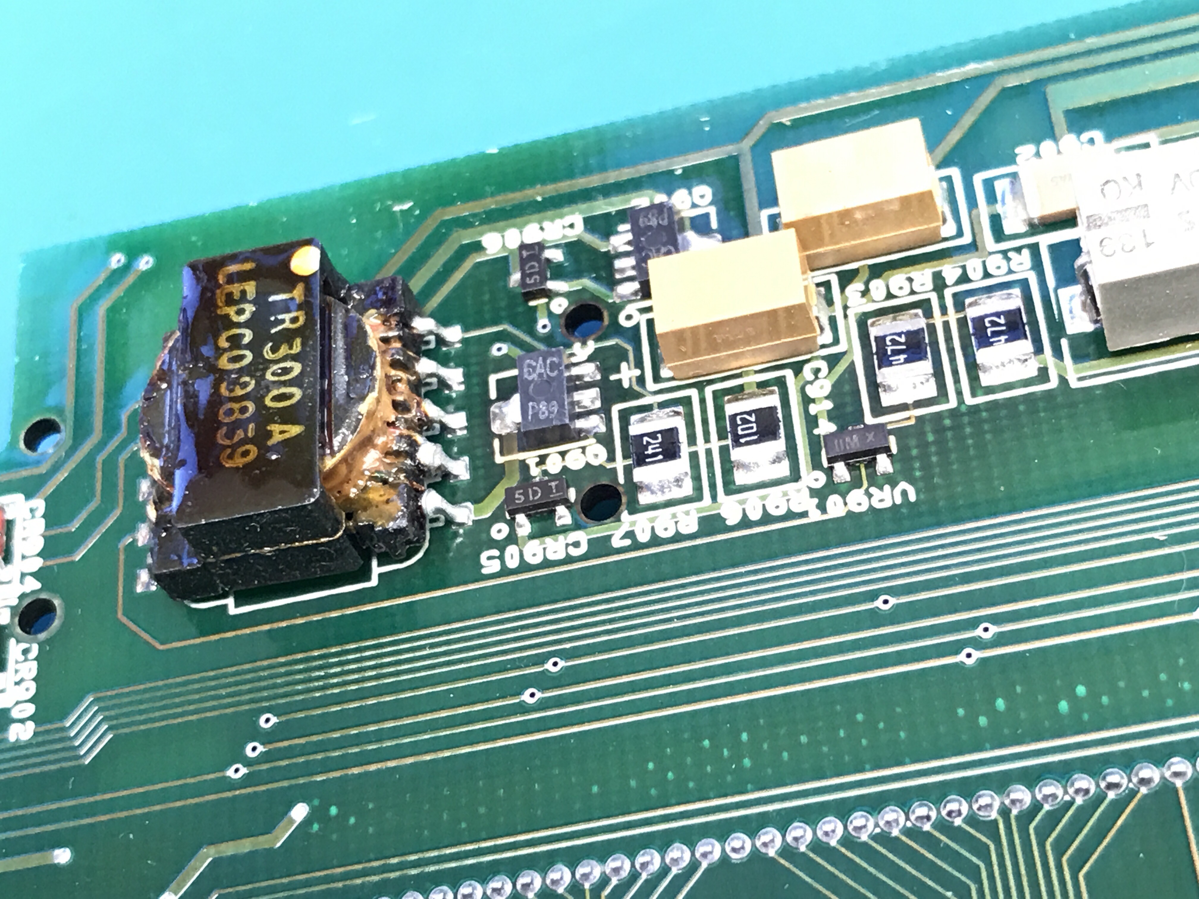
Now that I am on the way of fixing the 2MOhm range and waiting for parts, I am looking for the reason for overheating front panel.
hmm, after another look at your photos, i now see that it is not the transformer that caused the brown spot on the pcb,
 it's one of the two push-pull transistors on the primary side.
given the age of the instrument and the fact that the supply of the display is still giving the right voltages for filament and anode, you probably shouldn't be too worried about it.
the only thing that you could do is to exchange the transistors with some better ones. don't know from top of my head whether these are BJTs or MOSFETs, have a look at the KEI2001 schematics (VFD supply should be same as in KEI2002, but is located on digital board) on TiN's site to find out.
I took an infrared image of the front panel after the meter was on for a while and it shows very noticeable overheating in the same area where the board is discolored. See attached IR photo.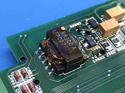

I do not have a high resolution thermal imager, so the photos are somewhat blurry. Nonetheless I can see that the VFD transformer gets hot, but only to 60C; At the same time 5 transistors in the vicinity and 4 somewhat large 1/4W resistors get to about 80C. This is with the panel open i.e. some ventilation. The temperature is probably much worse when panel is closed. In overall thermal shot of the front panel I can see the temperature bleeding into area of banana terminals and can attribute to EMF voltages.
I checked resistors and they have proper values and 4.7k resistors had a voltage drop of 31V DC, corresponding to dissipating 200mW for a resistor specked at 250mW. Maybe what I have is completely normal.
Can someone please take a thermal photo of the front panel of K2002 after it had been running for a whole? No opening of the unit required. Thanks.
-
Tomorrow will make thermal images, going to calibrate some agilent 34401a DMMs.
-
Now that I am on the way of fixing the 2MOhm range and waiting for parts, I am looking for the reason for overheating front panel.
I took an infrared image of the front panel after the meter was on for a while and it shows very noticeable overheating in the same area where the board is discolored. See attached IR photo.
I do not have a high resolution thermal imager, so the photos are somewhat blurry. Nonetheless I can see that the VFD transformer gets hot, but only to 60C; At the same time 5 transistors in the vicinity and 4 somewhat large 1/4W resistors get to about 80C. This is with the panel open i.e. some ventilation. The temperature is probably much worse when panel is closed. In overall thermal shot of the front panel I can see the temperature bleeding into area of banana terminals and can attribute to EMF voltages.
Can someone please take a thermal photo of the front panel of K2002 after it had been running for a whole? No opening of the unit required. Thanks.
here you go: my 2002 after approx. 120 hours uptime, sitting between a cooking 2001 and a reference box, ambient at 30°C
-
Le_Bassiste,
Thank you for posting. Your meter shows 22C degree rise over ambient (great point to bring ambient temperature into this).
I was getting 41C max with ambient at 22C to amount to 19C rise over ambient. Give or take the same result as yours.
My heat center is also exactly at the same spot as yours. It looks like it is not the transformer but resistors and transistors that heat up the most.
This is bound to create temperature differential in connectors. How could this be on such a precision instrument?
Do I now have to use low EMF cables?
Samagon,
Can you please upload your thermal photo? -
I agree that for a precision instrument so much heat is not a good idea. But on the other side low noise amplifiers need a certain current and thus generate heat. The heat is one reason I do not like the rather power hungry VFD or even Nixi displays. So a simple B&W LCD also has advantages.
Still I don't see a need for the power supply here likely the driver for the small transformer needs to get so hot. At least today there should be more efficient DCDC converters - even if it has to be low noise / low EMI. It looks like the transistor is the main heat source - except in a linear supply this should not happen so much. The temperature really seems to be on the high side - the discoloration of the board is not a good sign, even if this might have happened in a hot environment. So there might be a fault causing too high a consumption.
However the main heat is not so much near the terminals, but more to the other side. Just plain copper wires are already not that bad with thermal EMF. This is also just a regular DMM, not a nV or special low level meter. -
Here it is, after approx 1 hour of warm up.
Ambient temp 24C
-
Here it is, after approx 1 hour of warm up.
Ambient temp 24C
Also a 20C rise in temperature and the same spot! Thank you very much.
I guess there is nothing wrong with temperature rise on my K2002... Great news after all.
-
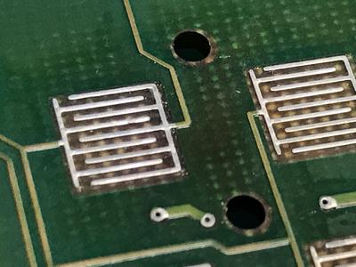
Parts arrived. I am looking at replacing U232 and desoldering it looks a bit daunting with guard traces and precision resistors in a close proximity:

Using fan is out of the question because of thermal concern for resistors. I am considering an enamel wire to bend legs up one by one, as I am desoldering them. And also use of no-clean RMA flux, because I will not be able to clean under microchip after soldering replacement.
Any suggestions for a proper procedure?
How about not desoldering the microchip at all, but just adding a new one on the top of non working chip? It is just an analog switch and the only fault is that one channel sometimes does not turn on completely.... Would that be too crazy?
Sent from my iPhone using Tapatalk -
Just cut legs off. No heat, no contamination.
-
Just cut legs off. No heat, no contamination.
Sounds brutal, but effective
Almost like quote from a mafia movie: "oh, just cut the legs off"
All joking aside I was afraid of leg moving enough from just being cut and damaging the pad. I practiced on two throw away SOIC 16 chips and the procedure worked like a charm.
Thank you, Samogon.
Sent from my iPhone using Tapatalk