-
Suggestion: Never use ultrasonic bath on assembled PCB.
This will probably kill many/most of the semiconductors.
Hi Doctor Frank, do you have any example of that?
I fully agree with you for MEMS devices...
After some googleing:
https://electronics.stackexchange.com/questions/196373/components-to-avoid-using-on-an-ultrasonic-cleaner
Interesting, did not know that...
-
I would at least be careful with older chips that have unsupported bond wires (the ones with a lid on it and an open air die).
I don't know wether gold has an endurance limit, but aluminium doesn't have one, thereby aluminium foil is "eaten" by ultrasonic cleaners
https://youtu.be/YR5PgwEDFzs?t=2m20s
https://en.wikipedia.org/wiki/Fatigue_limit
-
That is some fascinating information. I did not expect ultrasonic cleaner to be able to damage the board.
Parts should be arriving today. I cannot wait to dig into this new project.
Sent from my iPhone using Tapatalk -
Zucca,
From the link you providedQuoteUltrasonic cleaning is fairly commonly used for cleaning flux from PCBs during the production process. I think you're assuming the wrong reason for their use in your answer.
But k2002 is not where i will use it.
And its pcb pretty big Crest ultra sonic cleaner of such size would cost ~$2k -
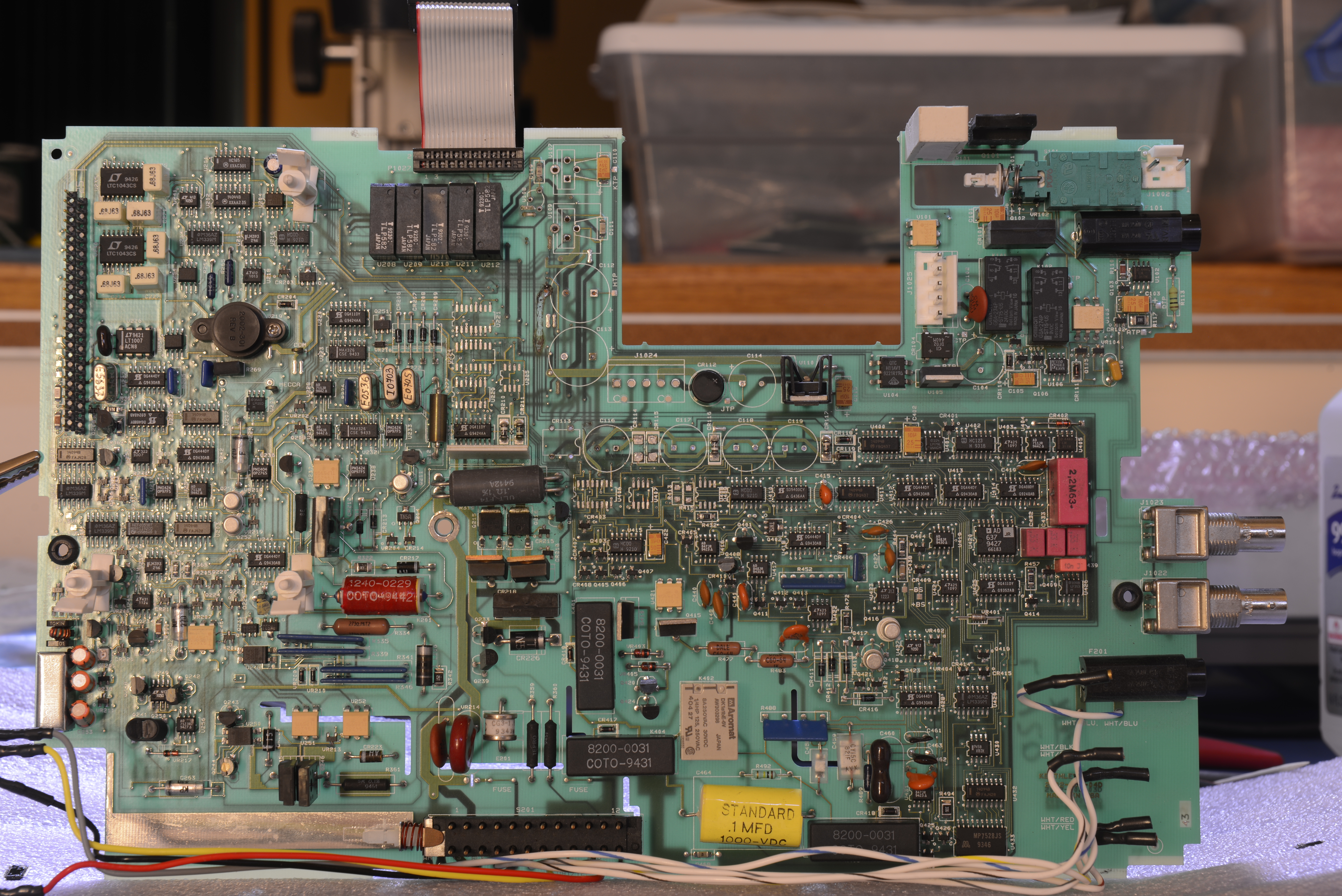
Picked up Keithley 2002 rejected from the calibration lab. They said that it would not hold DC Volts calibration. They gave me printout with DC Volts measurements they did using Fluke 5720 and on my my 10V standard I got the same reading give or take 0.5ppm. So I decided that my standard is not that bad.
I did the spot DC calibration myself. The meter asked me for 2V and 20V inputs and also dead short calibration. The short calibration took a very long time. Maybe 20 minutes or so. I did it with fluke's 88X-Short that looks identical to Keithley 8610. When I plug it in value fluctuate between 20nV and 180nV. I hope that is normal.
After that spot calibration unit is holding 2v, 20v, and 200v ranges very well (even after power down), so clearly EEPROM works. 200mV range is a bit off (by 10ppm or so) but this is only according to Keithley 2000, so I am not sure is that is an issue.
What else could be a reason for meter failing to calibrate at the lab?
Should I try comprehensive calibration myself before getting it back to the lab?
Thanks.
-
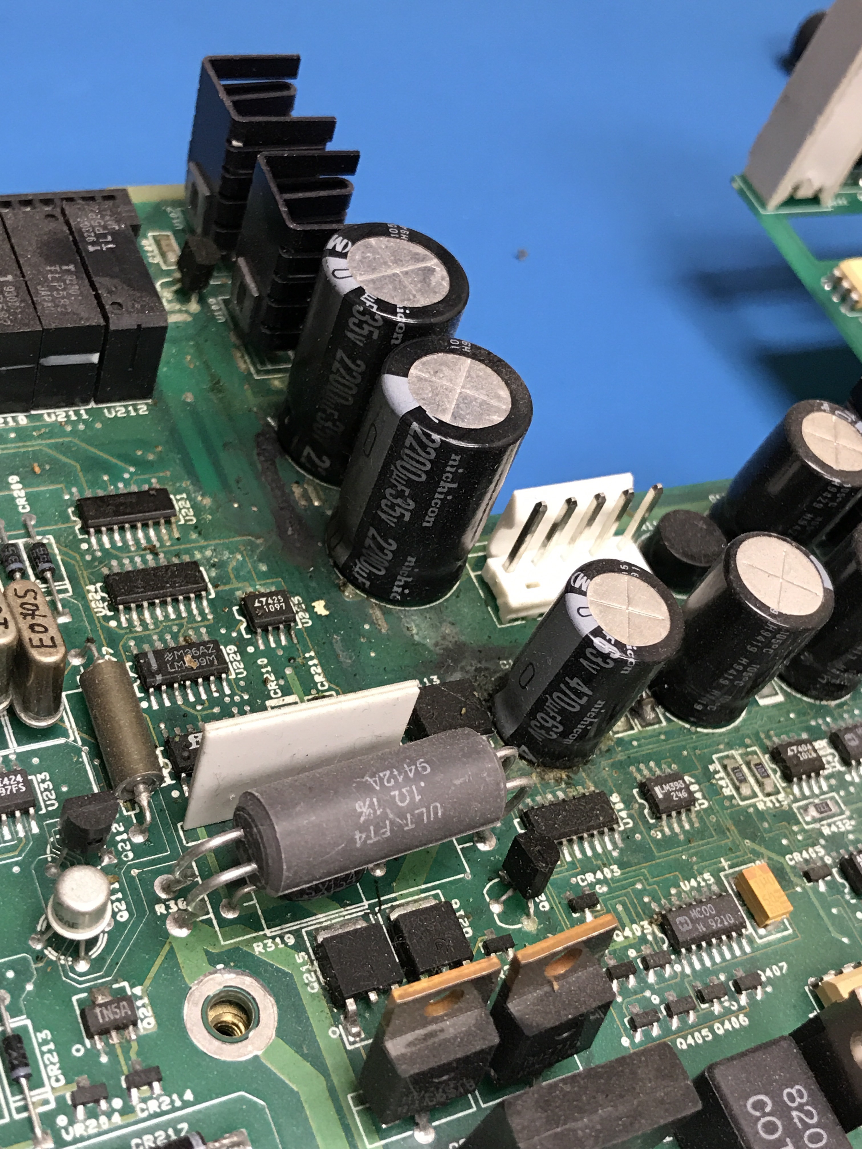
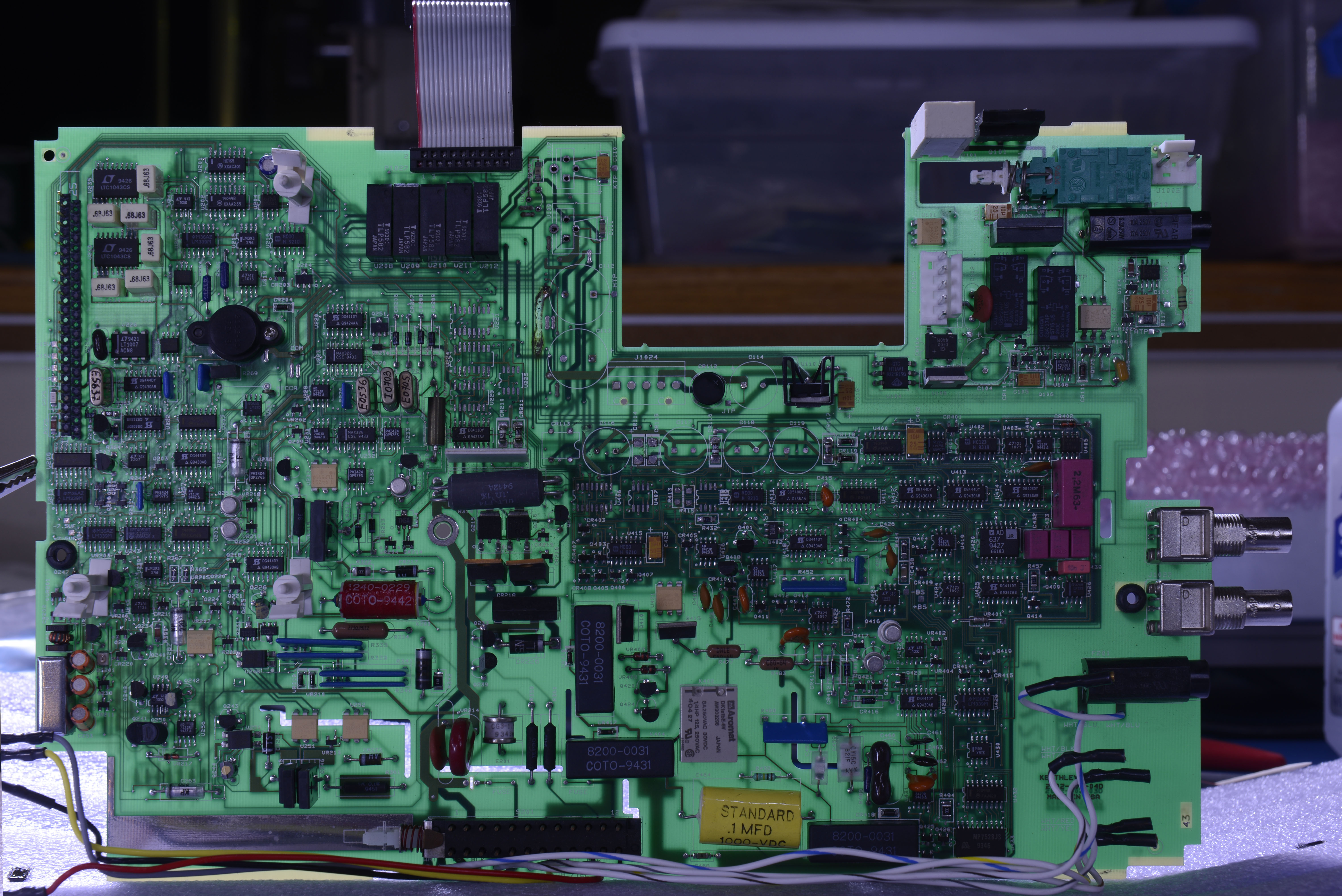
In a form of a short update, I finally had a bit of time to take the new (burned) K2002 apart.
I removed capacitors and diode bridge around burned spots. One capacitor blew a hole in its side while another leaked from the bottom. Basically a poster project on why you need to change capacitors in this.
As a result, there is one surface trace that was eaten - no big deal, one via that looks burned - no problem. And then a large burn through the board. It is basically ok on the bottom and a large extended black hole on the top.
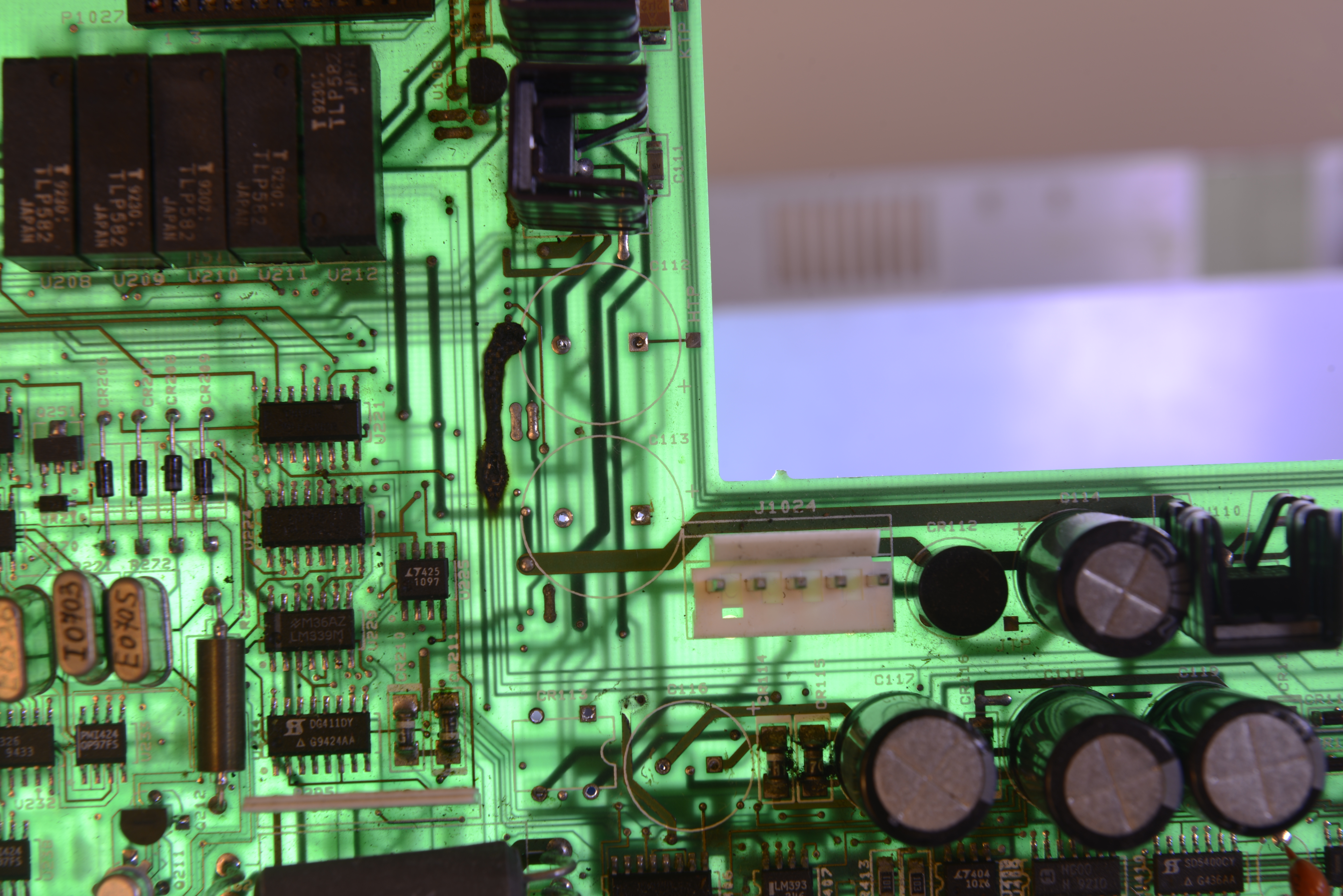
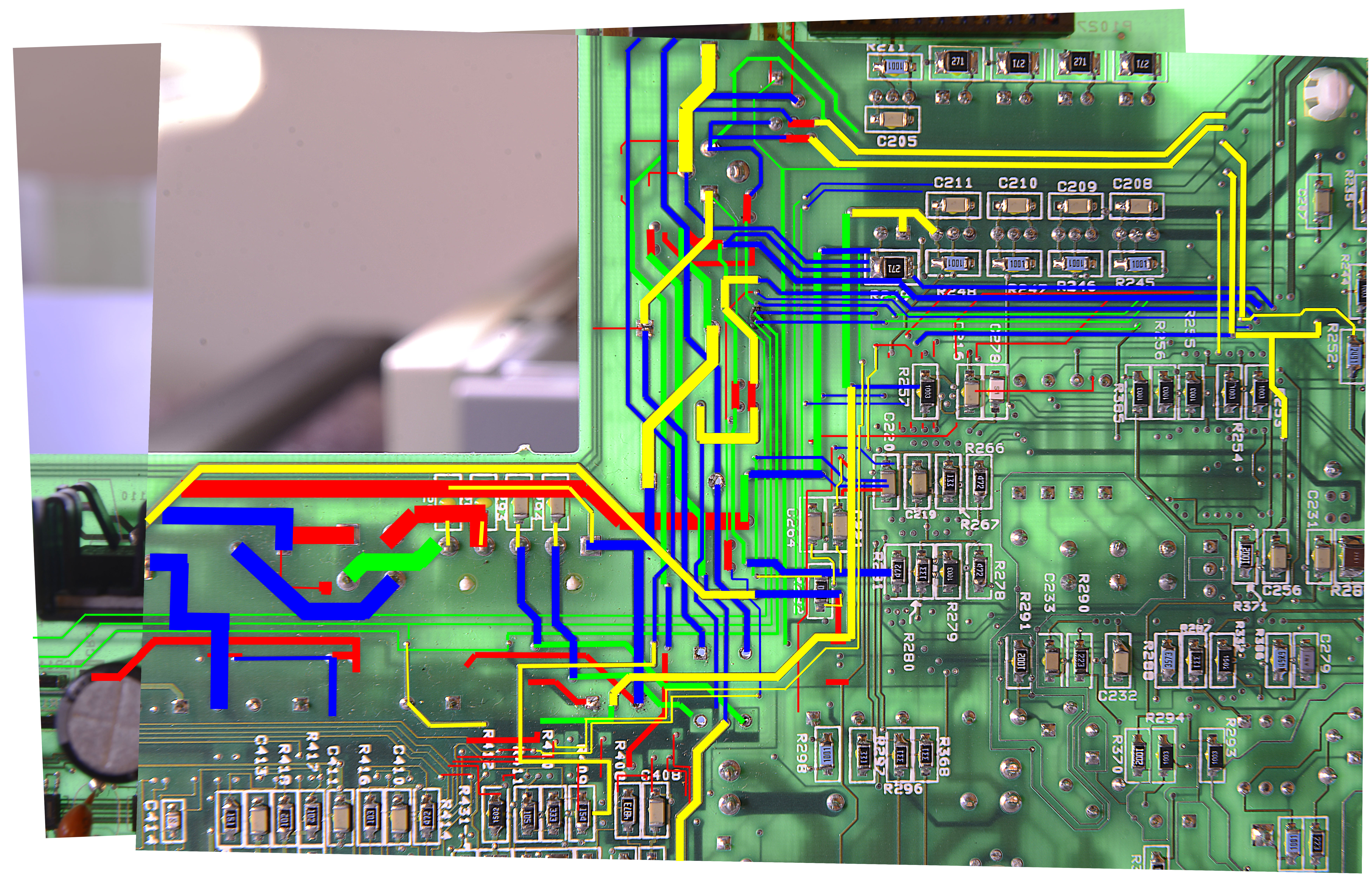
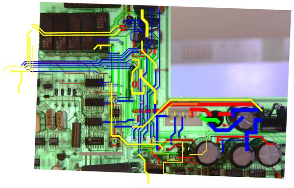
In attempt to understand the damage I "x-rayed" the board with a flashlight. Then I superimposed top and bottom view in photoshop and traced all the relevant conductors in 4 colors.
Red, Green, Blue and Yellow for all 4 layers of the PCB, with Red being component layer and blue and green two internal layers.
It appears that burned area did not have other top or bottom conductors. What got taken out is 3 internal conductors and 3 vias getting from layer 2 to 3.
Unfortunately as you can see all 3 traces start and end outside of area that I have reverse engineered. They probably are not even a part of power supply.
I will have to do more tracing work just to understand what these traces are.
More photos are coming. Wish me luck.
Sent from my iPhone using Tapatalk -
I don't miss this
 . Keithley 2001/2 are great for learning how to decipher cryptic layout. Often I had situation when trace goes under 1206 resistor/cap, and going out from the other side. You think, easy, same trace between the pads, right? Mhm, not quite ,there are two vias hidden under the thing.
Luck will not help here, but dedication and xxx amount of hours and late nights will do Looking forward for your fixes. 
My take would be to cut whole charred area and air-wire all connections with copper thin wire. You don't want leakage (burnt PCB is conductive carbon) to give you horrors. -
nikonoid I hope you will fix it. It´s so inspiring what you are doing...
-
I agree that you are going to have to dremel out all the burnt fiberglass...what a task you have set yourself
-
I am actually considering very small drill first and then needle file by hand, as there are many good traces nearby.
Sent from my iPhone using Tapatalk -
If the burnt part is only on one side of the board, one may not need a full hole in this area. If can be enough to remove the two burned layers for the one side. One could use something like a Dremel tool, or just scraping by hand with a knife.
It looks like there are 3 lines from below in the burned area, and nothing to the right. Likely there are good quality pictures on the xdevs site so one could get an idea where those lines are heading. -
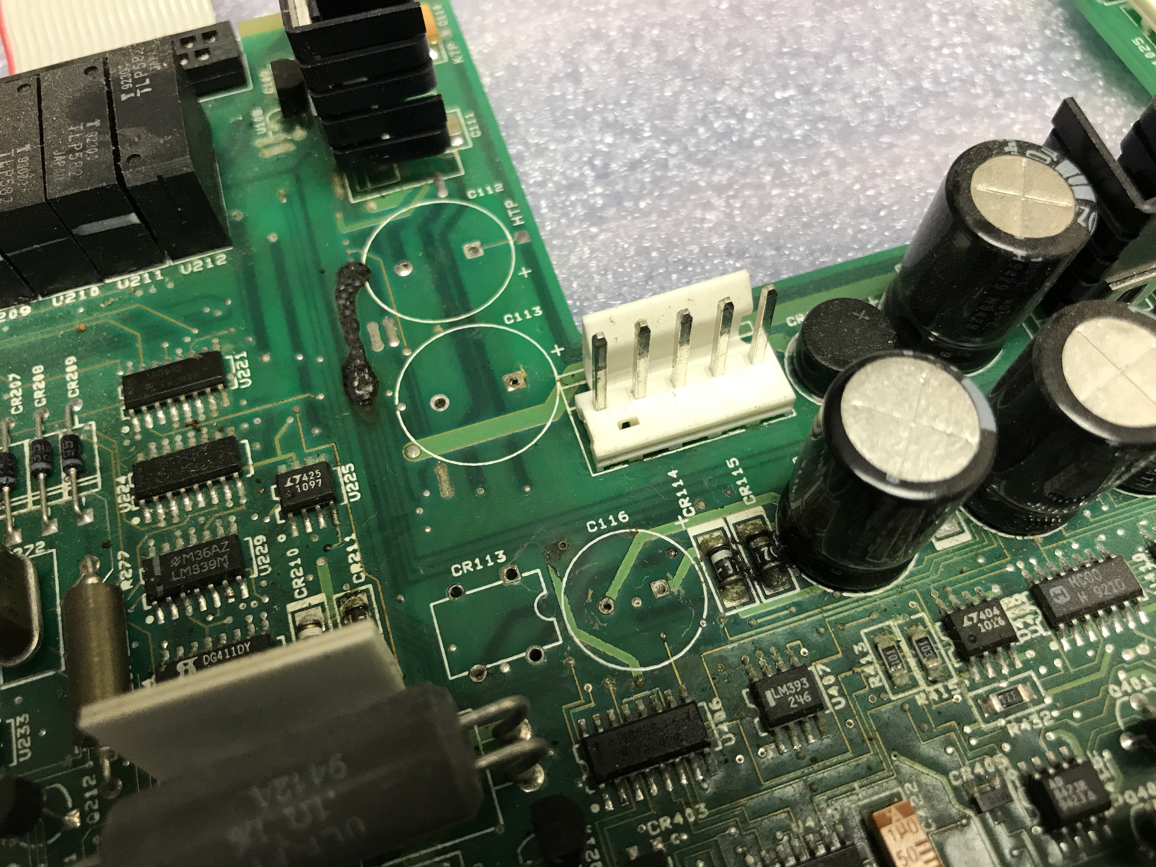
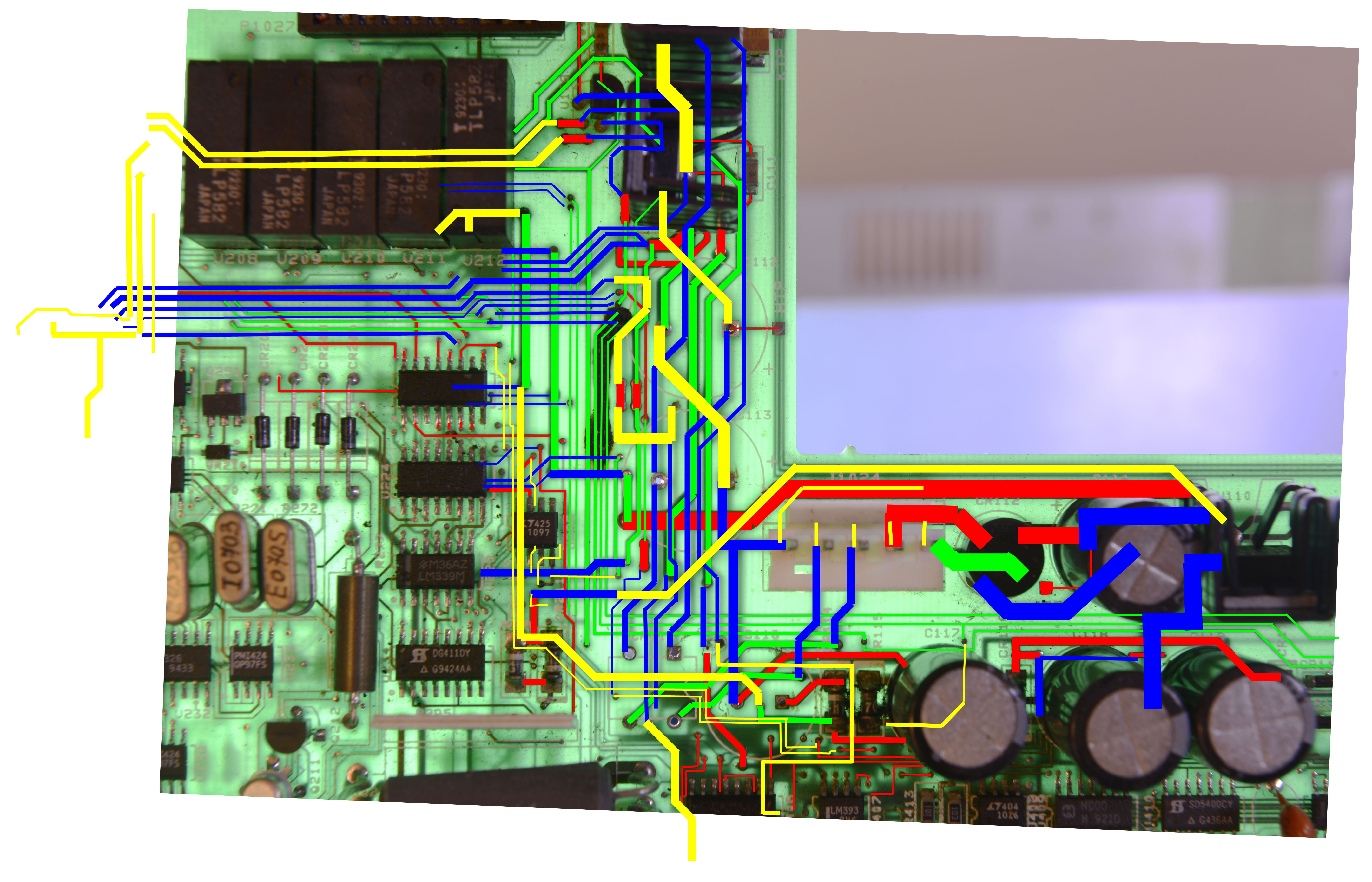
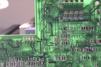
Best pic I had of that area is this one. Didn't take more photos of analog section, as there was nothing wrong on my second 2002 in there.
Also suggest not to take shortcuts and desolder all SMD parts in affected by electrolyte leak area (and replace cheap ones with brand new stuff), instead of thinking that little IPA and brush is enough. -
This is a great photo. Thank you, TiN. I can clearly see here layer 2 and what connects to what. Big help.
Sent from my iPhone using Tapatalk -
Today I found a second contributing factor to condition of the meter. Someone installed a 2 amp mains fuse instead of 1/2 amp. So one short happened due to electrolyte leak, it kept burning the board.
I started cleanup of the PCB burn. Made a decision against using dremel. I decided that any power tool throwing tiny conductive particles all over analog board is not a good thing . Arming myself with a wooden toothpick and 40x microscope, I removed as much of charred PCB as possible, periodically cleaning fine debris with IPA and Q-tips. After that came 1/16 drill bit in a Pin Vise (driven by hand) where some damage was drilled through and some scraped. Then I finished with an exacto knife. I am still debating with myself if I will remove more material.
I am potentially looking at making 5-7 bodge connections using thin transformer wire. Many of them will be soldered to tiny vias connecting 2nd and 3rd layers, showing on the surface only as a tiny dot. Is this an Ok thing to do or should I opt for much longer budge wire so I can solder it to more reliable spots?
Looking at the board under microscope proved that you guys are right again. I can clearly see electrolyte damage on some chips and traces. I will have to remove at least 7 ICs. Last time when I decided to cut legs of a microchip it worked, but less than perfectly. I am considering a using a soldering fan, covering nearby areas with either kapton film or aluminum foil for heat protection. Are there reasons not to do this and use some other technique?
Meanwhile here is more high res photos. This is the initial stage:
And this is after removing leaked capacitors and rectifier and a bit of cleaning:
I am still working on 4 layer PCB diagram on this section. I will post it soon. To create this diagram I took few photos on the PCB with light shining through it to help me see internal traces.
-
I wouldn't be cutting the legs of SOIC packages to remove them - IMHO that is a pretty bad way to do it. I much prefer to put a bunch of solder down the pins on one side, then lift it a little with a sharp knife. Then add some solder to the other side, grab the part with some tweezers and touch both sides back and forth and it should lift right off. With a little experience it is very quick. You can use the soldering iron to wick away most of the left over solder and then finish the cleaning with some wick, then alcohol.
Keithley PCB's aren't top quality but they aren't terrible either. -
Thank you, Steve.
I will give it a try. I have plenty of boards to practice on. What tip temperature would you suggest?I much prefer to put a bunch of solder down the pins on one side, then lift it a little with a sharp knife. Then add some solder to the other side, grab the part with some tweezers and touch both sides back and forth and it should lift right off. With a little experience it is very quick. You can use the soldering iron to wick away most of the left over solder and then finish the cleaning with some wick, then alcohol.
-
TheSteve,
I got a chance to try a method you recommended. It is a bit nerve racking to have a bunch of molten solder on the board. I had to get my tip temperature to 550F - this was the lowest temperature that would keep the solder molten when you go back and forth with iron. Hopefully the board is ok.
In the end I modified your process a bit, I would lift one side a little bit, then use desoldering iron with suction to remove solder still connecting lifted left to PCB and only then I would use extra solder on another half with tweeters to remove the chip.
This also gave me another proof that replacing components compromised with electrolyte is a must. Some microchips I was desoldering were corroded to the point that solder would not want to stick to them even with a good amount of flux.
Thanks again, 7 ICs are off the board now. Inspection under microscope showed no lifted of damaged pads.
I have another round of cleaning, then fixing broken lines and replacing parts. Unfortunately some of the parts are not arriving until the next week.
Meanwhile I called Keithley where I learned that top shield for 2002 is a non-orderable part - only internal technicians can order it. I can order top shield for Keithley 2001 and it is $55. Would someone know if top shields for 2001 and 2002 are somewhat compatible? Can I modify one into another?
-
Okay, you hit two no-no's in my book there.
If you have to increase tip temperature over 240-255C, that is a sign that tip and/or iron you using are not fit for the job. Meaning that PCBA is dissipating more heat than you providing. That means two things : you need larger surface area (bigger solder ball blob or wider more massive tip) or heatflow is not enough (need higher power soldering iron). Raising temperature might look like it's working ok, but you just delaminating PCB. Keithley analog PCB not good to survive high temperature, and those thin pads are easy to peel off. So work on your thermals
Second - pulling SOIC by one side is just making pads even more easy to damage. Keithley PCB have nSMD pads, usually connected just by thin trace without teardrops. I had number of times when pad and trace looked fine even under microscope, but actually were broken apart right at the point where pad connected to the trace. Searching for such faults wasted lot of hours.
After I started using only dual side SOIC heating, never have this issue again. Wide 4mm+ chisel tip with large solderblob flowing back and forth on both sides of IC works great. I'm using 120W handpiece to ensure good heatflow.
Top shield is same on 2001 and 2002, but there are two versions if them. One with cutout and duct for fan, and older one without cutouts, sealed type. If I remember correctly, they even have same partnumber. So I'd just order 2001 shields and be done with it. Make sure you order both top and bottom parts, and don't forget the mounting screw! It's not included with the cover. 
-
A different iron is needed if you need to turn the temp up like TiN posted. With the right tools and some experience it is a very quick process and will never cause any PCB damage.
And Keithley PCB's are pretty crap quality... -
If you have to increase tip temperature over 240-255C, that is a sign that tip and/or iron you using are not fit for the job. Meaning that PCBA is dissipating more heat than you providing. That means two things : you need larger surface area (bigger solder ball blob or wider more massive tip) or heatflow is not enough (need higher power soldering iron). Raising temperature might look like it's working ok, but you just delaminating PCB. Keithley analog PCB not good to survive high temperature, and those thin pads are easy to peel off. So work on your thermals
TiN, I think I just got lucky on thermals. Seeing your email I went to measure the tip with thermocouple. I loaded the tip with lots of solder for better contact. Two different thermocouples I have gave me 241C and 256C, when iron was showing 550F (288C). I am guessing my iron needs to be calibrated.
I use Hakko 888D with 2mm chisel tip and I like it. Should I consider Hakko 951 or something else?Second - pulling SOIC by one side is just making pads even more easy to damage. Keithley PCB have nSMD pads, usually connected just by thin trace without teardrops. I had number of times when pad and trace looked fine even under microscope, but actually were broken apart right at the point where pad connected to the trace. Searching for such faults wasted lot of hours.
Just in case I will do a very careful inspection of pads after cleaning and recheck vias in the area.Top shield is same on 2001 and 2002, but there are two versions if them. One with cutout and duct for fan, and older one without cutouts, sealed type. If I remember correctly, they even have same partnumber. So I'd just order 2001 shields and be done with it
Part numbers seems same for the bottom shield but different for top shield. Do I still need to buy shields as a pair, if I already have a bottom shield? Also I do not see the screw on their part list and also suspect I may need the LEXAN SHIELD, CHASSIS LEFT and LEXAN SHIELD, CHASSIS-RIGHT.. Make sure you order both top and bottom parts, and don't forget the mounting screw! It's not included with the cover.
Thanks.
-
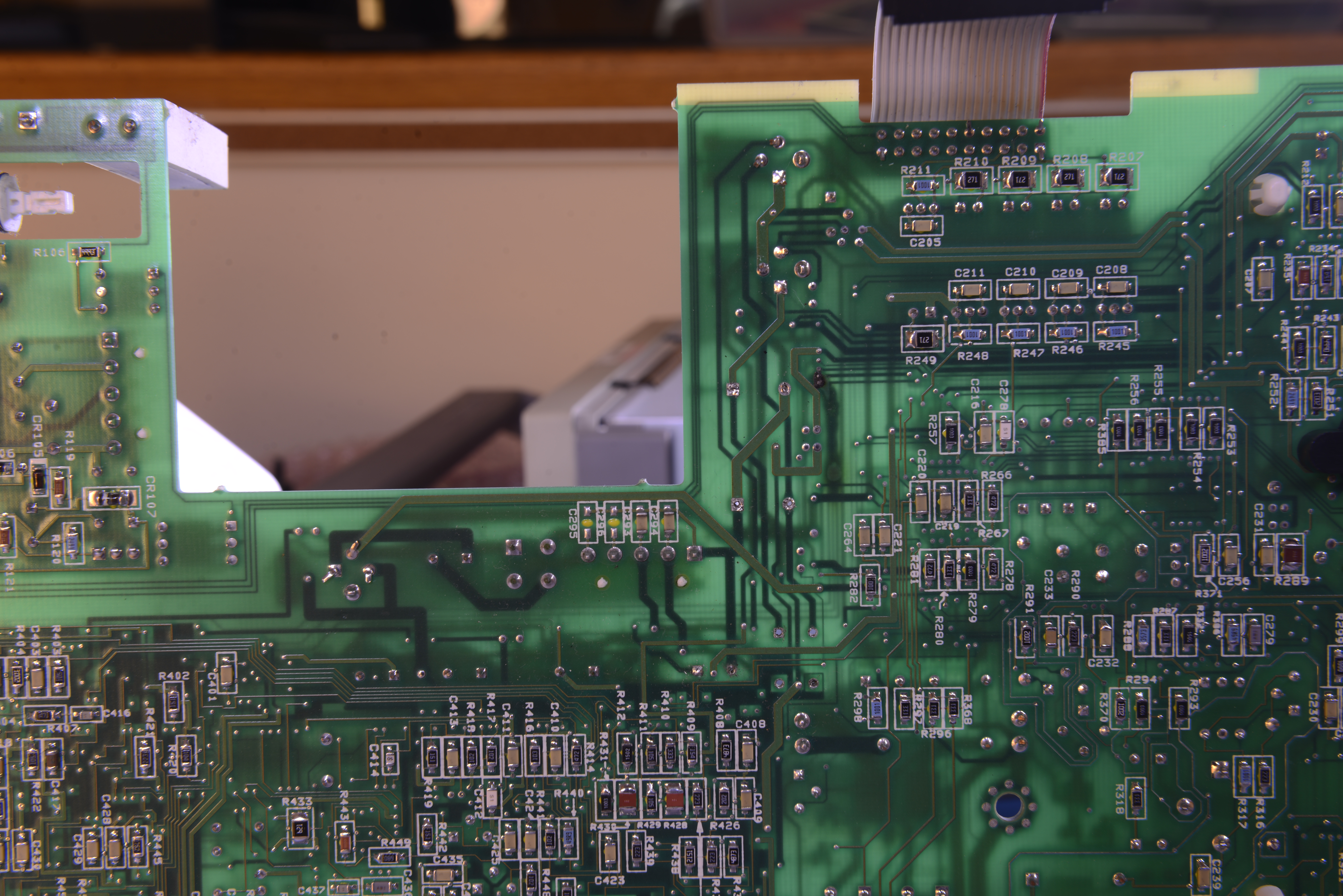
Another update on repair process. I removed all components affected by the spill. They were easy to identify under microscope. This is a full resolution image of the board after the cleanup. For general areas I used canned air with zero oils in it (MG Chemicals super duster 134). Areas with the spill damage were cleaned multiple times with 99% IPA. IPA was not able to remove all the board discoloration. Some corroded pads were scratched a bit with solder wick and re tinned.
I left some dirt around R319, as I was not comfortable desoldering these components, esspecialy precision resistance network. I might try to clean around them with IPA later.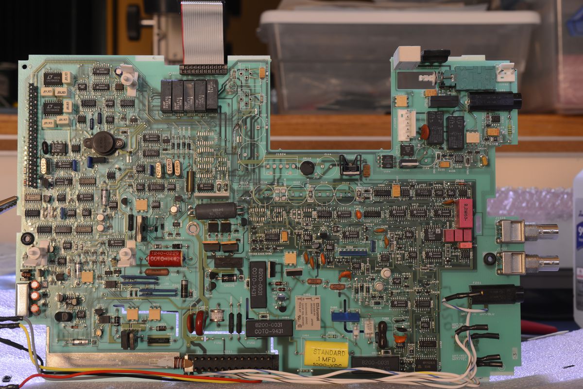
Remarkably only 3 traces were compromised by the burn. Additionally several traces around C116 were eaten away completely.
I took several pictures of copper and component side of analog board. I used light painting technique described by TiN and lit the board from behind to see internal traces. Two images below had been aligned, and flipped in Photoshop to closely correspond to one another. This way you can see traces, including most internal traces, and switch from copper to component side without loosing what you are tracing, but just hiding/un hiding layers. Maybe these will be useful for someone.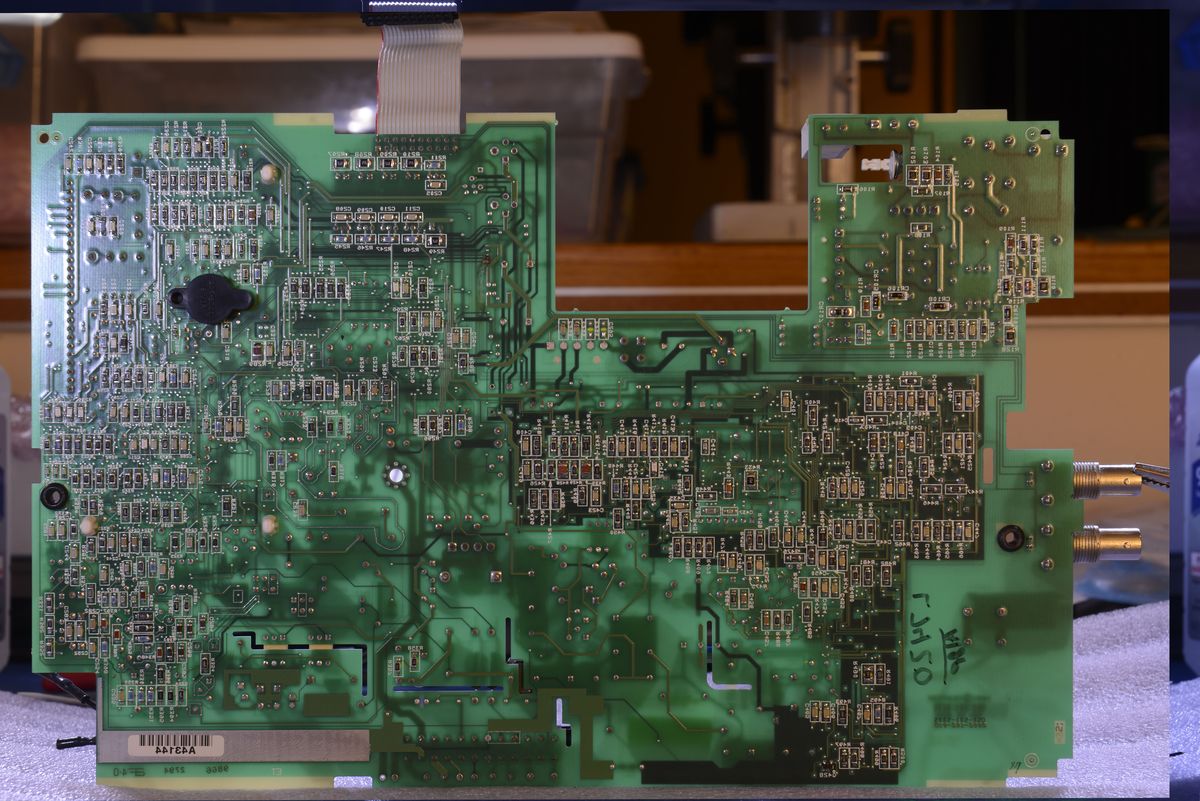

Finally on following two images I colored traces important for my repair. Red is the Component layer, blue and yellow and following internal layers and yellow is the copper layer.
I already started repairs and faced few challenges. My original plan was to solder copper transformer wires to micro vias to fix broken connections. All of my attempts to solder to micro via failed. I even tried to excavate the via a bit by removing a bit of PCB material around it under microscope. So far around capacitor C116 I had to reconnect vias to traces missing .3mm to 1mm of copper. The only way I was able to reconnect them was by forming a "solder bridge" between them. Testing showed them electronically connected and mechanically sound. Any attempt to use copper wire for that failed. While solder bridge solution is far from ideal I would like to hear some opinions.
Any advice on how to solder to micro vias? If I cannot solder to micro vias, 3 traces that were broken will have to be repaired by wires stretching half the way though entire board. Thanks.
-
First things first; great work! The effort you have put in really shows.
As far as getting the transformer wire to bond; what are you using for flux? Are you able to tin the wire first? It seems odd that it is refusing to bond. -
Is the solder not sticking to the via or the wire? The enamel on the wire can be a pain.
And I agree with WastelandTek - great work so far, I really appreciate the post detail. I have no doubt someone else will be helped by it in the future. -
I scraped and tinned the transformer wire first. I used Kester 951 low solids flux pen.
I used same flux on the via.
Via might be corroded with electrolyte or maybe it is just too small and surrounded by solder mask that repels solder. Maybe the gauge of the wire is too big for the via? I just know that I had been trying for a while without good results. -
You might try some no-joke RA flux, I use MG chems 835, pretty aggressive stuff.
PM me your zip, if you're local I have a litre of it...lol