Author Topic: PCB design software with components autoplacers.  (Read 43636 times)

0 Members and 17 Guests are viewing this topic.

Offline tycz

  • Regular Contributor
  • *
  • Posts: 126
Re: PCB design software with components autoplacers.
« Reply #25 on: July 29, 2019, 11:24:04 am »
What a coincidence. I found PCBCAD51 on a list of electronics CAD software two about two weeks ago. I hadn't heard of it before, but the website looked active and the price was cheap so I just went ahead and bought it out of curiosity. I could tell right away that this is really old software. I was thinking late 80s or very early 90s. I used another package of similar vintage for several years and the feel is very similar.

I've only really played with the schematic entry part so far. It's functional, I suppose, but is lacking in modern convenience like copy/paste, undo, mouse panning which is taken for granted these days. I found a few bugs without trying too hard so I'd say it's no less buggy than any other CAD package.

For example,
** If you delete a component, the end of each line that was connected to one of its pins is reset to co-ordinate 0,0.
** Changing the reference angle has no effect.
** The launcher menu program crashes half the time when I close the schematic editor, though I can't figure out how to repeat this consistently. Maybe time related...
** When I click on PCB to Gerber Translator and select the included example layout (single.pcb) the program just complains about a missing file and that there were errors found. It would be great if the example was error free.

Unfortunately there doesn't appear to be any settings to fiddle with at all. No way to change those damn colours that I can see. As side note, I'm pleased to hear that other posters agree the colours are bad (at least I think that's what 'ugly' means in this context). This isn't unique to this program at all - more than half of the electronics CAD software packages I've tried has absolutely eye destroying default colours. Like Altium Designer which (used to?) come default set to 100% blue, 100% red and 100% yellow for bottom, top, and silk layers - all on a black background. It makes me feel uneasy looking at a layout in these colours for more than a couple of minutes at a time. I initially thought that it was just some kind of joke, maybe even a competition between the coders of different packages to see how garish they could make it without the marketing dept insisting it be changed. But since then I've seen a fair amount screenshots, even from people on this forum, showing some work in progress or another with those extremely ugly colours the software defaults to. I'll just say I'm amazed at what some people can tolerate.

Anyway, back on topic. The most annoying problem I can see with PCBCAD51 is screen updates are very slow. It's perfectly fine when you add the first few components on a schematic, but if I open the included example schematic, which has about 80 components, the screen redraw takes about 800ms when zoomed out a bit. Maybe there's a compatibility layer on the graphics that translates the old DOS graphics routines to Windows API. I don't know why it would be so slow otherwise. It's hard to put up with if you are used to panning and zooming around a schematic effortlessly like a modern schematic editor with graphics acceleration can.

I also somehow doubt you've sold anywhere close to 3000 copies of this at full price.

What reason do you have to doubt this? Full price is 5 GBP. I bought it just to play around with, but 15 years ago I would have bought it to use in earnest, and would have paid more than the current asking price. Cheap CAD software that produced Gerbers was not a common thing back then.
 
The following users thanked this post: Mechatrommer, edavid, ebastler, Ysjoelfir

Offline Mechatrommer

  • Super Contributor
  • ***
  • Posts: 11725
  • Country: my
  • reassessing directives...
Re: PCB design software with components autoplacers.
« Reply #26 on: July 29, 2019, 12:23:13 pm »
I think it would be nice if Dave (or Dave2) could do a quick review on this package.
already done 5 years ago...
https://www.eevblog.com/forum/buysellwanted/pcb-design-software-for-sale/msg452313/#msg452313

I hadn't heard of it before, but the website looked active and the price was cheap so I just went ahead and bought it out of curiosity. I could tell right away that this is really old software.
so you are among the 3000 who donated. thanks for making the review and letting us know... that one post thanked ;)

It's functional, I suppose, but is lacking in modern convenience like copy/paste, undo, mouse panning which is taken for granted these days.
so someone may call it features ;D

The most annoying problem I can see with PCBCAD51 is screen updates are very slow. It's perfectly fine when you add the first few components on a schematic, but if I open the included example schematic, which has about 80 components, the screen redraw takes about 800ms when zoomed out a bit. Maybe there's a compatibility layer on the graphics that translates the old DOS graphics routines to Windows API. I don't know why it would be so slow otherwise. It's hard to put up with if you are used to panning and zooming around a schematic effortlessly like a modern schematic editor with graphics acceleration can.
thats why i hinted a major upgrade, to the Win7/10 appearance like, that thing looks like emulated from the past age. so you confirmed it.
« Last Edit: July 29, 2019, 12:27:18 pm by Mechatrommer »
 

Offline free_electron

  • Super Contributor
  • ***
  • Posts: 9053
  • Country: us
    • SiliconValleyGarage
Re: PCB design software with components autoplacers.
« Reply #27 on: July 29, 2019, 02:28:00 pm »
-first go wash my eyes .. i just saw that screenshot of the routed board ... -

i downloaded and played with it for 30 minutes. it feels at the level of Smartwork ... and orcad for dos ... sdt386

1 schematic symbol editor
- symbols are horrible
- no linewidths
- no group selection and move operations. one thing at a time
- no keyboard shortcuts. everything is click

2 footprint editor
- no bulk operations ( select 5 pads and change all of them at the same time )
- no group operations ( select a bunch of stuff and move it )
- no display of locations , no entry of coordinates or coordinate equations ( like add .0.2mm to x of this object )
- pad width and length is from pulldown menus. why not allow entry of numbers ?
- why have both pin and pad in pcb editor. what is function of 'pin' ?

3 schematic editor ( loaded sample schematic.)
- need to go wash eyes again- horrible schematic

other things i could not find : zoom / drag using mouse.
There is a block move but it is very archaic. you need to invoke a command select the block and then you can only move it by clicking a destination point., the block does not follow the mouse in realtime.
middle button is 'center here'.
scrollwheel is zoom in / out ( fixed step)
drawing a line : no panning when hitting edge of viewport
'zoom all' is very sluggish. takes 2 seconds to redraw screen.

does this thing support multiple sheets ? hierarchical schematics ?

my main issue with this tool is that you alwasy need to invoke a command first before you can do anything.
i would expect , in 2019,
- i can just double click on an object (symbol , footprint , track ,pad whatever )  to edit it.
- select things in group using shift-click of left-mouse-drag operations.
- use ctrl-c ctrl-v ctrl-x for cut copy paste
- scroll freely around a viewport with autopan and zoom.

4 pcb editor
- only one global clearance rule
- again no direct editing of objects. very frustrating
- sample layout is horrible (from a layout perspective)

5 3d viewer
see screenshot (and filename)

even simple text editors like notepad and simple drawing programs like paint can do that ...

This really feels like smartwork and orcad under dos.
sorry. not for me.
« Last Edit: July 29, 2019, 02:37:29 pm by free_electron »
Professional Electron Wrangler.
Any comments, or points of view expressed, are my own and not endorsed , induced or compensated by my employer(s).
 
The following users thanked this post: TiN, thm_w, Zucca, Ysjoelfir

Offline nigelwright7557Topic starter

  • Frequent Contributor
  • **
  • Posts: 725
  • Country: gb
    • PCBCAD software
Re: PCB design software with components autoplacers.
« Reply #28 on: July 29, 2019, 03:47:06 pm »
i believe you mixed up with that hand sketched dso pcb thread..

The same PIC32, the same AD9200.

Two different pcb's !
The first one was a quick and dirty prototype.
The second is much tidier.
 

Offline free_electron

  • Super Contributor
  • ***
  • Posts: 9053
  • Country: us
    • SiliconValleyGarage
Re: PCB design software with components autoplacers.
« Reply #29 on: July 29, 2019, 03:48:24 pm »
I'd be happy with software optimized for _manual_ routing.
This.

While computers may be fast at trying millions of combinations , they have no intelligence. And that is the problem with routers.
The human has to intelligently craft a bunch of rules that the machine will then slavishly follow. when it fails to find a solution we go 'autorouters suck'.
No. They dont. it is just a connectivity solving algorithm. you as a human did not feed it proper information , or made such a swiss-chees out of your preroutes the damn thing locks up.
I have to see the first autortoure that goes : hey stupid, if you shidft this stuff over here , move that bunch of tracks to that layer and change the polygon plane like that i can route this.
no. They simply go 'no solution found'. Have you really tried finding one ? or are you just stringing copper from a to b ?

That being said: a word of advice for the maker of this tool

- ditch the 3d efforts. unless you can import/export 3d models (step, idf) to mechanical domain it is just eye candy.
- change the user interface
- if i click on an object ( line,pad part,footprint, whatever) i should be able to manipulate it.
       - hold button-drag = move
       - shift click add to group selection. or remove if already in group
       - ctrl-c ctrl-v  ctrl-x copy paste cut
       - double click : edit properties ( on designator : edits text , on track edit width / layer ) , pad/via : size / shape / hole
- when in operation and hitting window border : pan.
- mouse scrollwheel: zoom
- absolute movements : be able to say move this object ( or group of objects ) 1mm to left and 2.14 mm up by typing in the equation or absolute numbers. all you need is + and -
- free rotation of parts
- in pcb editor : snap to object center ( center of pad , center of via ) when placing final route stub.
- allow more than one clearance rule in pcb
- allow editing of soldermask. it is sometimes necessary to edit this

Then you will have a good base package that is easy to use

oh , and make a library of proper symbols. your resistors are really butt-ugly .
Professional Electron Wrangler.
Any comments, or points of view expressed, are my own and not endorsed , induced or compensated by my employer(s).
 

Offline nigelwright7557Topic starter

  • Frequent Contributor
  • **
  • Posts: 725
  • Country: gb
    • PCBCAD software
Re: PCB design software with components autoplacers.
« Reply #30 on: July 29, 2019, 03:56:38 pm »
I'd be happy with software optimized for _manual_ routing.
This.

While computers may be fast at trying millions of combinations , they have no intelligence. And that is the problem with routers.
The human has to intelligently craft a bunch of rules that the machine will then slavishly follow. when it fails to find a solution we go 'autorouters suck'.
No. They dont. it is just a connectivity solving algorithm. you as a human did not feed it proper information , or made such a swiss-chees out of your preroutes the damn thing locks up.
I have to see the first autortoure that goes : hey stupid, if you shidft this stuff over here , move that bunch of tracks to that layer and change the polygon plane like that i can route this.
no. They simply go 'no solution found'. Have you really tried finding one ? or are you just stringing copper from a to b ?

That being said: a word of advice for the maker of this tool

- ditch the 3d efforts. unless you can import/export 3d models (step, idf) to mechanical domain it is just eye candy.
- change the user interface
- if i click on an object ( line,pad part,footprint, whatever) i should be able to manipulate it.
       - hold button-drag = move
       - shift click add to group selection. or remove if already in group
       - ctrl-c ctrl-v  ctrl-x copy paste cut
       - double click : edit properties ( on designator : edits text , on track edit width / layer ) , pad/via : size / shape / hole
- when in operation and hitting window border : pan.
- mouse scrollwheel: zoom
- absolute movements : be able to say move this object ( or group of objects ) 1mm to left and 2.14 mm up by typing in the equation or absolute numbers. all you need is + and -
- free rotation of parts
- in pcb editor : snap to object center ( center of pad , center of via ) when placing final route stub.
- allow more than one clearance rule in pcb
- allow editing of soldermask. it is sometimes necessary to edit this

Then you will have a good base package that is easy to use

oh , and make a library of proper symbols. your resistors are really butt-ugly .

Pretty much every point you have made is nonsense !
Are you sure it was my software you tested ?
It all smacks of not reading the manual.

You need to use "blockmode" to work on groups of components.
Press F9, left click on top left hand side of block, left click on bottom right hand side of block.

The component wizards are amazing, a few clicks and you have a component.
Lines, pads, text etc can all be manipulated with sizes etc.
 

Online nctnico

  • Super Contributor
  • ***
  • Posts: 30196
  • Country: nl
    • NCT Developments
Re: PCB design software with components autoplacers.
« Reply #31 on: July 29, 2019, 04:31:39 pm »
from youtube, i still can see one most noticeable bug... it looks a little bit oldish, i hope you can fix that to be more modern than GUI like Altium at least, or Cadence Allegro better, and then differential and length match routing supported? any example?
I wouldn't call the GUI on Orcad Allegro modern. It is straight from the Unix mainframe/ X-terminal era. But once you get the hang of it, it is quite productive.
There are small lies, big lies and then there is what is on the screen of your oscilloscope.
 

Offline Mechatrommer

  • Super Contributor
  • ***
  • Posts: 11725
  • Country: my
  • reassessing directives...
Re: PCB design software with components autoplacers.
« Reply #32 on: July 29, 2019, 05:20:39 pm »
there comes "the community" i hoped they will come and follow my soft tone but... the truth will always prevails..  ;D

from youtube, i still can see one most noticeable bug... it looks a little bit oldish, i hope you can fix that to be more modern than GUI like Altium at least, or Cadence Allegro better, and then differential and length match routing supported? any example?
I wouldn't call the GUI on Orcad Allegro modern. It is straight from the Unix mainframe/ X-terminal era. But once you get the hang of it, it is quite productive.
yeah i could be mistaken. i saw some members posted their pcb rendering with semi transparent colorful layers on black background. i know its not allegro (nor altium) by looking at the website, but i just talk out of my arse hopefully the OP get the idea. otoh, i was talking about the earlier more polished eda, is this... https://www.dexpcb.com/ not meaning to hijack, just for learning and lesson or food for thought, even that, its not functionally entertaining either.
 
The following users thanked this post: Ysjoelfir

Offline james_s

  • Super Contributor
  • ***
  • Posts: 21608
  • Country: us
Re: PCB design software with components autoplacers.
« Reply #33 on: July 29, 2019, 05:23:16 pm »
Auto-routing is useless, auto component placement is even worse. I mean maybe if you're making PCBs for 1970s-80s childrens toys it's fine, but not for anything modern.

I'll stick to KiCAD, it's powerful, reasonably modern, easy enough to use, I have few complaints about it these days and it costs nothing.
 

Offline Mechatrommer

  • Super Contributor
  • ***
  • Posts: 11725
  • Country: my
  • reassessing directives...
Re: PCB design software with components autoplacers.
« Reply #34 on: July 29, 2019, 05:54:44 pm »
yeah but routing buses, match length serpentines, differential and impedance control traces are much more important nowadays which eda newcomers often overlook, imho.

Offline Bud

  • Super Contributor
  • ***
  • Posts: 7928
  • Country: ca
Re: PCB design software with components autoplacers.
« Reply #35 on: July 29, 2019, 06:21:17 pm »
Quote
Touch screen compatible

 :-DD
Facebook-free life and Rigol-free shack.
 

Offline TiN

  • Super Contributor
  • ***
  • Posts: 4543
  • Country: ua
    • xDevs.com
Re: PCB design software with components autoplacers.
« Reply #36 on: July 29, 2019, 07:07:50 pm »
Ugh, my eyes... why.... why would electronics engineering person pay for this?
Because they don't know there are free PCB EDA tools, no other reason.  :palm:
YouTube | Metrology IRC Chat room | Let's share T&M documentation? Upload! No upload limits for firmwares, photos, files.
 
The following users thanked this post: Ysjoelfir

Online nali

  • Frequent Contributor
  • **
  • Posts: 891
  • Country: gb
Re: PCB design software with components autoplacers.
« Reply #37 on: July 29, 2019, 07:56:22 pm »
I'm searching the back of my memory to recall what that delightful black-on-cyan menu bar reminds me of. Something 1990s for sure, maybe the early Macs or Amigas perhaps?
 

Offline thm_w

  • Super Contributor
  • ***
  • Posts: 9804
  • Country: ca
  • Non-expert
Re: PCB design software with components autoplacers.
« Reply #38 on: July 29, 2019, 09:00:48 pm »
-first go wash my eyes .. i just saw that screenshot of the routed board ... -
...
This really feels like smartwork and orcad under dos.
sorry. not for me.

I'm seriously impressed that you gave this a fair try out after seeing the screenshots.
Profile -> Modify profile -> Look and Layout ->  Don't show users' signatures
 

Offline nigelwright7557Topic starter

  • Frequent Contributor
  • **
  • Posts: 725
  • Country: gb
    • PCBCAD software
Re: PCB design software with components autoplacers.
« Reply #39 on: July 30, 2019, 12:05:25 am »
I look at that screen shot and it's hard on my eyes. The blue or green(not sure) keeps changing colors on me. Parts of your tracks are hidden some don't seem to connect with vias where they should... It's just too ugly to ever bother blindly switching from what I know. I'm not sure if I'm seeing software issues or designer issues. Best of luck but I'll never touch it.
Its a low res bitmap screen dump !
Its only a bitmap file so you can texpect much.


Online nctnico

  • Super Contributor
  • ***
  • Posts: 30196
  • Country: nl
    • NCT Developments
Re: PCB design software with components autoplacers.
« Reply #40 on: July 30, 2019, 12:08:13 am »
-first go wash my eyes .. i just saw that screenshot of the routed board ... -
...
This really feels like smartwork and orcad under dos.
sorry. not for me.

I'm seriously impressed that you gave this a fair try out after seeing the screenshots.
Still the conclusion is 'this doesn't work like Altium'. Then again: does the world really need another schematics + PCB layout package? There are more PCB packages than flavours of ice cream.
There are small lies, big lies and then there is what is on the screen of your oscilloscope.
 

Offline legacy

  • Super Contributor
  • ***
  • !
  • Posts: 4415
  • Country: ch
Re: PCB design software with components autoplacers.
« Reply #41 on: July 30, 2019, 01:08:31 am »
There are more PCB packages than flavours of ice cream.

A few choices:
  • EagleCAD (Commercial)
  • KiCad (OpenSource)
  • Altium (Commercial)
  • OrCad (Commercial)
  • DipTrace (Commercial)
  • gEDA (OpenSource)
  • pcb-rnd (OpenSource, I am personally supporting it on Gentoo/HPPA)
 

Offline free_electron

  • Super Contributor
  • ***
  • Posts: 9053
  • Country: us
    • SiliconValleyGarage
Re: PCB design software with components autoplacers.
« Reply #42 on: July 30, 2019, 01:08:37 am »


Pretty much every point you have made is nonsense !
I handle 5 to 6 board a week. up to 16 layers, some with 5000 pin bga's. tell me again my points are nonsense.

Quote
Are you sure it was my software you tested ?
yup. free version

Quote
It all smacks of not reading the manual.
what manual ? and who needs a manual ? ctrl-c ctrl-v ctrl-x , clicking and drag are all standard operations in any kind of software , whether notepad, word, autocad ,or a pcb editor.
Software MUST be intuitive to use. It is assumed if i click on an object i can do something with it (it should at least select or highlight it) . To select a group of object : hold left mouse button and drag, anything fully enclosed is now selected. There is no need to invoke F9 for 'block mode'.

Quote
You need to use "blockmode" to work on groups of components.
Press F9, left click on top left hand side of block, left click on bottom right hand side of block.
there's my point. f9 to invoke, click top left , click bottom right. that is counterintuitive to any other windows program. also click top left click top right : i'd like to see a bounding box when i am in mid selection.(pcb does do that, schematic does't...)
another point L: now that i have this lump of stuff selected : hoe do i add something to the already selected group or remove something from the selected group ?

Quote
The component wizards are amazing, a few clicks and you have a component.
that doesn't conform to any standards (IPC). SIL DIL and quad. How about  QFP ? SON ? DFN ? QFN ? BGA with thermal pads ? in the wizrd i see no option to specify top layer only pads or set the hole size to zero so i assume SMT is not supported ?

Quote
Lines, pads, text etc can all be manipulated with sizes etc.
yes they can .
but : bulk operations ? select a number of traces and adjust all of them to 10 mils in one shot ?
select a trace end to end ? (all segments on all layers
select a trace between two pads ? ( all segments on current layer)
zooming is counter intuitive. you need to first click to make the clicked point the center of the screen, then scrollwheel to zoom. zooming should happen around the current cursor location. there is also no free panning. (hold some mouse button down and the viewport follows you )

Other trouble i ran into :
- selecting traces to edit
  hit F1 , now click on a segment of a track. The cursor jumps to the closest bending point ,irrespective if it is on the track clicked or not.
I can't figure out how to add or remove bending points. the help doesn't show.


on the attached picture ( from the single.pcb file)
please explain how to :

1) select the light blue section of track. only that section , the portion going from pin 40 upward is not to be selected. and then change the selected section to 5 mils.

2) select the dark blue traces in one operation. decrease their size with 2 mils. ( from whatever they are) Note that the vertical portions of these tracks are different from the horizontal portions. so we are not going to set absolute widths , but relative from what they already are.

3) grab the segment in the yellow circle and push it towards bottom left. if it comes within minimum allowed distance from the gray trace it should stop moving. ( or ideally start pushing the grey trace also. but lets first stop at design rule violation)

4) modify the right hand vcc trace to add the magenta section.

Because i can't figure out how to do these simple tasks.
Maybe i am stupid, but i do know how to do these in smartwork, tango, Orcad, Autotrax, Protel , altium , Tanner EDA , Cadence, Pcad, Pads , Hiwire, and a few other pcb layout programs. I can't figure it out in PCBCAD51 ..

The above things are basic operations that any pcb cad program needs to be able to do in a fast way ( fast meaning : least amount of operations on keyboard / mouse.)

« Last Edit: July 30, 2019, 01:13:20 am by free_electron »
Professional Electron Wrangler.
Any comments, or points of view expressed, are my own and not endorsed , induced or compensated by my employer(s).
 
The following users thanked this post: TiN, exe, Ysjoelfir

Offline digsys

  • Supporter
  • ****
  • Posts: 2239
  • Country: au
    • DIGSYS
Re: PCB design software with components autoplacers.
« Reply #43 on: July 30, 2019, 01:46:56 am »
Quote from: free_electron
... it feels at the level of Smartwork ... 
OIII don't knock Smartwork !! I used it for many years and literally did 100s pcbs on it - plus it was easy to re-engineer and get into the data files.
I created graphics files / viewers, assembly overlay programs etc I really only switched back then, when they stopped advancing it, and my new favourite Proteus came out !
Hello <tap> <tap> .. is this thing on?
 

Offline Mechatrommer

  • Super Contributor
  • ***
  • Posts: 11725
  • Country: my
  • reassessing directives...
Re: PCB design software with components autoplacers.
« Reply #44 on: July 30, 2019, 02:30:13 am »
Still the conclusion is 'this doesn't work like Altium'. Then again: does the world really need another schematics + PCB layout package?
yes we do, something that works better than Altium yet affordable like DipTrace. maybe an Utopia dream, but until someone with "open source software" or "great" mind take the challenge. no we dont need another that works worse than KiCAD or Eagle.

Quote
You need to use "blockmode" to work on groups of components.
Press F9, left click on top left hand side of block, left click on bottom right hand side of block.
there's my point. f9 to invoke, click top left , click bottom right. that is counterintuitive to any other windows program.
thats a feature, along with the other features you mentioned. what do you know? the OP designed 300 pcbs with those features >:D
 
The following users thanked this post: Ysjoelfir

Offline nigelwright7557Topic starter

  • Frequent Contributor
  • **
  • Posts: 725
  • Country: gb
    • PCBCAD software
Re: PCB design software with components autoplacers.
« Reply #45 on: July 30, 2019, 03:26:23 am »
I have read all your criticisms and I have to say once again that you clearly haven't bothered reading the manual.
I have no problem editing anything.
If I did I wouldn't be able to design any pcb's never mind the 300+ I have already done and the many thousands my customers have designed.

Some people get taken in by massive screens of toolbars etc.
I chose not to do that and leave the screen for laying out pcb's etc.
Not every one has a 36 inch pc monitor !
Some of the other software I have seen barely leaves any room for a schematic or pcb.

If you lived a bit closer I would have come round and showed you how to use it because you are clearly clueless !
Its simply one "cant use it so will diss it" lie after another.
I can only guess you are a competitor and need to drag everyone elses software down to make yours look good.

You haven't yet mentioned the extremely low price. This software has functions I haven't even seen on software costing many hundreds of pounds.
Anything mine has missing is because I never found a need for it or no one has ever asked for it.
 

Offline free_electron

  • Super Contributor
  • ***
  • Posts: 9053
  • Country: us
    • SiliconValleyGarage
Re: PCB design software with components autoplacers.
« Reply #46 on: July 30, 2019, 03:59:14 am »
Quote from: free_electron
... it feels at the level of Smartwork ... 
OIII don't knock Smartwork !! I used it for many years and literally did 100s pcbs on it - plus it was easy to re-engineer and get into the data files.
I created graphics files / viewers, assembly overlay programs etc I really only switched back then, when they stopped advancing it, and my new favourite Proteus came out !
i started with smartwork. made probably 50 boards with it during my school years when all we had was 8088 based pc's.... it worked fine . i still miss its ability to shave pads to run a trace ...
i really liked that tool. dip e 28 600. draw a dip package eastward 28 pins 600 mil pitch f1 place pad f2 remove pad f3 place wire f4 remove wire f5 thick wire.

but then you find better tools... and you move on.

Professional Electron Wrangler.
Any comments, or points of view expressed, are my own and not endorsed , induced or compensated by my employer(s).
 

Offline free_electron

  • Super Contributor
  • ***
  • Posts: 9053
  • Country: us
    • SiliconValleyGarage
Re: PCB design software with components autoplacers.
« Reply #47 on: July 30, 2019, 04:41:28 am »
I have read all your criticisms and I have to say once again that you clearly haven't bothered reading the manual.

so where is this manual ?
all i can find is the help in the program itself and that is of no help.
And no i am not a competitor. If you'd care to google me you'd know better.
I have been making PCB's since i was 8 years old. i etched my first board using left over material fro a local TV manufacturer , a sharpie pen and a bottle of FeCl. When i was 15 years (1985) i got a hold of a 8088 pc ( some clone made in Egypt .. forgot the brand ) and a copy of Winteks Smartwork (https://smores.tistory.com/810) and made maybe 50 boards with that during my school years. We also had access to OrCad under dos. Later on i started using easytrax , autottrax and all versions of Protel / Altium. Professionally i have used many PCB tools ( PCAD, Pads, Tango , Vanguard, Cadence, OrCad and a few very esoteric ones running on Sun or Apollo workstations to design hybrid modules ). I don't work for any Cad software company. I'm a user.

I have no personal interest in any CAD tool. my interest is purely out of curiosity.
i would like there to be a simple to use schematic/pcb tool and so far i have not found anything. I am not interested for my self as i have my own paid licences of the big tools. It's more of a 'community thing'.
The whole open source stuff does not appeal. The tools are not usable in an easy way. it is not a coherent package , everything is bolted together from various bits and pieces and in a constant state of flux.

My feedback is based on how easy i find it to pick up a new tool. but, my patience is very thin. I expect tools to have a basic 'common' feel with other programs. ( like screen navigation, object selection , copy paste etc. )
Those are basic operations that work identical irrespective of what the software does or what platform it runs on.
zooming and panning does not work like 'normal' programs. For starters : why don't you have simple scrollbars bottom and right like all programs do ?
Most software allows free panning by holding right mouse button and dragging.
you have a bunch of shift-clcik , ctrl-click but what i want is hold a button , move mouse and the viewport scrolls realtime where i point. All graphical software works that way. Paint, Photoshop , Autocad, Solidworks , doesn;t matter what.
Having a UI that is completely different in basic manipulations is an obstacle for people.

Please do explain how i can do something simple like this : note : i looked in the online help and in the 'manual button' in the software itself. i searched for copy and paste. there is not a single word about that.
so do explain : how do i select some components , net names and wires , make a copy of that block and paste it in the schematic.
The usual menu items i'd expect like copy and paste don't exist. ctrl-c ctrl-v doesn't do anything. Right click doesn't show anything obvious on the menu either. Searching for 'copy' or 'paste' in the help file also yields nothing.
So please do tell : how do i copy and paste a section ?

And no , 'repeat' is NOT an obvious command, besides it doesn't work as it garbles all the netnames and makes spaghetti out of the pasted block.

Second point : look at the picture : how do i make a selection like in the blue polygon. just being able to make rectangular selections is very restrictive.
In most software (even if it is not pcb software) you can create subselections using ctrl-click or shift-click. they add or subtract elements to the already selected items.
How do i do this basic operation ?

or is there another problem ? i am using PCBCAD51 the freeware version.

-edit- oh, and can we please an 'undo'  ? if you forget to get out of that block mode and click somewhere you destroy half of your work ... (see picture 2). i searched the help for 'undo'. nothing found. it's 2019 ... undo is so 1970's ...

Even the Calma GDS layout system running on a Nova computer had a 16 level deep undi/redo stack in 1975
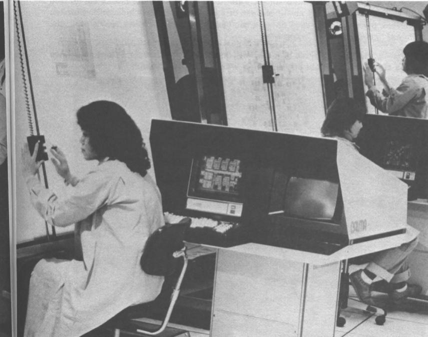
« Last Edit: July 30, 2019, 04:54:40 am by free_electron »
Professional Electron Wrangler.
Any comments, or points of view expressed, are my own and not endorsed , induced or compensated by my employer(s).
 
The following users thanked this post: Ysjoelfir

Offline nigelwright7557Topic starter

  • Frequent Contributor
  • **
  • Posts: 725
  • Country: gb
    • PCBCAD software
Re: PCB design software with components autoplacers.
« Reply #48 on: July 30, 2019, 05:53:11 am »
Copy and paste is done by selecting the area you want to copy and paste. I think its right at the end of the help manual.
You have to set up blockmode otherwise I don't know what area wants copying.
Press F9 then left click on top left hand side of block.
Move mouse button to bottom right hand side (you will see a moving rectangle as you move the mouse)
Left click mouse button on bottom right hand side and rectangle will become set around the area.
Now right click mouse button and a context menu will appear with lots of options like print, repeat, rotate,  etc.

The manual is found by clicking on "help" on top menu bar.

I had completely forgotten about the schematic moving all disconnected lines to a deleted component to bottom left hand side corner.
I always delete the tracks first before deleting the component.
However, I can see how some people would be put off by this.
So I spent 10 minutes tonight fixing it.
Not only that but the software now allows laying new components over lines and it automatically connects to them.
It only needs to do this for component repeat, new component and block repeat.

The pcb has the same problem but that is overridden by "forward annotate" which will align connectivity with the schematic which is how the software "should" be used.


Offline Spirit532

  • Frequent Contributor
  • **
  • Posts: 520
  • Country: 00
    • My website
Re: PCB design software with components autoplacers.
« Reply #49 on: July 30, 2019, 06:20:06 am »
Skipping undo, a basic feature back in the early seventies, makes your software worth less than $0. You'd have to pay me to even think of using it.


Share me

Digg  Facebook  SlashDot  Delicious  Technorati  Twitter  Google  Yahoo
Smf


-->