-
HDL compilers love to spit out warnings about all sorts of things so you usually won't get a zero warning zero error compilation like you tend to strive for in most other programming, If nothing else it will spit out a warning that it is not fully licensed.
and it is freaking annoying, because sometimes somewhere in the ten pages of silly warnings something important is hidden -
HDL compilers love to spit out warnings about all sorts of things so you usually won't get a zero warning zero error compilation like you tend to strive for in most other programming, If nothing else it will spit out a warning that it is not fully licensed.
and it is freaking annoying, because sometimes somewhere in the ten pages of silly warnings something important is hidden
Hun, yes, with Altera, I turned off the 32bit integer warning, however, when I compile, I get no other warnings.
I used to when I started, but I once I started coding with individual projects for individual .v modules, and I coded for 0 warnings, (only after around 4 years of using Quartus) no more warnings, even when my main project use all the child .v modules into my authentic design.
It's a hassle, but it locks you down to proper coding and using the tool properly. And now, only important warnings or errors show up in the build log.
-
It seems the warning is due to the literal values '0' and '1'? Any way around that?
By googling quartus warning 10230 I found Intel recommending explicit width specification on constants to suppress the warning.
Yes, found the same page last night - the code doesn't read as clearly now, but by replacing 1's and 0's with 1'b1s and 1'b0s, the warnings have mostly gone away now. Quote
QuoteI have assigned the signals to pins in the Pin Manager, but I'm clearly missing something else important as well?
I consider warnings in a synthesizer as polite FYIs. Unfortunately, that means I have to think when reviewing the warnings to see if they really are a problem, to see if something I really needed got simplified away.
Chalk it up to my inexperience in this field, and my not-insignificant OCD when it comes to compilation errors.
Can we have a look at vga01.v? And your top file? Are you actually driving them? Do you need to drive them? The 13410 will probably not be a real problem of its own, if it resolves once you have provided drivers for that output port, and if you want them "stuck" at 0.
Of course, I attached both files earlier in the thread. I'll probably attach updated copies in this message as well.Another note, it helps readability to use the C conventions for the case of constants (all caps) vs. variables (not all caps).
The dangers of cut 'n' paste code.
Although:
Code: [Select]// generate sync signals (active low for 640x480)Is absolutely correct, however, the >= comparison and < do eat up gates when compiling and your output driving a pin will be a combination unlatched logic equation directly based on your output counter bits. To get a clean output and better F-Max allowing Quartus's Fitter to better route the logic in your FPGA to meet timing constraints, I would:
assign hsync = ~((h_count >= HS_STA) & (h_count < HS_END));
assign vsync = ~((v_count >= VS_STA) & (v_count < VS_END));
A) Make Hsync and Vsync a register.
B) Inside your if (pix_enable), make the logic look like this
if (h_count == HS_STA) begin
hsync <= 1;
end else if (h_count == HS_END) hsync <= 0;
if (V_count == VS_STA) begin
vsync <= 1;
end else if (h_count == VS_END) vsync <= 0;
Okay, I think I follow, although I've had to go off and look at Blocking and Non-Blocking, registers vs wires and all kinds of stuff. Can't remember who said it, but they were right when they said I'd learn a load of stuff just getting a blank screen to display... I haven't even gotten near wiring this up yet! Attached at the bottom are the two updated files with all the changes made.
Can I assume that the non-blocking <= assignment operators are okay in the context in which I'm using them?*Being registers, this now means that those outputs are delayed by 1 pixel clock, but, those outputs will be cleanly timed to the rising edge of your fpga PLL internal clock as those DFF register outputs don't have any logic gates to go through, those DFF register outputs will feed the IO pin directly. (Though, I usually add another DFF stage/pipe to all my DAC and sync outputs allowing the compiler/fitter to bury the logic anywhere deep in the FPGA, the use each pins macrocell flipflops registers to drive the pin itself generating the cleanest possible outputs.)
Sheesh there is so much to learn...
As for your Assign X&Y, again, doing all that realtime arithmetic is not a problem:
Code: [Select]// keep x and y bound within the display area
assign x = (h_count < DA_STA) ? 0 : (h_count - DA_STA); // x is zero if current pixel is before display area
assign y = (v_count >= VA_END) ? (VA_END - 1) : (v_count); // y is VA_END-1 if v_count is outside display area
However, like the HSync and Vsync, personally, I make these outputs a single bit which turns on or off using the simple equality == trick I used to generate the Hsync and Vsync. I rely on my video graphics generator to have an address generator which may increment count every single, every second, or every third/fourth line.
You lost me here. x and y are wires with 10-bit values. I can't make them a single on/off bit - unless you're talking about creating a couple more registers to use as single-bit flags to indicate whether we're in the display area or not?Also, not just that one master image X&Y output enable which is REQUIRED by all DVI transmitters and which may also be used as an image crop mute to protect the video output borders for analog VGA dacs (outside the active video area, the RGB level must be always black), I usually would have something like another 16 programmable of these X&Y on and off output flags which may be used to position sprites or superimposed hardware video windows. Among these 16, which may be positioned after the active video region output, allotting a time slot which may be used to signal memory access cycles to fill your audio DAC buffer, or signal load a new set of X&Y video memory pointers from memory which change the beginning video read address of the next line of video allowing you to dynamically have a new video address and video mode on each new video line. (EG like the Atari 800 display list which allows for a few lines of text mode, then a few with graphics, then more text at a different resolution, or Amiga pulldown screens with a vertically scroll-able window on top of another, each with a different graphics mode pointing to somewhere different in memory.)
Ah okay, I understand. Well, I'm trying to crawl before I walk or run, so I'm not going to add in loads of elements that I won't be using for a while, but that's certainly a consideration down the line.If you still directly want to use you h_count and v_count as reference pixel counters and get rid of the ensuing subtraction math to improve FMAX, I would move your hsync and vsync to the end of your counters so that 0 through 639 and 0 through 479 are passed through without any math while the blank front & back porches with syncs come at then end after pixel 640 and line 480. I personally still prefer the 1 bit enables which can actually tell you ensuing logic when to start and stop reading, or when there is free time to read memory for other purposes. With your current code, your logic will continue reading pixel 0x0 whenever there is no video being outputted.
Sure thing - okay, so I've moved the display area to the start of the v_count and h_count range; hopefully I've got the localparams right for the relevant values, I've added a 'blanking' output to the sync_generator which goes high whenever the generator is in the vertical blanking area. No doubt I'll need to add one for h_count as well to make sure the RGB values are black when in those areas.
EDIT:
Obviously there's errors in the attached files - I'm working through those right now.
-
Just a thought regarding the CPU part itself. Of course you could consider using a Z80 core in the FPGA you're going to use. But if you still want a true CPU IC, you could consider the Z180 series. They are software compatible with the Z80, but contain many improvements and embedded peripherals, and there are 3.3V versions as well. The Z8L180 is readily available for instance (at least at Mouser)... so unless you really want to go for a true, vintage Z80, that would be sometthing to consider.
https://en.wikipedia.org/wiki/Zilog_Z180
-
Just a thought regarding the CPU part itself. Of course you could consider using a Z80 core in the FPGA you're going to use. But if you still want a true CPU IC, you could consider the Z180 series. They are software compatible with the Z80, but contain many improvements and embedded peripherals, and there are 3.3V versions as well. The Z8L180 is readily available for instance (at least at Mouser)... so unless you really want to go for a true, vintage Z80, that would be sometthing to consider.
https://en.wikipedia.org/wiki/Zilog_Z180
I still might create a CPU card with the Z180 on it - I've got a couple of Z180's and Z280's lying around with that purpose in mind, but for the moment I'm using a good old-fashioned DIP Z80 chip (a 10MHz one admittedly, but otherwise quite similar to my first computer).
-
Ok, what the non-blocking statement ( <= ) does and a bit on making optimized fast compact code: What I'm describing here is a little of whats going on inside the compilers mind, and how it wires gates in the FPGA according to the example verilog code. Remember, there is no single core math unit in these FPGAs, whatever you write is literally constructed by wiring masses of gates inside the FPGA. All these wires have lengths, propagation delays, and the gates' inputs have capacitive loads which further slows everything down. This primer gives you an example of coding technique to be aware of to achieve a minimal gate count FPGA core which is fast as possible and lowest power consuming design. (If you wanted a central math processing unit, you literally need to code one into existence and wire it up into your design.)
See attached image: (if you got a color printer, print this one)
There are 3 simplified versions of code in the illustration.
In V1, the 'hsync' is generated just like in the op 'nockieboy' first 'Sync Generator' code.
You have the 10 bit register ''[9:0]'' h_count, which is truly 10 D flipflops. At the 10 data inputs of the 10 D flipflops, all parallel clocked by the (positive edge of 'clk'), the 10 Q outputs h_count is sent through a bunch of gates added to a fixed 1 bit value of '1', with that new 10 bit result fed back into the 10 D inputs of the 10 D flipflops which is the 10 bit register 'h_count'
Now, to make that 'hsync' wire, those 10 Qs of h_count need to be wired to a set of gates which subtract it from the 10 bit parameter number 'HS_STA' to check to see if the result is not negative, while more wiring of the 10 Qs of 'h_count' are fed into another mass of gates to SIMULTANEOUSLY subtract that same 10 bit 'h_count' with the 10 bit parameter value of 'HS_END' to see if the result is negative, and finally, those 2 comparisons checks are ANDed together, inverted generating a final single WIRE result labeled 'hsync'.
To understand what is happening, the compiler and fitter has to wire up the FPGA with all these gates to make to 2 comparisons as well as the +1 for the counter itself. Now, find a TTL data book with a 8bit - 8bit adder/subtract with negative flag. How many gates are there? The FPGA has to do this 2 fold, with 10 bit numbers each. (Ignoring the compiler optimizations for now.) With all that signalling and load, how clean will the 'hsync' wire be if it is driving an IO pin and any other set of logic gates in your design? Remember, things like load and delay of routing all these wires in the FPGA are taken into account even though you as the programmer aren't specifically told by the compiler other than after a design is compiled, X number of MHz is the best your design will achieve without errors.
In V2, this one is identical to V1 except that I changed 'hsync' from a wire into a register. The reason why this is an improvement is because, throughout the FPGA, all of the 'D' flipflops clock inputs have a dedicated hard-wiring making sure that all their outputs are parallel. Example, if your clock is 1 MHz, at the D input of the D flipflop register which is the 'hsync' register, when a clock comes in, the 10 bit 'h_count' with a matched clock will change to it's new value, those 10 bits will go through the mass of gates which are the 2 subtractions and & gate to determine if the number is within 'HS_STA' and 'HS_END', then that result will be presented to the D input of the 'hsync' D flipflop register, however, (and this is the SYNCHRONOUS magic), the Q of the 'hsync' register will not change until the next clock. This means that after all the number comparing, if the result takes 1ns, 5ns ,6ns,10ns, 15.2ns, 33.8ns, or any number less than 1000ns (I said 1MHz clock as an example), with that mess of gates, that D input may even be filled with glitches/noise/invalid states, as long as the correct result is ready by the next rising clock, that Q output as well as all the Qs of all the registers in your design will all snap to their new values at the same time.
So with this V2, if your 'hsync' register drives an IO pin, or if the 'hsync' is used elsewhere in your design, it will be a fast clean signal which is valid within a fraction of the rising positive edge of the 'clk' signal. The 1 negative here is that the 'hsync' result is now delayed by 1 clock, but in this case, it is easy enough to subtract 1 from the 'HS_STA' and 'HS_END' parameters. This change will allow the FPGA compiler to construct a much higher maximum operating frequency for your design, especially if the 'hsync' signal is used elsewhere in your design.
Now in 'V3', the goal here is to make the design operate as fast as possible no mater what the values of 'HS_STA' and 'HS_END'. The change I made was turn the 'hsync' register into an equivilant clocked SR-Flipflop. The code I wrote was if the 'h_count' = 'HS_STA', to turn on the 'S' in the flipflop. Looking above, at the equivilant adder/subtraction and the complex web of gates required for the math, compare all that required to perform an '=' test function which would only be 10 XOR gates whose outputs feed a single 10 input NOR gate. (This is all it takes to create the function: does 'A=B'?) That A=B function would run sub nanosecond in the FPGA compared to a 10bit number A minus 10bit number B function, originally requiring 2 of them in parallel. Just the input load of all those gates in the subtract function slows things down, never mind the delay in each gate as well as the extra length in all the routed wiring. The second half, if 'h_count' = 'HS_END', turns on the R of the SR-Flipflop clearing it to low. The load in wiring of this on the FPGA silicon is a fraction of the above code, except for 1 caveat: If 'h_count' never reaches 'HS_STA', then 'hysnc' will never turn on, or if 'hsync' is on and the 'h_count' never reaches 'HS_END', the 'hsync' will never turn off.
For legibility, the code in the graphic image in plain text:Code: [Select]Many things omitted for simplicity sake but at the top:
module sync_gen ( clk, hsync, hcount );
parameter HS_STA = 10 ; //Turn on hsync signal position
parameter HS_END = 210 ; //Turn off hsync signal position
input clk;
output hsync;
output hcount;
---------------------------------
V1
---------------------------------
reg [9:0] h_count;
wire hsync;
assign hsync = ~((h_count >= HS_STA) & (h_count < HS_END));
always @(posedge clk) begin
h_count <= h_count + 1; // Without a reset limit, the h_count will run 0 to 1023.
end
---------------------------------
V2
---------------------------------
reg [9:0] h_count;
reg hsync;
always @(posedge clk) begin
h_count <= h_count + 1;
hsync <= ~((h_count >= HS_STA) & (h_count < HS_END));
end
---------------------------------
V3
---------------------------------
reg [9:0] h_count;
reg hsync;
always @(posedge clk) begin
h_count <= h_count + 1;
if (h_count == HS_STA) begin
hsync <= 1;
end else if (h_count == HS_END) begin
hsync <= 0;
end
end
---------------------------------
endmodule
-
Ok, what the blocking statement ( <= ) does and a bit on making optimized fast compact code: What I'm describing here is a little of whats going on inside the compilers mind, and how it wires gates in the FPGA according to the example verilog code. Remember, there is no single core math unit in these FPGAs, whatever you write is literally constructed by wiring masses of gates inside the FPGA. All these wires have lengths, propagation delays, and the gates' inputs have capacitive loads which further slows everything down. This primer gives you an example of coding technique to be aware of to achieve a minimal gate count FPGA core which is fast as possible and lowest power consuming design...
Wow - thanks BrianHG!
If I'm doing it right, the v3 counter implementation in Quartus II is quoting an Fmax of 217.2 MHz for clk (that's including the vga01.v top level as well).
It still amazes me when I have to keep reminding myself that the code I'm writing has a physical consequence in the FPGA - so what appears to me to be the easiest way of programmatically achieving a task may actually be quite costly in terms of hardware.
I haven't had a lot of time to look at my code or the hardware this weekend as I've been working, but I've got the FPGA connected to one of my LCD monitors via VGA with just GND, HSYNC and VSYNC connected at the moment. I've messed with the clock timing and tried connecting it at 25 MHz, which showed a corresponding incorrect frequency input on the LCD monitor, but if I get anywhere near the right frequency for VSYNC and HSYNC, the screen is just blank for a few seconds then goes into power saving, so I'm guessing the LCD is (correctly) not detecting any RGB input and is going to sleep as a result. I was hoping to be able to get the menu up and see what screen resolution was reported, but it seems I need to get RGB signals up and running first.
-
Sometimes its better to write HDL code from the perspective of circuit design rather than from a perspective of programming.
For example for the given task try to imagine a approximate digital circuit that does this job and then write HDL code that would act like such a circuit. Instead of instruction cycles or operations think of it in terms of logic gates, MUXes, D flip flops, adders, lookup tables...etc Since this is what ends up in the FPGA.
That's a bit odd that the monitor refuses to display a blank signal. But it should be easy to generate some RGB by just outputting the X Y counter values as pixels to get a colorful pattern. Tho take care that you must output black in the blanking periods! Monitors tend to calibrate the black level during blanking and you can get weird colors if you output other things during that (It can be pretty monitor specific). -
Next, now you know what the '<=' function does, basically a bundle of final flipflops latching the outputs of all the synthesized logic gates which are required to perform the boolean algebra on the right of that blocking function, all of them tied to the same dedicated network clock @(posedge...), it's time to take a look at your sync code and what your top hierarchy screenshot within quartus looks like. (For the top, I still use quartus's block diagram entry for the IO pins and my Veriliog appears as 1 master or multiple wired block diagram modules...)Ok, what the blocking statement ( <= ) does and a bit on making optimized fast compact code: What I'm describing here is a little of whats going on inside the compilers mind, and how it wires gates in the FPGA according to the example verilog code. Remember, there is no single core math unit in these FPGAs, whatever you write is literally constructed by wiring masses of gates inside the FPGA. All these wires have lengths, propagation delays, and the gates' inputs have capacitive loads which further slows everything down. This primer gives you an example of coding technique to be aware of to achieve a minimal gate count FPGA core which is fast as possible and lowest power consuming design...
Wow - thanks BrianHG!
If I'm doing it right, the v3 counter implementation in Quartus II is quoting an Fmax of 217.2 MHz for clk (that's including the vga01.v top level as well).
It still amazes me when I have to keep reminding myself that the code I'm writing has a physical consequence in the FPGA - so what appears to me to be the easiest way of programmatically achieving a task may actually be quite costly in terms of hardware.
When your ready, post here your latest syncgen.v when you are ready...
-
Next, now you know what the '<=' function does, basically a bundle of final flipflops latching the outputs of all the synthesized logic gates which are required to perform the boolean algebra on the right of that blocking function, all of them tied to the same dedicated network clock @(posedge...), it's time to take a look at your sync code and what your top hierarchy screenshot within quartus looks like. (For the top, I still use quartus's block diagram entry for the IO pins and my Veriliog appears as 1 master or multiple wired block diagram modules...)
When your ready, post here your latest syncgen.v when you are ready...
Not a lot has changed as I've not had much time this weekend to do anything, but here's the latest snapshot of my code attached.it's time to take a look at your sync code and what your top hierarchy screenshot within quartus looks like. (For the top, I still use quartus's block diagram entry for the IO pins and my Veriliog appears as 1 master or multiple wired block diagram modules...)
Not sure what you mean by 'top hierarchy screenshot'? Do you mean the pin assignments? Here's a screenshot of my Quartus II workbench, if that helps:
I'm not convinced that's what you're after, though. I haven't used Quartus' block diagram tool to design the hierarchy, I just created the first file (vga01.v) and went from there, creating sync_generator.v and referring to it in vga01.v. Sorry if I'm being vague or missing an obvious request, it's been a loooong day.
-
I wonder if the polarity of HSYNC and/or VSYNC are wrong for the chosen resolution.
-
I ran up a simulation....
You need to be sure if LINE and SCANLINES are terminal counts, or are the total number. Currently your h_counter goes from 0 to 800 (801 counts), and v_counter goes from 0 to 525 (526 lines).
General suggestion (take them or leave them):
- You need to be clear about what is internal state, and what is exposed. Currently the x & y outputs feel bad.
- Your reset should reset all state (even if it is only for simulation).
- I am not sure why you have "posedge reset" in your always. I don't think it is needed.
Here's what I would do:
- Reset all outputs and state in the reset clause
- keep h_counter and v_counter for internal use only, and change the x & y outputs to be reg not wires.
- Keep LINES and SCANLINES as a total count, so compare to LINES-1 or SCANLINES-1 as the test for resetting the counters/
- Likewise keep HS_STA & HS_END the count where it starts, so remove the "-1" from the localparam and put it in the test.
- Try to avoid ternary operators - usage tends to be very idiomatic, so are a common source of bugs
- Unless you are careful, there is going to be ambiguity about when vsync pulse starts and ends. I suggest you testboth h_count and v_count to decide when to assert vsync. So if you want it to be aligned with the start of the visible pixels use "if (h_count == LINES-1 && v_count == VS_STA-1)" and ""if (h_count == LINES-1 && v_count == VS_END-1)" as the tests when to set the vsync outputs.
This might not give you the fastest design, nor the most compact code, but it will help you avoid lots of subtle bugs.
-
I ran up a simulation....
You need to be sure if LINE and SCANLINES are terminal counts, or are the total number. Currently your h_counter goes from 0 to 800 (801 counts), and v_counter goes from 0 to 525 (526 lines).
General suggestion (take them or leave them):
- You need to be clear about what is internal state, and what is exposed. Currently the x & y outputs feel bad.
- Your reset should reset all state (even if it is only for simulation).
- I am not sure why you have "posedge reset" in your always. I don't think it is needed.
Here's what I would do:
- Reset all outputs and state in the reset clause
- keep h_counter and v_counter for internal use only, and change the x & y outputs to be reg not wires.
- Keep LINES and SCANLINES as a total count, so compare to LINES-1 or SCANLINES-1 as the test for resetting the counters/
- Likewise keep HS_STA & HS_END the count where it starts, so remove the "-1" from the localparam and put it in the test.
- Try to avoid ternary operators - usage tends to be very idiomatic, so are a common source of bugs
- Unless you are careful, there is going to be ambiguity about when vsync pulse starts and ends. I suggest you testboth h_count and v_count to decide when to assert vsync. So if you want it to be aligned with the start of the visible pixels use "if (h_count == LINES-1 && v_count == VS_STA-1)" and ""if (h_count == LINES-1 && v_count == VS_END-1)" as the tests when to set the vsync outputs.
This might not give you the fastest design, nor the most compact code, but it will help you avoid lots of subtle bugs.
Note that your code is just as compact and fast as the original because the LINES, VS_STA, VS_END, HS_STA, HS_END,... are all parameters, or constants, so, the compiler works out the -1 ahead of time. No sweat at all, however, if the OP changes these constants to loadable registers which he can be written to by the Z80 CPU, allowing software defined new video modes, then those '-1' will come into play and add gates to the design.Quote- You need to be clear about what is internal state, and what is exposed. Currently the x & y outputs feel bad.
I feel the same, I believe the sync generator should be 100% positive logic. Meaning positive hsync / vsync / an active video region output which crops the active visual area (a requirement for most DVI/HDMI serializers), and additional optional signals to trigger video timing specific events which may be fixed to the master h_count and v_count. Any visual display address / graphics /memory pointers, counters and sub-alignment positioning in the 'active video region' should be in the separate graphics image generator. Remember, a second new X/Y coordinate counter is only another 20 register flipflops max.
I'm waiting a day, however, I'll make a few suggestions to the ops sync generator which will solve those -1's without a -1 in the code, and solve that 1 clock delay with regards to the other variables, including the picture_enable_h and picture_enable_v signal (together = picture_enable).
-
@nockieboy, some questions:
1. Do you have an oscilloscope?
2. Which cyclone II board do you have?
3. Which version of quartus are you using?
4. Are you willing to use Quartus graphics design entry? (Not for coding, your verilog coding will stay the same, but, just to wire your verilog modules to the IO pins and potentially a few xxxx.v modules together. This will allow you to easily drop in or take out modules or remove them on the fly and see how your graphics pipe is affected as well as the CPU interface. It will allow you to easily invert IO pins, or, enable a global PLL. You can always make a now top hierarchy later-on, or, even tell quartus automatically generate you a top 'MyProject.v' verilog code of your illustrated schematic. Quartus has a feature to automatically generate a design block of each of your 'xxxx.v' source codes which you may place within your schematic layout, including multiple instances. )
-
Not sure what you mean by 'top hierarchy screenshot'? Do you mean the pin assignments? Here's a screenshot of my Quartus II workbench, if that helps:
I'm not convinced that's what you're after, though. I haven't used Quartus' block diagram tool to design the hierarchy, I just created the first file (vga01.v) and went from there, creating sync_generator.v and referring to it in vga01.v. Sorry if I'm being vague or missing an obvious request, it's been a loooong day.
I do also like to use the graphical schematic entry for the top module since its a bit easier to see where things are going. The user interface on that schematic editor is absolutely terrible (Its directly from the 90s) but that seams to be the case for all the vendors.
By the way there is also a window called the "RTL view" that turns the synthesized HDL back into a schematic: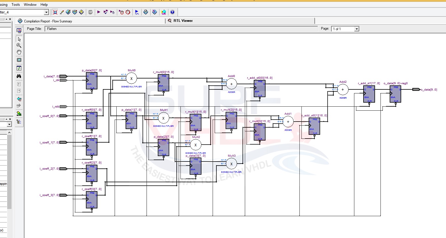
This view is a very useful sanity check to see if the compiler understood your code in the way you intended. You can see individual flip flops, adders, muxes etc... and how it wired them up. Its the best place to see what sort of optimization shortcuts the compiler has taken (It loves to reuse blocks/signals, simplify down logic, remove unnecessary logic etc...). Its pretty messy since its auto generated but clear enough to be useful with a bit of highlighting by clicking nets and blocks.
This is however still NOT how it is actually wired inside the FPGA, but simply input to the mapper that crams the functionality in actual FPGA elements. You can get a view of how the FPGA elements are wired up by opening the "Architecture view" to get a similar looking autogenerated schematic but this time with real hardware blocks in it and how they are configured. This makes it a lot more difficult to read so this view is not as useful. An even more bare metal view is the "Chip planner view". It shows you a map of the FPGAs silicon die with all of the elements inside it, allowing you to peek into each one and see how its wired up and configured. It gives you a nice view of whats is going on physically in there but is near impossible to follow signals around. It is however very useful in checking that certain blocks got configured as you expect, most useful for IO blocks in cases where you want to use special IO pin functionality like DDR, reclocking, built in serdes, delay tuning etc...
-
Brief update - have wired up the MSB RGB outputs to the VGA connector through 270R resistors to try and get some kind of output (haven't bothered with a resistor ladder to merge the LSB outputs as they're not used yet anyway). Here's the result:

Clearly an issue with sync pulses or timing somewhere... The image is a GIF, by the way, so you can see the issue if you click on the image.I wonder if the polarity of HSYNC and/or VSYNC are wrong for the chosen resolution.
Fair point - I've tried the output with reversed polarity on the hsync and vsync outputs and the monitor just goes to sleep, so it would appear the polarity is correct as I do get some sort of output currently...?You need to be sure if LINE and SCANLINES are terminal counts, or are the total number. Currently your h_counter goes from 0 to 800 (801 counts), and v_counter goes from 0 to 525 (526 lines).
Good point, I hadn't noticed that. This is where I start to make silly mistakes - basic maths.- Reset all outputs and state in the reset clause
- keep h_counter and v_counter for internal use only, and change the x & y outputs to be reg not wires.
- Keep LINES and SCANLINES as a total count, so compare to LINES-1 or SCANLINES-1 as the test for resetting the counters/
- Likewise keep HS_STA & HS_END the count where it starts, so remove the "-1" from the localparam and put it in the test.
- Try to avoid ternary operators - usage tends to be very idiomatic, so are a common source of bugs
- Unless you are careful, there is going to be ambiguity about when vsync pulse starts and ends. I suggest you testboth h_count and v_count to decide when to assert vsync. So if you want it to be aligned with the start of the visible pixels use "if (h_count == LINES-1 && v_count == VS_STA-1)" and ""if (h_count == LINES-1 && v_count == VS_END-1)" as the tests when to set the vsync outputs.
This might not give you the fastest design, nor the most compact code, but it will help you avoid lots of subtle bugs.
Okay, I've tweaked the reset clause to reset hsync and vsync as well - is there anything else I should reset in there? I'll leave LINE and SCANLINES as they are with the -1 as I'll likely be changing them in the future to regs so they can be changed by the host CPU.
As for the ternary operators comment - so it would be preferable to use full if-else conditionals instead? Is that purely because of the possibility of user error in writing or interpreting the ternary operators or because of discrepancies in how Quartus II implements them?Quote- You need to be clear about what is internal state, and what is exposed. Currently the x & y outputs feel bad.
I feel the same, I believe the sync generator should be 100% positive logic. Meaning positive hsync / vsync / an active video region output which crops the active visual area (a requirement for most DVI/HDMI serializers), and additional optional signals to trigger video timing specific events which may be fixed to the master h_count and v_count. Any visual display address / graphics /memory pointers, counters and sub-alignment positioning in the 'active video region' should be in the separate graphics image generator. Remember, a second new X/Y coordinate counter is only another 20 register flipflops max.
I popped the X & Y counters in the sync generator because it seemed like the easiest way to get some sort of graphical output at the time. Also, that's how the demo code did it that I borrowed from.
Naturally, I'm literally starting out with Quartus, Verilog and FPGAs in general, so am happy to accept feedback and suggestions on improvements.I'm waiting a day, however, I'll make a few suggestions to the ops sync generator which will solve those -1's without a -1 in the code, and solve that 1 clock delay with regards to the other variables, including the picture_enable_h and picture_enable_v signal (together = picture_enable).

@nockieboy, some questions:
1. Do you have an oscilloscope?
Yes. It's barely up to anything (and my skills using it are also pretty poor - remember, I'm not an electronics engineer and this isn't my day job!) but it's a 20 MHz Hitachi V-212. I got it cheap off eBay a year or two back when I was breadboard-prototyping my Microcom and didn't know that a logic analyser would have been far more useful.
2. Which cyclone II board do you have?
One of those cheap ones off eBay. Here's an example.3. Which version of quartus are you using?
Quartus II 64-Bit Version 13.0.1 Build 232 06/12/2013 SJ Web Edition. It was indicated to be the last version that supports the Cyclone II.4. Are you willing to use Quartus graphics design entry?
I'm certainly happy to give it a go. I'm fumbling around with Quartus II, trying to learn the ropes as I go, so I'm more than happy to find out about features like this that could help.(Not for coding, your verilog coding will stay the same, but, just to wire your verilog modules to the IO pins and potentially a few xxxx.v modules together. This will allow you to easily drop in or take out modules or remove them on the fly and see how your graphics pipe is affected as well as the CPU interface. It will allow you to easily invert IO pins, or, enable a global PLL. You can always make a now top hierarchy later-on, or, even tell quartus automatically generate you a top 'MyProject.v' verilog code of your illustrated schematic. Quartus has a feature to automatically generate a design block of each of your 'xxxx.v' source codes which you may place within your schematic layout, including multiple instances. )
Sounds very useful - I'll see what I can find out about it!
I have included my full project folder as a .zip archive for info if anyone is playing along at home. I'm not convinced I fully understand the clock setup and timing / TimeQuest Timing Analysis part of the project very well at all.
-
@nockieboy, some questions:
Yes. It's barely up to anything (and my skills using it are also pretty poor - remember, I'm not an electronics engineer and this isn't my day job!) but it's a 20 MHz Hitachi V-212. I got it cheap off eBay a year or two back when I was breadboard-prototyping my Microcom and didn't know that a logic analyser would have been far more useful.
1. Do you have an oscilloscope?
Good enough. Check the hsync and vsync being sent to your monitor. Make sure the pulse is clean and at least 4v p-p. Preferably 5v. If you are driving your monitor with a 3.3v-3.6v hsync, it may do some funny things... This is random based on the monitor's internal circuitry. If the sync it too low, IE you are driving the monitor HS/VS with an FPGA IO directly, there are 2 thing you will need to try.
1> buffer the signal through a 74HC04 inverter, or 74HC245 buffer powered with 5v. I like to drive the HS and VS into 3 gates each in parallel, and tie each of the 3 outputs in parallel to get a good current output to drive the monitor cable.
2> if the IO on the FPGA is a true 5v output, but the monitor cable load is weakening it too much, a 220Ohm to 330Ohm pullup resistor to 5v may work.
(Option #1 is better, it also separates the FPGA IO from direct connection to a wire on a VGA plug which may blow the FPGA or cause internal malfunction.)
If you use 2 channels, placing 1 probe on hsync and the second on a R/G/B pin, you should see if you get a regular pattern or not.
Also, sync polarity doesn't matter any monitor which can take in VGA with modes as high at 1280x720 or above. If your mode is not standard with wrong polarity, the monitor should potentially only have bad picture horizontal/vertical size and position unless the sync timing is not associated with the picture.
-
Check the hsync and vsync being sent to your monitor. Make sure the pulse is clean and at least 4v p-p. Preferably 5v. If you are driving your monitor with a 3.3v-3.6v hsync, it may do some funny things... This is random based on the monitor's internal circuitry.
Aha - that'll be the problem then, I'm driving HSYNC and VSYNC directly from the FPGA pins. Only R, G and B are going via 220R resistors...
My scope is showing nice clean signals on HSYNC and VSYNC, but only 3.3v p-p, which is to be expected - so the monitor is picking up some information (i.e. the R, G and B signals) but not necessarily the proper sync signals. It shows a 640x480x60 screen resolution in the menu, but as you can see from the gif I posted previously, the sync is out.If the sync it too low, IE you are driving the monitor HS/VS with an FPGA IO directly, there are 2 thing you will need to try.
1> buffer the signal through a 74HC04 inverter, or 74HC245 buffer powered with 5v. I like to drive the HS and VS into 3 gates each in parallel, and tie each of the 3 outputs in parallel to get a good current output to drive the monitor cable.
I don't have too many HC parts lying around, they're all HCT, but I'll see what I can do.If you use 2 channels, placing 1 probe on hsync and the second on a R/G/B pin, you should see if you get a regular pattern or not.
There's definitely a regular pattern - can see that on the monitor, it's just skewed and rolling because of the sync problems.
-
That picture does look like it might have some sort of HSYNC issue.
If electronics are not your main thing then you are actually doing pretty well since FPGAs are pretty far from regular programming. An oscilloscope is one of the most useful tools for debugging electronics, no other tool gives the same deal of universal insight into what circuits are doing. You do usually want to have a digital scope for digital circuits so that you can one shot capture communication buses and decode them. But video luckily involves stable repeating patterns so a analog scope can still be quite useful when triggered from vsync or hsync.
But there is a trick with FPGAs. You can build a logic analyzer in the same chip as the cirucit. Quartus has a tool for doing this called SignalTap: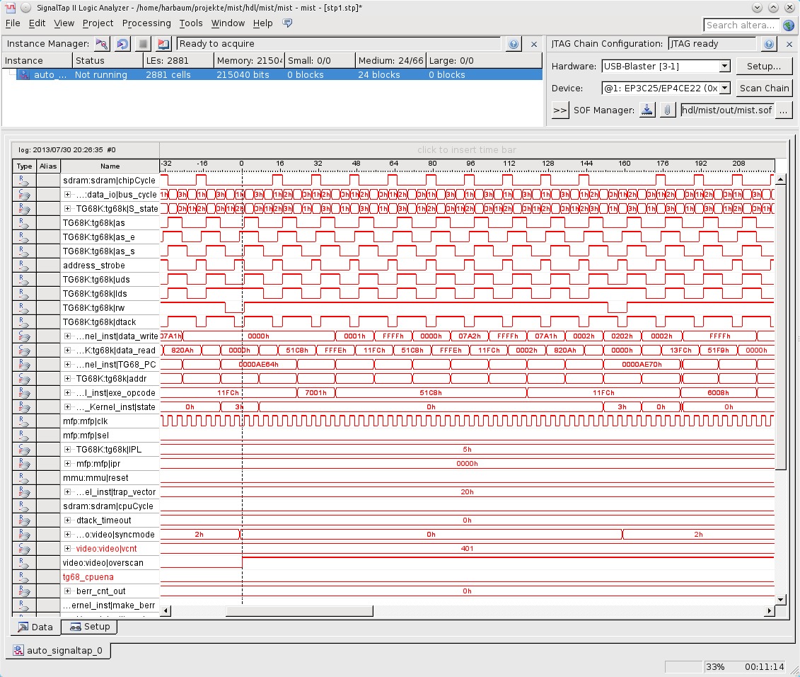
You give it a list of signals you want to monitor and how much memory to use and it generates a logic analyzer for that, taps off those signals and adds it to the design. Next time you compile your design this logic analyzer will be included in the final output and once loaded into the FPGA listens on JTAG. Then you can just click connect in SignalTap and it will allow you to interact with this logic analyzer to start captures, configure triggers etc... In some cases this is more useful than an actual logic analyzer because you have essentially 100s of logic channels available, allowing you to monitor entire counters like a bus. But because its using internal block ram means that you typically won't be making captures longer than a few thousands of samples. -
Well, that sorted the problem - thanks BrianHG!
Clearly my monitor wasn't happy with the 3.3v sync signals - I found a 74AHC541 in my box of bits and am now running the vertical and horizontal sync signals through one of these line drivers powered at 5v and am getting a nice stable output:
It's surprising how pleased I am at getting four overlapping squares to display on a monitor!!! Haha!
If electronics are not your main thing then you are actually doing pretty well since FPGAs are pretty far from regular programming.
Programming isn't my main thing, either, although I'm much better at it than electronics! Never let it be said that I don't enjoy a challenge... An oscilloscope is one of the most useful tools for debugging electronics, no other tool gives the same deal of universal insight into what circuits are doing. You do usually want to have a digital scope for digital circuits so that you can one shot capture communication buses and decode them. But video luckily involves stable repeating patterns so a analog scope can still be quite useful when triggered from vsync or hsync.
And the frequency isn't so high either - I had been using the scope originally to debug my breadboard computer running at 4 MHz, these signals are in the KHz ranges which is much more comfortable ground for my old 'scope.But there is a trick with FPGAs. You can build a logic analyzer in the same chip as the cirucit. Quartus has a tool for doing this called SignalTap:...
You give it a list of signals you want to monitor and how much memory to use and it generates a logic analyzer for that, taps off those signals and adds it to the design.
Wow! That's really useful - specially if you have a decent amount of RAM in the FPGA.
Work calls again, but when I get some more time to work on this I'll set up a resistor ladder to merge the two bits for R, G and B on the breadboard so I can try out the full colour palette.
-
Well, that sorted the problem - thanks BrianHG!
Clearly my monitor wasn't happy with the 3.3v sync signals - I found a 74AHC541 in my box of bits and am now running the vertical and horizontal sync signals through one of these line drivers powered at 5v and am getting a nice stable output:
It's surprising how pleased I am at getting four overlapping squares to display on a monitor!!! Haha! HCT is actually better for converting the FPGA 3.3v to 5v since it's inputs have a trigger threshold at TTL levels instead of mid 5v, or 2.5v. Any will work, like 74HCT, 74ACT, and other variants. (You would have never figured this one out without me. This one nearly destroyed a huge demo I had 10 years ago since my home test monitors were studio grade monitors whose sync inputs would work perfectly with a 0.7vp-p sync... The cheap PC screens didn't like that 3.3v.)
Take a day to learn how to make a top hierarchy block diagram in quartus. Make your now functioning project's 2 xxx.v files into 2 separate block and wire them on a block diagram. (Save your current project and start a new one...)
***Remember when defining the inputs and outputs. Output bus pins in quartus look like ' Red[7..0] ', not 'Red[7:0] ' like you see in verilog. It's the only BIG gripe I have with Quartus as its a drawback from their pre-verilog days of quartus 1 ... Once you are ready, I'll show you a few tricks which will make all your outputs parallel without delays, even as you add modules in-between, like my OSD character generator. I also recommend going on youtube and searching beginners guide to quartus block diagram entry, or similar to get you going. Include generating a sheet symbol for verilog source files/code in quartus...
-
For info, Grant Searle has put his site back up at searle.wales.
It seems his ISP took the site down for breach of terms and conditions due to the high traffic it was generating.
I'm trying to get my head around hierarchy block diagrams, but it's really slow going. Initially I was concerned that Quartus II 3.0 sp1 didn't support that feature, but it just seems it's deeply buried somewhere. Then I got sidetracked looking at character generators (the next big step for my design) and today, hopefully, I'll have some time to work on block diagrams again!!!
-
You should be thinking of making your own character generator, but first, you need to clean up your sync generator.
In Quartus, making a 'New' block diagram file is a key feature, not a hidden one.
Setting that .bdf (block diagram file) as the top hierarchy is also standard.
Double clicking on the the middle of the file to add pins and generic logic, or even library megafunctions is also standard.
What might be a little hidden is opening your .v file in the directory, then 'Generating sheet symbol' (I think it's called this, it's been a decade...)L:
File>Create/Update>Create symbol files for current file.
The verilog must have no errors for this to work.
Once generated, in your .bdf, double click in a blank area to add a new symbol/component. Click on user generated symbols and place the symbol on the sheet.
You should see a symbol labeled with you verilog name with all the input and output pins and buses.
In the furture, if you want to edit your verilog code for that symbol in your block diagram, you may just double click on it's symbol in your block diagram. If you add inputs or outputs and you want them to appear on that symbol in you block diagramm, you will need to re: ' File>Create/Update>Create symbol files for current file. ' to update the symbol with the new IO pins.
-
You should be thinking of making your own character generator, but first, you need to clean up your sync generator.
Yes, must try not to get ahead of myself.In Quartus, making a 'New' block diagram file is a key feature, not a hidden one.
Setting that .bdf (block diagram file) as the top hierarchy is also standard.
Sure is. Just wasn't obvious to a completely new beginner like me yesterday who only knew about creating .v files!
I found a really handy tutorial (actually a university/college worksheet) with step-by-step instructions on how to create the two types of project (one based on code, the other on a diagram), create blocks for them both and use them both in a top-level project as diagram symbols. I also learned about creating simulations, too!
This is as far as I've gotten:
Not great - I've inputs and outputs on sync_generator that don't connect to anything on vga01, which is annoying. Will go look at that.
Code for vga01.v and sync_generator.v attached for info, as I've changed vga01.v a bit to show colour bars instead of squares now.
EDIT:
Updated diagram:
EDIT 2:
From looking at this second diagram, it seems I should move the pix_en generation from vga01 to sync_generator, as it would make more sense for it to be there unless I'm likely to need it in vga01 at any point in the future there?