-
Our friends at Foveon produced a marketing graphic which illustrates light penetration through silicon.
It is my vague recollection that the depth of base and emitter diffusions in a typical "medium voltage" monolithic bipolar process is a few microns, emitters of course being shallower than bases.I'd be deeply grateful if someone who is actually properly qualified at decoding dies shots would produce an annotated version of one of the many LTZ1000 die shots kicking about marking out the actual transistors, their CBE connections and so on.
There was some speculation and links to semi-helpful sources in Noopy's original LTZ teardown thread. As an improperly qualified hobbyist I think I had figured it out at one point. See if my old posts make any sense to you.
edit
Another source, this time with concrete numbers. If I read it right, 36% of red/orange light (as seen on Noopy's photos) should be able to pass through a few microns of silicon.
https://www.pveducation.org/pvcdrom/materials/optical-properties-of-silicon
-
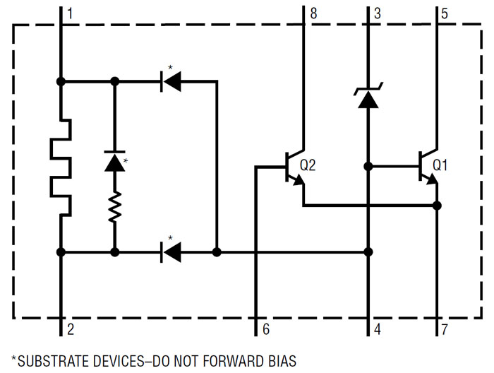
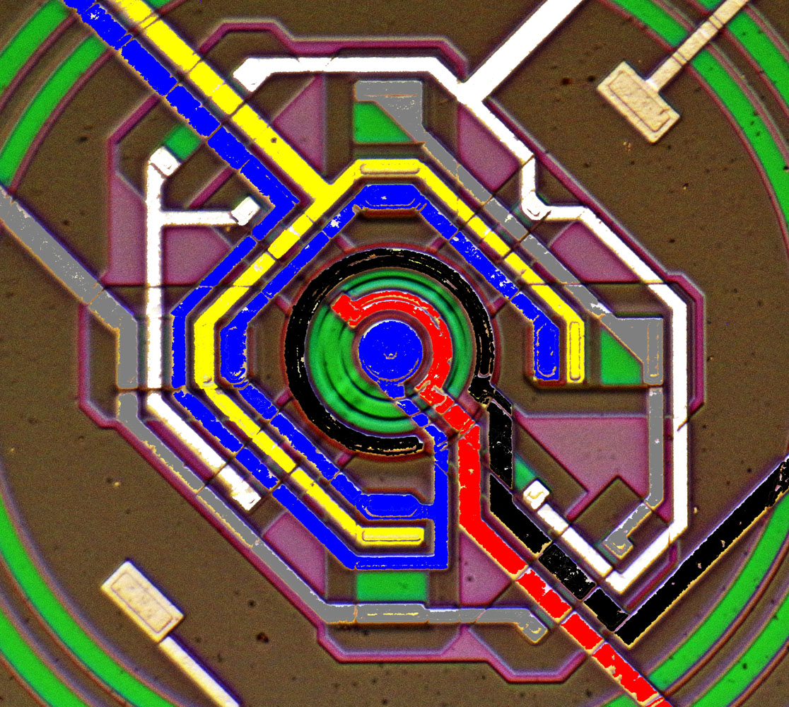
The z-diode is designed as descriped in the LM399 diagram. It is connected with the red metal (cathode) and the black metal (anode).
The transistor Q1 is already there with it´s emitter connected to the blue metal in the center. The base is a part of the z-diode (red). The collector is connected from the edge (white).
So there is a transistor which is surrounded by the z-diode but it´s already in the z-diode structure.
The "avalanche lights" confirm this: You can see the base-emitter-junction on the edge of the middle circle whereas the z-diode-junction is buried under the surrounding ring.
Q2 consists of four transistors surrounding the z-diode and Q1 (grey, yellow, blue).

Looking at a larger picture with the bonding wires I can see:
Red connects to pin 3 - Zener cathode
Black connects to pin 4 - Q1 base/Zener anode
White connects to pin 5 - Q1 collector
Yellow connects to pin 6 - Q2 base
Blue connects to pin 7 - Q1/Q2 emitters
Grey connects to pin 8 - Q2 collector
So, the Black trace connects to the Q1 base/Zener anode and Red is the Zener cathode, not as stated "The base is a part of the z-diode (red)." So the base connection is the outer circle.
My head now officially hurts from sitting here for 15 minutes trying to imagine exactly what the 3D structure of Q1/the Zener actually looks like and I'm still not there. Fortunately shopping calls so I've an excuse to give up, at least for the time being.
-
Looking at a larger picture with the bonding wires I can see:
Red connects to pin 3 - Zener cathode
Black connects to pin 4 - Q1 base/Zener anode
White connects to pin 5 - Q1 collector
Yellow connects to pin 6 - Q2 base
Blue connects to pin 7 - Q1/Q2 emitters
Grey connects to pin 8 - Q2 collector
So, the Black trace connects to the Q1 base/Zener anode and Red is the Zener cathode, not as stated "The base is a part of the z-diode (red)." So the base connection is the outer circle.
My head now officially hurts from sitting here for 15 minutes trying to imagine exactly what the 3D structure of Q1/the Zener actually looks like and I'm still not there. Fortunately shopping calls so I've an excuse to give up, at least for the time being.
Damn! I´m wrong. You are right.
You got me on a wrong track.
If I´m not wrong again my first statement was actually right: In the middle circle there is a zener with a transistor inside it. zener and Q1 share some parts but there is more inside the LTZ1000 than you can see in the datasheet of the LM399.
-
I took another look at that thing and this is my best guess of what the internal structure might be, assuming they use the standard noncomplementary bipolar process.
D1 uses the buried zener construction described in Linear AN82, but with a central hole to contain Q1. The anode consists of two P diffusions of different depth, breadth and strenght. The cathode is a strong and shallow N diffusion which fully covers the area of highest P concentration where breakdown voltage is lowest and actual breakdown will occur. This active part of the junction is located a few microns beneath the surface.
Q1 is a standard vertical NPN (top to bottom: EBC). Base is the same silicon as D1 anode, providing the necessary connection which is nowhere to be found on the surface. There is a thin, cross-shaped disturbance visible on the surface which is probably caused by a buried layer diffusion below. Such diffusion could connect Q1 collector to the four contacts surrounding the reference diode structure which are all wired to pin 5. Alternatively, D1 anode could have no hole and Q1 collector would be the N silicon which surrounds D1 anode, but then Q1 would have considerable base width and probably poor beta.
It is known that D1 anode is connected to the substrate and, according to designer Carl Nelson, there exists a subsurface Kelvin connection to the bottom of D1. I presume it all means that the anode is not isolated from the substrate by the buried layer, except for the aforementioned four thin lines. Between the lines, the buried layer is empty and the anode connects with the substrate.
A second similar ring of deep P diffusion is located outside, to isolate D1/Q1 from other transistors. This ring also is penetrated by the buried layer Q1 collector links. On its surface there is a metal connection to pin 4.
Q2 consists of four standard vertical NPNs placed around the reference structure and wired in parallel.
Comments, questions and arguments are welcome
-
I took another look at that thing and this is my best guess of what the internal structure might be, assuming they use the standard noncomplementary bipolar process.
(Attachment Link)
D1 uses the buried zener construction described in Linear AN82, but with a central hole to contain Q1. The anode consists of two P diffusions of different depth, breadth and strenght. The cathode is a strong and shallow N diffusion which fully covers the area of highest P concentration where breakdown voltage is lowest and actual breakdown will occur. This active part of the junction is located a few microns beneath the surface.
Q1 is a standard vertical NPN (top to bottom: EBC). Base is the same silicon as D1 anode, providing the necessary connection which is nowhere to be found on the surface. There is a thin, cross-shaped disturbance visible on the surface which is probably caused by a buried layer diffusion below. Such diffusion could connect Q1 collector to the four contacts surrounding the reference diode structure which are all wired to pin 5. Alternatively, D1 anode could have no hole and Q1 collector would be the N silicon which surrounds D1 anode, but then Q1 would have considerable base width and probably poor beta.
It is known that D1 anode is connected to the substrate and, according to designer Carl Nelson, there exists a subsurface Kelvin connection to the bottom of D1. I presume it all means that the anode is not isolated from the substrate by the buried layer, except for the aforementioned four thin lines. Between the lines, the buried layer is empty and the anode connects with the substrate.
A second similar ring of deep P diffusion is located outside, to isolate D1/Q1 from other transistors. This ring also is penetrated by the buried layer Q1 collector links. On its surface there is a metal connection to pin 4.
Q2 consists of four standard vertical NPNs placed around the reference structure and wired in parallel.
Comments, questions and arguments are welcome
Chapeau! Good explanation, good picture, very nice!
Sound reasonable!
...how did you paint this?
-
...how did you paint this?
A few circles, rectangles and 45° rotations to get one quarter of the top surface, then mirror to get a full half, then perspective transformation. All functions available in gimp, I'm sure other advanced image editors like Photoshop could do it too.
The cross section is just a few ellipses drawn on a new layer which restricted them to the bottom half of the frame. That's cheating; frankly, the base diffusion should have a flat bottom over most of its area
It actually is pretty simple in retrospect but I spent an hour learning how to operate that crazy software. -
A vector drawing application like Adobe Illustrator, or Inkscape in the open source world, would be perfect for that kind of work!
Photoshop will work, but it has to be flogged to go there, kicking, screaming, and protesting the whole way... (It has only rudimentary vector drawing capabilities). I have never tried the Gimp but I imagine it doesn't major on vector drawing eiter. Photoshop is to Illustrator what Gimp is to Inkscape, I believe. -
I used zero vector graphics capabilities and drew it like in Microsoft Paint

Yes, I know. But vector graphics would be yet another even more specialized software to learn. Raster editors are more versatile; everything I did today I will probably want to do to a photograph or some bitmap graphic downloaded from the Internet another day. In the past I used Gimp to alter schematics in PNG format, try that with a vector editor
-
wow, I was under impression that the picture was made in a chip design CAD.
-
I used zero vector graphics capabilities and drew it like in Microsoft Paint
Yes, I know. But vector graphics would be yet another even more specialized software to learn. Raster editors are more versatile; everything I did today I will probably want to do to a photograph or some bitmap graphic downloaded from the Internet another day. In the past I used Gimp to alter schematics in PNG format, try that with a vector editor
I hear you. These applications have big learning curves. But there are really only those two fundamental types... if we ignore 3D for now!
-
Here's a paper describing light emission from a silicon avalanche diode. Fantastic to see those pictures.
https://aip.scitation.org/doi/10.1063/1.4931056 -
wow, I was under impression that the picture was made in a chip design CAD.
No. I'm not a professional designer, just spent too much time staring at analog ICs
The drawing is to be taken with a grain of salt. It may be wrong altogether and various minor details are certainly wrong.
It's completely not to scale, in real world the deep diffusions are almost half-spherical because the dopant doesn't care which direction to diffuse, the concentration of dopant steadily decreases as it diffuses further away from the point of application which I didn't bother trying to show, the shallow diffusions ought to have flat bottoms because the "point" of application is not a single point or line but a wide 2D area, possibly other things... -
However I doubt that one would see light from the buried junction. This would be rather deep inside the silicon so only very little of that light can escape.
I´m not sure about this.
A view days ago I tried to use a big KD501 transistor as a photovoltaic cell.
(https://richis-lab.de/Bipolar02.htm)
Across the base-emitter-junction I got the same current as across the base-collector-junction. It seems there wasn´t significant light reduction.The normal avalanche process should also not produce light as the energy from the hot electron is used to generate new pairs. The normal recombination in silicon is without any light and if any it would be in the IR range (~ 1 µm). It would be only if a hot electron recombines or excites some defect in some way.
I agree with you that hot electrons generate new pairs but some of them will recombinate. Otherwise you will get a real breakdown with 0V and destruction of the junction. (I´m not absolutely sure about the last sentence but that would be my interpretation.)
The hot electrons can have a higher energy than you will see while normal current flow in the semiconductor. With "normal" current flow and "normal" recombination you don´t see any light. I agree with that. But in my view there is recombination of hot electrons.
I tried to take a "maximum tilted" picture but you can´t really say where the light is generated: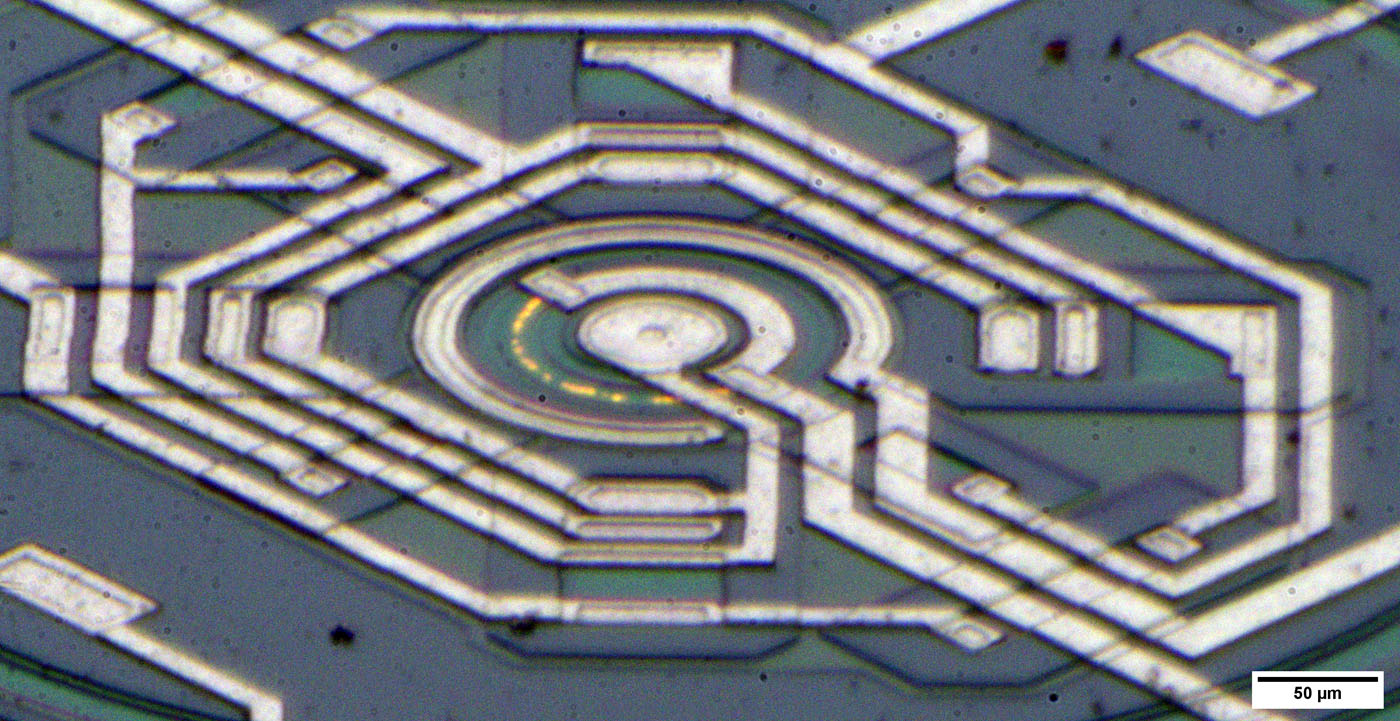
Hi all!
We talked about the avalanche breakdown light in the LTZ1000 and whether it is generated in the pn-junction. If so the light dots would stand for irregularities in the zener-junction.
Kleinstein suggested that the light dots occur in the upper layer at impurities outside the zener-junction.
Coincidentally I got a BUX22. What is the similarity between the LTZ1000 and the monster BUX22?
The BUX22 has some minor but visible defects in the base-emitter-junction:
And the glowing occurs first next to the defects not on top of the defects. In my view that means that the avalanche breakdown glowing occurs first at points where there are irregularities in the pn-junction (higher electrical field force).
q.e.d.
Whole story here:
https://richis-lab.de/Bipolar07.htm
-
1. I don't think that this project would belong into this thread, please delete and continue with your other one, you already opened.
2. Concerning the LTZ1000, why do you want to reinvent the wheel, again?
Maybe you should define precisely your requirements concerning stability figures and noise immunity, before discussing cosmetic aspects like the form factor, and (again) over-engineering the components used. Better than A9 and compact designs are already available.
Frank -
Point 1 is well made, but how is re-using the A9 "reinventing the wheel", quite the opposite surely, and there's nothing cosmetic about form factors.
A form factor is a basic utilitarian part of a specification - there's a world of difference between a portable instrument and one intended for rack mounting. Form factor is probably point one on any outline specification for any product, so much so that the form factor implicitly or explicitly defines whole categories of products. Nobody wants a toilet that doesn't fit the implicit form factor, or a 50 cm mobile phone, or a 2.5 m long 'luxury' car. -
1. I don't think that this project would belong into this thread, please delete and continue with your other one, you already opened.
Not the A9 from a 3458A, but an LTZ1000 reference in a A9 form factor, electrically compatible (better resistors, lower running temperature, better layout). What do you mean by reinventing the wheel? One can never have enough LTZ1000 projects or references. I haven't built one yet, why shouldn't I? I don't want to use an existing one, I don't like the form factor and the layout of the existing ones, simple as that, they are awesome piece of engineering don't get me wrong, I'm don't doubt the performance one bit, but don't fit my philosophy and needs. All the requirements are around the form factor, if compromises need to be made, they will be made to fit the form factor. Completely agree on the requirements, this is high level, not well thought yet. Considering VHD200 as overkill for an LTZ1000 project in my opinion is questionable, I certainly don't agree with it. We don't have to continue discussing, as this indeed does not fit the LTZ1000 thread, you are very welcome to jump on the other thread
2. Concerning the LTZ1000, why do you want to reinvent the wheel, again?
Maybe you should define precisely your requirements concerning stability figures and noise immunity, before discussing cosmetic aspects like the form factor, and (again) over-engineering the components used. Better than A9 and compact designs are already available.
FrankPoint 1 is well made, but how is re-using the A9 "reinventing the wheel", quite the opposite surely, and there's nothing cosmetic about form factors.
I wholeheartedly agree with this, thanks a lot
A form factor is a basic utilitarian part of a specification - there's a world of difference between a portable instrument and one intended for rack mounting. Form factor is probably point one on any outline specification for any product, so much so that the form factor implicitly or explicitly defines whole categories of products. Nobody wants a toilet that doesn't fit the implicit form factor, or a 50 cm mobile phone, or a 2.5 m long 'luxury' car. -
Here is some data on an LTZ1000 ref I've been playing with, this does not look very good does it?

-
Here is some data on an LTZ1000 ref I've been playing with, this does not look very good does it?
Any RF sources nearby? Neonlights on the ceiling? If you have a spectrum analyzer, please check of any unwanted RF. -
It is hard to tell how good the LTZ1000 reference is. With a DMM reading the DC voltage one sees a combination of the external and DMM internal reference. With the DMM7510 this is the LTFLU and LTZ1000 combined. Depending on the DMM setting one may also have some extra contributions from the DMM (the DMM7510 has relatively high noise at 100 PLC - seems to be some odd Keithley specific thing).
So some 1.8 µV peak to peak is about the value one would expect. Naturally the noise reading show quite some variations. A reliable noise reading takes quite some times, so more like the median over some 10 intervals with some 100-1000 readings. -
The DMM7510 isnt capable of displaying the actual LTZ-noise, for that youll need a 0.1-10Hz-LNA.
Id suggest to use batteries instead of a powersupply for such measurements.
Also the graph-function is limited by the 4LSB-noise, maybe it gives out more resolution via GPIB which can be used to produce a better/smoother diagram? -
Here is some data on an LTZ1000 ref I've been playing with, this does not look very good does it?
Frankly speaking, your whole set-up, including the cables, is not looking good at all.
I also do not know, what's inside the aluminum sheet, or what your LTZ reference you're actually using.
Anyhow, you're always comparing the LTZ versus your DMM, so the noise is always a combination of both.
Your instrument should perform noise-wise nearly as good as a 3458A, the whole setup seems to have too few resolution, at least the rms noise for an LTZ is on the order of 200nVrms or 0.03ppm only.. maybe you also use Standard Deviation for measuring the noise.That 1.7µV pp is not optimal, but on the order of what to expect.
If you want to have stable measurements, you're really dealing with sub-ppm stability - what a properly built LTZ can deliver, you have first to set up everything in a stable way, not that Flying Dutchman approach.. these loosely hanging, un-shielded cables with inappropriate connection jacks are simply acting like antennas, and by themselves create a lot of other disturbances.
If your actual LTZ circuit (?) is built from the original LT schematic, then it's not inert at all against E.M.C., so the hint for SMPSUs from others, is the crucial point here.
Maybe you understand now, that 'better' components, layout, and so on are not the key points.. maybe you just do the basics first.
I will append a picture how the stability diagram will look like.
Frank
-
Yes! The thing on the wall just next to it is a low energy Bluetooth device measuring temperatureHere is some data on an LTZ1000 ref I've been playing with, this does not look very good does it?
Any RF sources nearby? Neonlights on the ceiling? If you have a spectrum analyzer, please check of any unwanted RF.
-
It is hard to tell how good the LTZ1000 reference is. With a DMM reading the DC voltage one sees a combination of the external and DMM internal reference. With the DMM7510 this is the LTFLU and LTZ1000 combined. Depending on the DMM setting one may also have some extra contributions from the DMM (the DMM7510 has relatively high noise at 100 PLC - seems to be some odd Keithley specific thing).
Yes I know that
So some 1.8 µV peak to peak is about the value one would expect. Naturally the noise reading show quite some variations. A reliable noise reading takes quite some times, so more like the median over some 10 intervals with some 100-1000 readings. This is not a serious measurement, just a sanity check. Three or more multimeters (DMM7510 and 3458A) sampling the reference is what I had in mind for the serious measurement, and proper cables and shielding.
The reference used here is an old and unmodified A9 board from an 3458A. DMM7510 is what I had conveniently located near the power supply. -
Yes I know that
This is not a serious measurement, just a sanity check. Three or more multimeters (DMM7510 and 3458A) sampling the reference is what I had in mind for the serious measurement, and proper cables and shielding.
The reference used here is an old and unmodified A9 board from an 3458A. DMM7510 is what I had conveniently located near the power supply.
That's a too elaborated approach, which will create new problems.
Parallel measurement with several DMMs is unnecessary, complicated, and will give big interference noise from one DMM to the other.
We had this failure recently, during our MM 2020 already, so do not repeat the same mistake.
Keep everything simple, i.e. one good DMM, make a clean setup, do the basic shielding, and then you're done.
Frank
https://www.eevblog.com/forum/metrology/volt-nut-meeting-2019-in-stuttgartgermany/msg3091382/#msg3091382 -
Am I the only one that doesn't see any problem?
niner_007 -> ΔY = 1.73uVpp (unkown interval)
Dr. Frank -> ΔY = 1.33uVpp (** 1 hour interval)
(** assuming 7V absolute value, and +/- 0.95ppm Δ)
So results doesn't seem too bad considering power cables, and board and DMM placement.