-
Hello Emmanuel,
While there are some 24-bit DACs on the market, most of them do not perform anywhere near 24-bits in reality, resolution is just that, nothing more, beyond 20-bits it is just noise. The closest DAC I know that exceeded 20-bits was built by Jim Williams in Linear's AN86. This accurately measured 1 PPM with linearity to 0.1PPM, while it is not overly complicated, it required more than just one chip but it worked quite well. http://cds.linear.com/docs/en/application-note/an86f.pdf
I am not entirely familiar with the AD5491 but any ADC/DAC over 16-bits in real accuracy is no easy matter to make and at 20-bits, it really is pushing state of the art for accuracy. Most anyone can achieve resolutions of high numbers, but resolution has very little to do with accuracy or repeatability and math cannot improve what is not accurate to begin with, as we say in computers - garbage in garbage out.
With my 242D resistance bridge, I can achieve up to 11 digits of resolution and to some extent I can repeat to 10 digits at least, however at best, in absolute accuracy I can 'only' achieve ~1PPM accuracy with an uncertainty of ~0.2PPM at best, therefore I usually will not give a calibration reading that exceeds the 7th decimal place at best because the rest of it is only resolution and it is known to not be accurate. It is nearly impossible to match this accuracy with any other method of measurement, there are too many variables involved and uncertainties to even approach 1 PPM accuracy otherwise. -
Hi Emmanuel,
The only 24-bit DACs I can find are all audio types, not really any good for DC, there are a few current units, the AD1852, CS4398 and PCM1789 to name a few of them. I could not find an AD5491 but I did find a AD5791 which is a 20-bit accurate DAC from Analog Devices, kind of expensive as expected and is rated for DC operation. Its specifications are very close to the multi-chip DAC that Jim Williams designed.
Getting back to the Vref subject, I found some rather interesting information from the NIST about the ohm, concerning the quantum ohm standard, it can only be read with an uncertainty of 0.2PPM at best, no matter what national lab in the world it is, all agree on this uncertainty. Furthermore, this uncertainty is not included in calibration certificates as it is understood by all labs that it is there, all uncertainties provided on the certificate of calibration are in addition to this 0.2PPM. The document is here:
http://www.nist.gov/customcf/get_pdf.cfm?pub_id=31431
It also provides other information about the process of calibrating primary standards, uncertainties and the bridges/methods used.
Another interesting document is the calibration pricing sheet here: http://www.nist.gov/calibrations/resistance.cfm
You can get your SR-104 certified to the best accuracy in the world for only $3.385,00 plus shipping.
Another very interesting tidbit of information from the NIST about solid-state Vrefs: if it is an LTZ1000/A or LM399, the design should be using PWW resistors if you want the results to mean anything when you get the device back. They will tell you that right up front and to get that Vref certified, $2206 covers a couple measurements per day over 12 to 15 days, then they send you the average result. Cost to ship it back is $519 to you and they would prefer that the device is battery powered for a minimum of 30 days but they will provide up to 50 watts of mains power if it has to be plugged in.
The calibration pricing for Vrefs of various types can be found here: http://www.nist.gov/calibrations/voltage.cfm
As usual there is more information on voltage standards and particularly the solid-state references.
And that gentlemen, is why I do not send my standards to the NIST, I use a primary certified lab who paid the big bucks up front to the NIST and can provide almost identical uncertainties in their readings at a much lower cost, not that it doesn't cost a lot, it just isn't in the thousands of dollars.
Note the comment on DVMs and other similar instruments on this page.
Regards,
Edwin -
Re. linearity of PWM and other DACs, I think you are misising the point. 20 bit e.g., which is available, equates about 1ppm resolution. That is good enough to adjust a voltage reference (even with bad DNL/INL).
The real issue is, what is the stability over time. If it is good (Including all its resistor and opamp drifts), then a 20bit DAC is a good solution. -
You can get your SR-104 certified to the best accuracy in the world for only $3.385,00 plus shipping.
Calibration Uncertainties for Low-power DC Resistance Standards
Nominal Uncertainty ( 95 % confidence level )
NPL (UK) NIST (USA)
100 uohm 2.5 ppm 4 ppm
1 mohm 0.85 ppm 1.2 ppm
10 mohm 0.8 ppm 0.8 ppm
100 mohm 0.18 ppm 0.5 ppm
1 ohm 0.06 ppm 0.3 ppm
10 ohm 0.05 ppm 0.3 ppm
100 ohm 0.05 ppm 0.2 ppm
1 kohm 0.05 ppm 0.2 ppm
10 kohm 0.06 ppm 0.2 ppm
100 kohm 0.08 ppm 0.8 ppm
1 Mohm 0.12 ppm 0.8 ppm
10 Mohm 0.2 ppm 3 to 8 ppm
100 Mohm 0.4 ppm 5 to 12 ppm
1 Gohm 1.6 ppm 10 to 25 ppm
-
Hi folks,
Sorry for double post, but since DAC topic was discussed in this derailed thread, I'd like to get some comments on AN86-based voltage generator I'm trying to make.
Thread with schematics for discussion.
Thanks! -
@ Itz2000,
First, the documents linked to were dated 2003 and 2004, so they are a little out of date, should be newer documents on the NIST website.
Secondly, the uncertainties/accuracies quoted in the document ares what the regular, run of the mill calibrations are done to, it is not the actual capabilities of NIST. By appointment only, NIST will certify a standard to a higher accuracy than the standard rates quoted in the document and that was noted in the documents. I know for a fact that NIST can read the national 1 ohm standards to PPB, in fact they state that the average drift of their primary group of 1 ohm standards are drifting by .0046PPM/year compared to the international legal ohm standard (SI). They use the same DCC bridge techniques as other national labs do, in short, the NIST absolute accuracy to the SI ohm is as precise as any other national laboratory, including the British, of which you so kindly listed their current uncertainties. This said, the SI ohm standard is still no better than the 0.2PPM uncertainty to the quantum ohm which is known to all national labs and is the current legally defined absolute 'ohm' standard.
The secondary calibration labs, the ones who service most of industry, including my standards, all quote similar accuracies and uncertanties given in the NIST documents for regular level of certification, anything better than that is considered special as noted in the documents. The British and likely all other national labs will have the same tier of certifications as NIST. Calibration to these levels of accuracy and uncertainty is no trivial matter and a national lab will not do special certifications for just anybody.
So I still stand by my statement that the NIST is as good as it gets.
As far as I know, the absolute accuracy and uncertainty of resistance standards are of no consequence to anyone on this blog except possibly me since I must adhere to resistance certifications in order to build accurate resistors, I know precisely how accurate my SR-104 is and my 242D bridge. The fact that someone may own an SR-104 does not mean they are also as accurate without the proper bridge equipment, DVMs are not standards. Vishay must also adhere to the same requirements, except that they have a habit of buttering their specifications, which has nothing to do with their calibration lab. I have not seen or read any comments directly from another resistor house here.
-
Sorry folks, to interrupt:
you're wondering about the 0.2ppm SI / absolute / Klitzing Ohm...
It's quite easy, and still actual, as somebody else already mentioned:
Currently, the SI Ohm is uncertain to about 0.2ppm only!
Same goes for the SI Volt!
That's due to the current definitions (from 1990) and/or mise en pratique, derived from other SI base units, like the kg, frequency, length, and several "unprecise" constants of nature.
Best mise en pratique of the Ohm (in terms of SI units) is the Thompson-Lampard capacitor ( calculable capacitor).
The Ohm is NOT defined or derived from the Hall / von Klitzing standard; at the moment latter one is ONLY the best way to have a repeatable, site independent standard.
The von Klitzing constant for the Hall effect resistance (combination of e and h) currently is an approximation only, also 0.2ppm uncertain relative to the SI.
Therefore,the absolute uncertainty as per today can not be any better than these 0.2ppm, nowhere!
Therefore, the NIST declaration is very reputable..
In 2018, probably a new SI will be adopted:
The kg will be defined by the silicon sphere and/or by the Watt balance.
Several constants of nature will be defined with zero uncertainty, especially h and e.
As a consequence, the Ohm and the Volt, defined AND mise en pratique by the Klitzing and the Josephson quantum effects/standards, will also have zero uncertainty!
That means, that both effects are already proven to be 1e-17.. 1e-19 stable or reproducible on cryogenic level. (That is: SQUIDs for null detection, superconductivity, no thermal voltages)
That will be as stable as the second / frequency quantum standards (Hg or Al optical clocks).
The problem to connect these cryogenic standards to the real world, will still be persistent.
The difference between both worlds are thermal voltages of the order of several nV, which limit the achievable real world uncertainty to about 1e-8.. 1e-9, but that will be 1 or 2 orders of magnitude better than before.
What's lacking also, are working / secondary standards for Ohm and Volt, being as stable as << 1e-7.
Therefore, even when the new SI 2018 will be gone into effect, there will be no big improvement in practice, as we will certainly still discuss the stability / T.C., etc. of PWW and BMF resistors...
Frank -
Below is die picture of LTZ1000. I did noticed that 4 inner heating elements are not used and only the two outermost are used.
Do you have any idea why?
One bond wire ( pin 6) torn.
I will follow up with more voltage references die images ( on my desk are prepared VRE3050,VRE310, LT1027) but it will be more difficult digging than die of LTZ1000.
Teardown of LTFLU can be also interesting, but I did not find any cheap or not working on ebay yet ;-)
Thanks TiN for providing sample.
-
Cool! Can you drop a high resolution version as well?
I think using further heater coils help with less gradient across active components. You dont want creating hotspot around zener parts. -
I will try to make better image without charging artifacts later.
If you do not mind I can make cross section. It looks like that reference is OK except pin 6.
Here is limit for upload 1MB :-( Full image is about 1GB.
To reduce gradient there is symetric design, I was really surprised how symetric layout is.
Additioal heating elements can be also for higher temperature or who knows different elements are used on LTZ1000A vs LTZ1000.
Do you remeber if it was A version or non A?
Also I have no idea why pin 7 is connected above burried zener in centre... -
thermal dummies, you want heat to radiate out isotropically, are you sure all the heaters are not used, i.e. multiple layer connections for whatever reason? also, thermal conductors/heatsinks to increase thermal capacitance at that area maybe, so heating is more stable (thermal filter).
-
thermal dummies, you want heat to radiate out isotropically, are you sure all the heaters are not used, i.e. multiple layer connections for whatever reason? also, thermal conductors/heatsinks to increase thermal capacitance at that area maybe, so heating is more stable (thermal filter).
There is no via visible, two wires from pin 1 are connected to two from six outermost heating elements and third pin 1 bonding wire is connected to layer below two outermost elements. -
Notice that this die is a 1988 version, so it is one of the earlier dies and Linear may well have 'tweaked' it further since then. The date is right next to pad 2 in the photo. It is also not unusual for a die to have additional 'components' which are or are not used depending on the version being manufactured.
-
You can upload here any size you want at my host. I will do size processing and rehost as bunch of smaller pics.
It was LTZ1000A from 2013, bought from LT direct shop.
I posted photo of it in my KX thread before: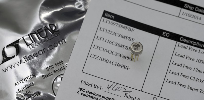
-
To Ken: Thanks for info! So I do not understand why there is visible probing on unused heater pins. It looks like thay are at least measuring them prior contacting the die in package.
To Edwin: Date on die is 1983, due to bad stitching setting it looks like 1988 :-) Sorry
To TiN: So it is prety recent unit. Do you remember whats went wrong with unit? Or it is only pin 6 issue? -
I'm pretty sure wirebond 6 was damaged due mechanical when sawing a can.
Issue was that after some countless experimentation with resistor and opamps it refused to give correct output zener voltage, and provided almost 13V output, and
was taking must more current than normally should do (>50mA). I suspect it was due incorrect heater setpoint, which caused die to overheat way over 100°C.
This was very first LTZ I got, so it was a sacrifice for learning curve. 5 units after it still working like a charm
-
Mmmm... looks like I came to the right place for information on this.
0.0005%/C is way more than needed for my purpose and temperature range -55deg to 100deg means the "S curve" is nowhere near as short as hinted earlier. At least in the ball park with initial tests (0.1mv) on some homegrown zener parts I've been tracking for last couple weeks.
Prices for USR, 1n829, and 1n939 are more than an LM399 so just as out of reach as the LTX1000 for my budget so it looks like the DIY parts at 2 cents each are for me. I hope performance of cheapies is close enough. The circuit looks a lot more manageable to compared to LTZ too which is another plus. Even simpler because I don't need negative ref. I got OP07s but maybe not even any op amp will be needed if ADC ref input impedance is high and I use software calibration constants.
If you *REALLY* want to go down this road, take a look at the LT1034:
http://www.linear.com/product/LT1034
Bit late to this party, but the LT1021-7 is cheaper and comes with a built in regulation circuit very similar to the unheated LTZ1000 reference design.
BTW, aren't most discrete zener diodes subsurface? The Motorola/OnSemi manual for discrete zener diodes mentions a "drive in cycle" which puts a passivation layer on top of the junction. -
Definitively no:
A glass passivation of a surface zener is not the same as a ion implant subsurface zener.
And also you cannot compare the (long term) stability of the LTZ1000 with that of a LT1021
With best regards
Andreas
-
A glass passivation of a surface zener is not the same as a ion implant subsurface zener.
I only asked if the zeners weren't all subsurface.
"The resultant junction profile is determined by the background
concentration of the starting substrate, the amount of dopant
placed at the surface, and amount of time and temperature
used during the dopant drive-in. This junction profile
determines the electrical characteristics of the device.
During the drive-in cycle, additional passivation oxide is
grown providing additional protection for the devices.
After junction formation, the wafers are then processed
through what is called a getter process. The getter step
utilizes high temperature and slight stress provided by a
highly doped phosphosilicate glass layer introduced into the
backside of the wafers. This causes any contaminants in the
area of the junction to diffuse away from the region. This
serves to improve the reverse leakage characteristic and the
stability of the device. Following the getter process, a second
photo resist step opens the contact area in which the anode
metallization is deposited."
The glass passivation is a different step.QuoteAnd also you cannot compare the (long term) stability of the LTZ1000 with that of a LT1021
No, but you can compare it to the LT1034 which was being suggested as a low cost source of a buried zener diode ... if you just want a cheap'ish buried zener reference without resistor divider the LT1021-7 provides that. -
Hi, Been away a few weeks. Got to make a living

Latest measurements: Temperautre sensing transistor of the LTZ1000.
- Had 0.1mA over them for about a minute ( ((7.1-0.6V)/70K) = 0.093mA ) base-colector to emitter
- Room temperature 24.3C
- Eight different ICs from the same batch
Result:
Average of the eight: 0.6027V (ie very near 0.60V at 25C)
Max-to-min value of the eight, 6.2mV, equivalent to 3.1C
All for today... -
Can you guys make a small how-to step by step to do your test? I can measure my 4 references. I can supply 100uA from 2400 SMU.
-
Hi,
What you can do is simply apply 7.1V over a 70K or 68K collector( (Plus) to emitter(7) (minus), tying base(6) to collector (. Nothing else connected. You can use standard 1% resistors. Sketch attached.
Then measure voltage over collector-emitter. Measure room temperature.
If you have had your fingers on the LTZ1000, let the temperature of the LTZ1000 stabilize for several minutes.
You can measure Q1 in the same way tying positive collector(5) and base (4) and measure to negative emitter (7)
I have the privilege of having a source-meter, then it's simple....
-
I have both A and non-A units.
So if I use SMU then just supply 7.1V with 100uA compliance, no need for 70K resistor, correct? -
Hello,
I would not rely on a 100uA current from a SMU.
Usually leakage currents of power stages are in the 0.1-1mA range (per transistor).
So I would use 7.1V (perhaps limited to 1mA) + the 70K resistor.
With best regards
Andreas -
I have both A and non-A units.
If you trust the SMU, go ahead, that's what they are for. Mine has read-back for current / voltage, separate of the set point. Never had issues with it.
So if I use SMU then just supply 7.1V with 100uA compliance, no need for 70K resistor, correct?