-
Thank you very much!

You probably don't want to hear me speaking english.
-
I have another 2"-wafer for your:
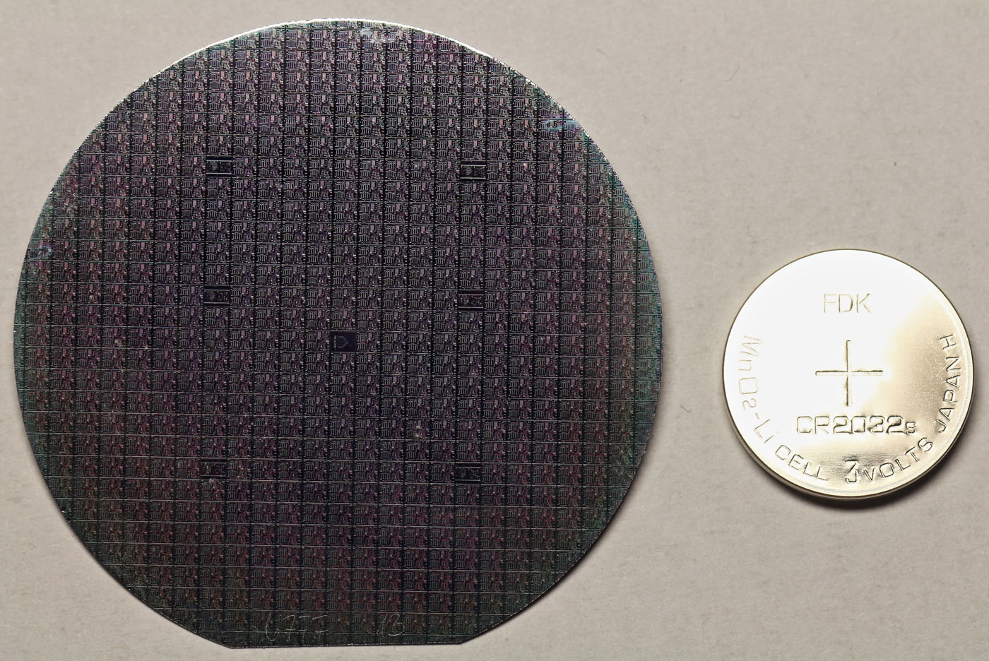
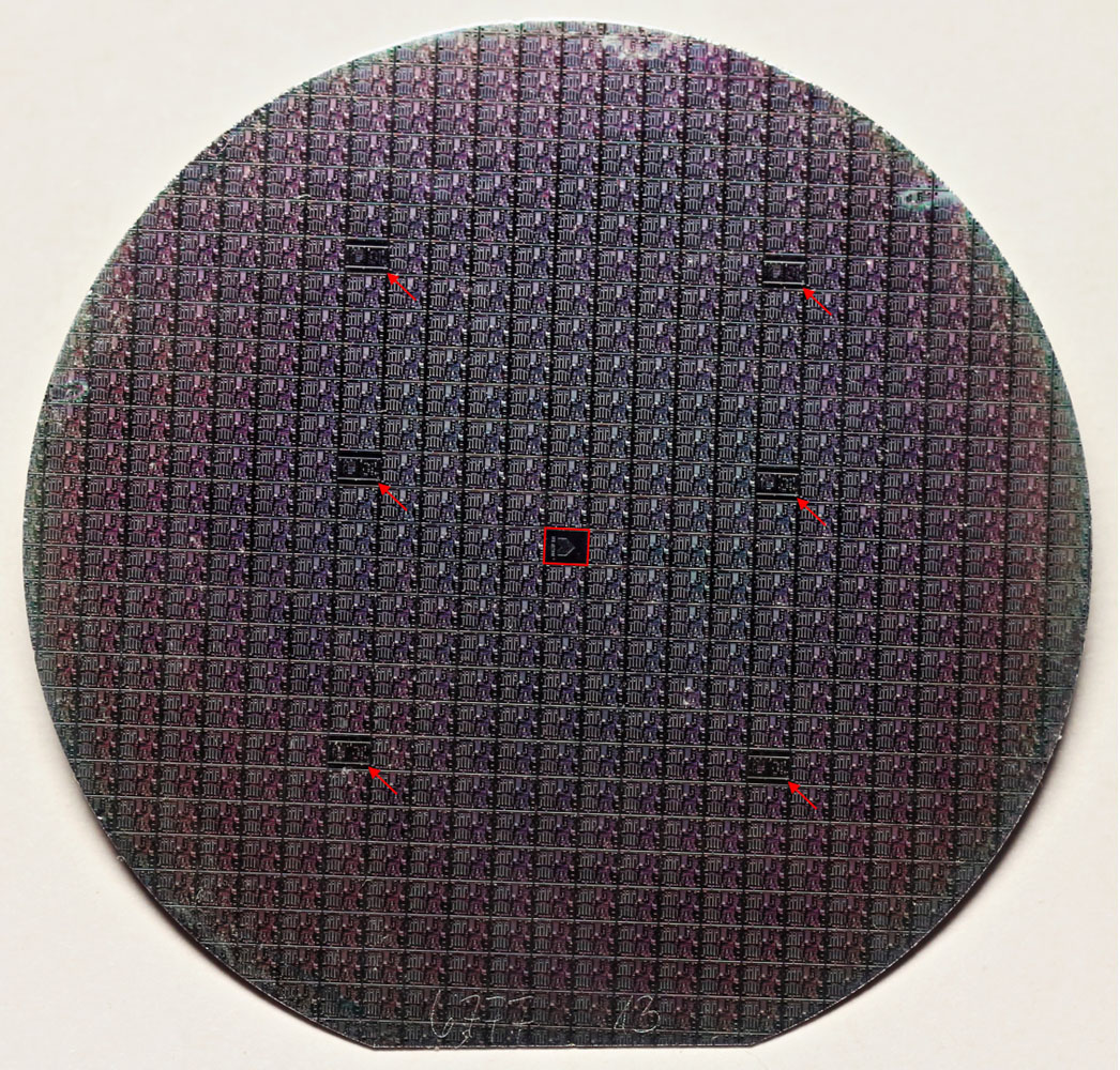
Four test structures to check the process quality.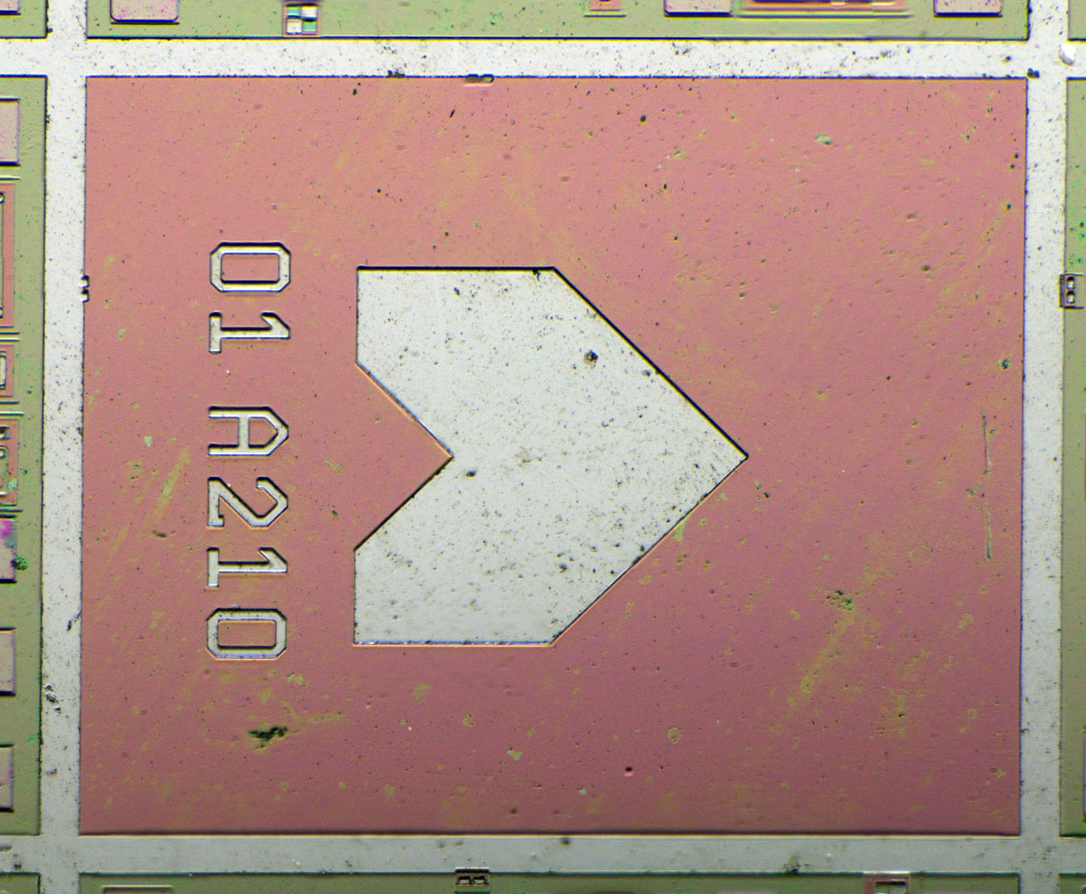
Aha, a A210-audio-amplifier! ...I wouldn´t say HIFI...

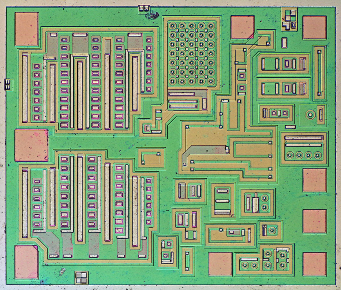
The metal layer is missing like on the D220-wafer. You can´t check the whole circuit but you can see a lot more of the active devices.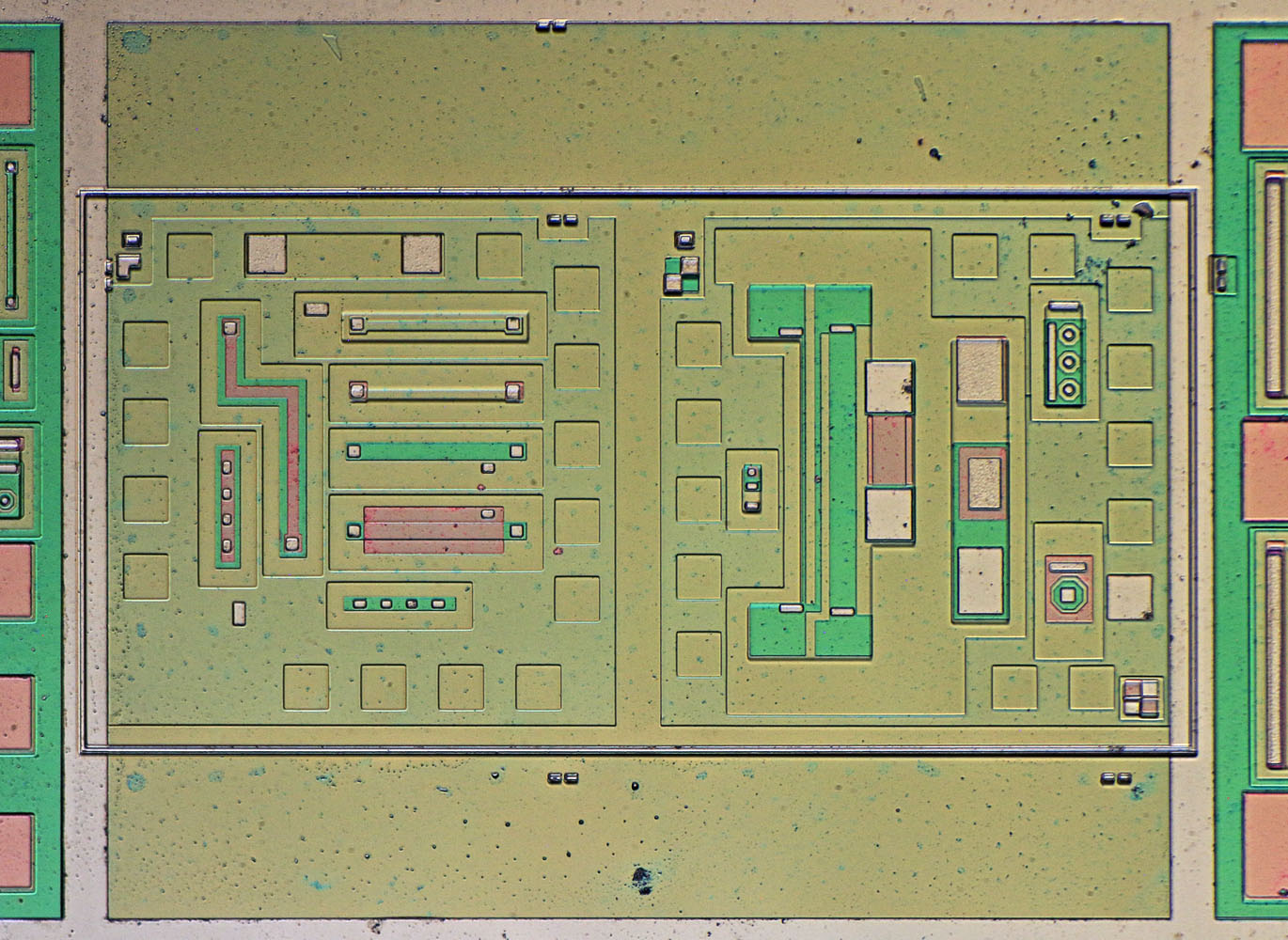
 It look´s like they used two test structures that where designed for smaller dies and combined them on one die of this wafer. Now the frame extends to the milling area.
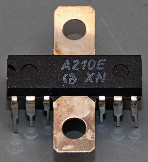
That is how the A210 looks like with it´s suit on.
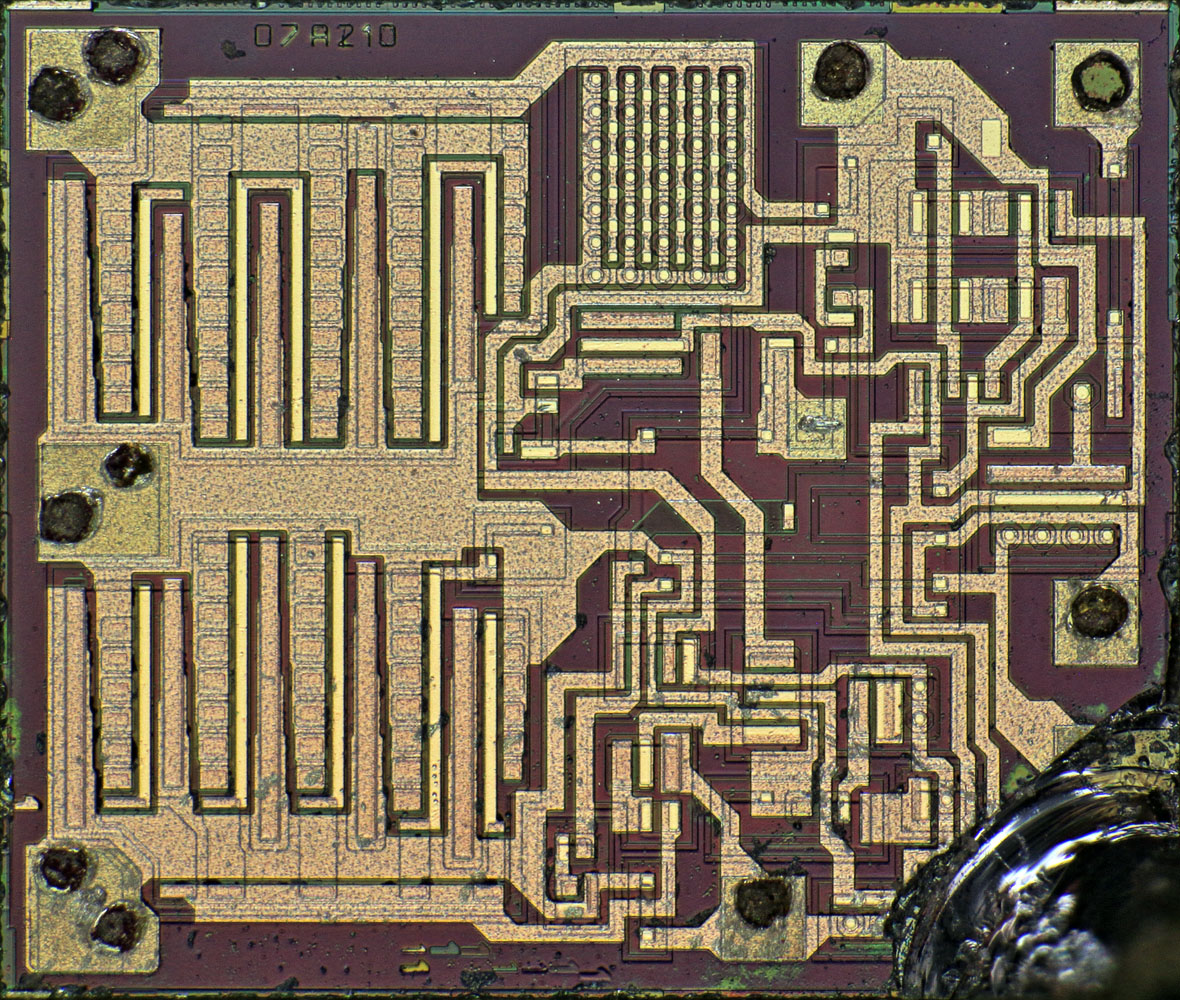
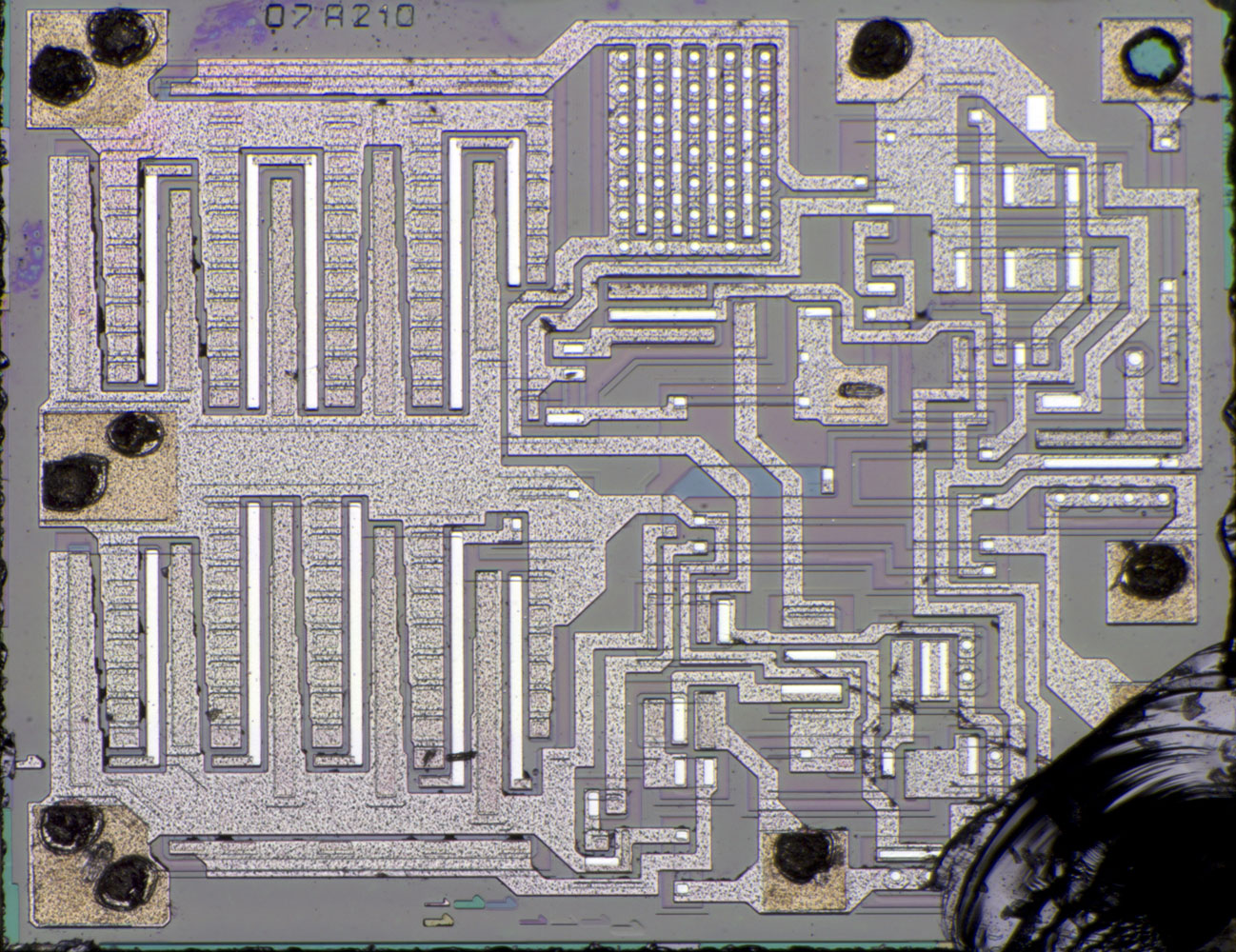
Sorry, I damaged the die...
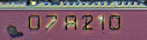
Revision 07... They had a lot of homework to do.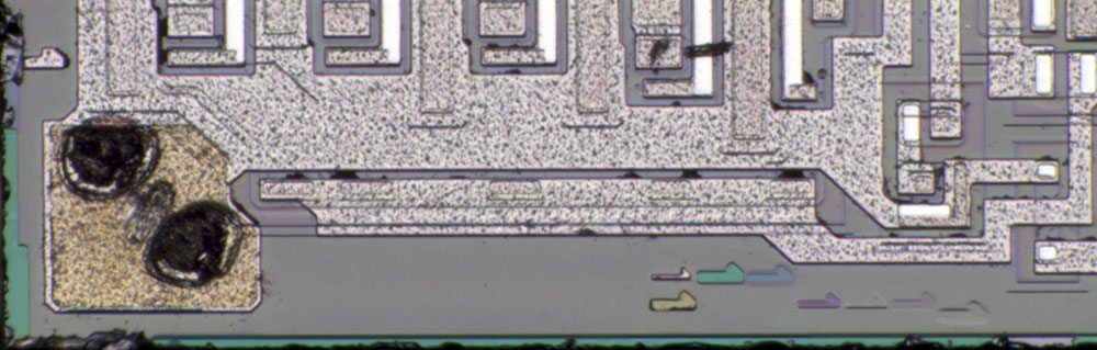
And later they added mask revisions.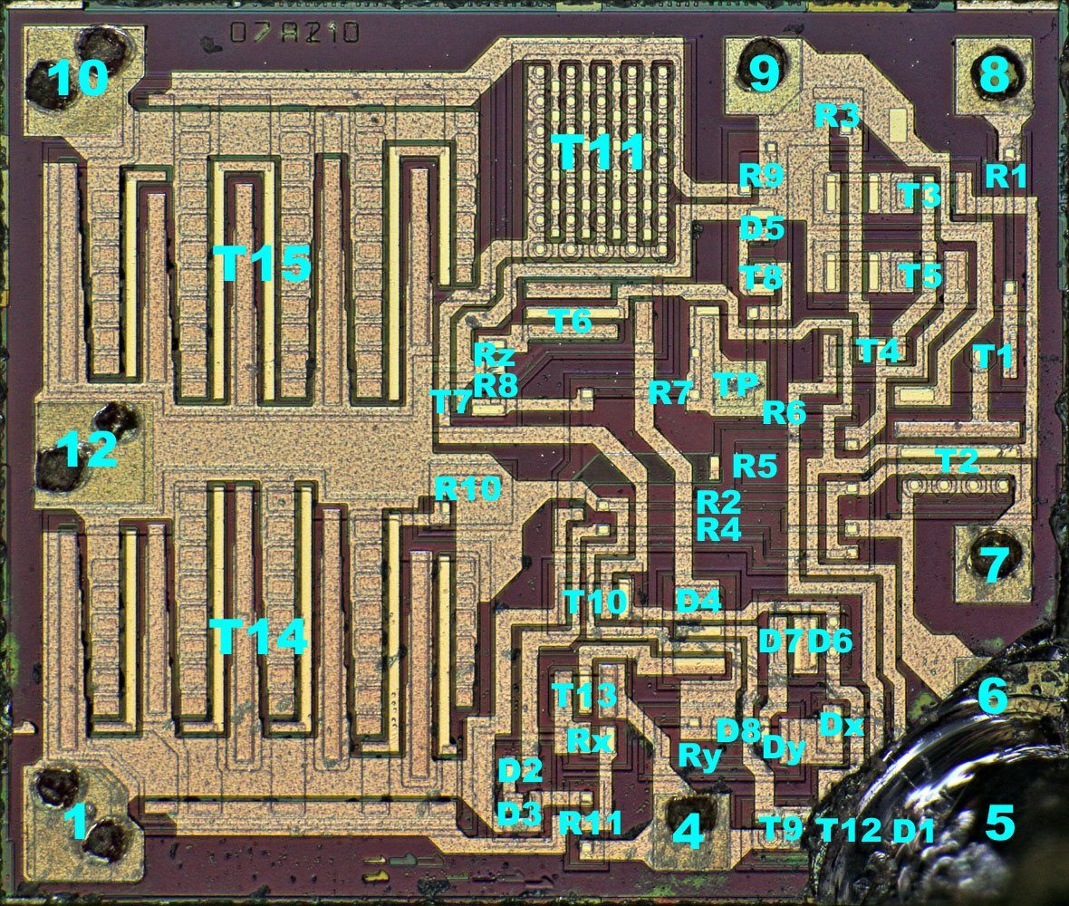
Most parts can be found on the schematic. But they added two small emitter resistors and...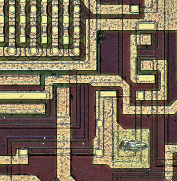
There is a testpad for checking the overtemperature shutoff. So they didn´t have to check the amp at high temperatures.
And there is the possibility to change the connection leading to a different resistance of R7 leading to a different overtemperature limit.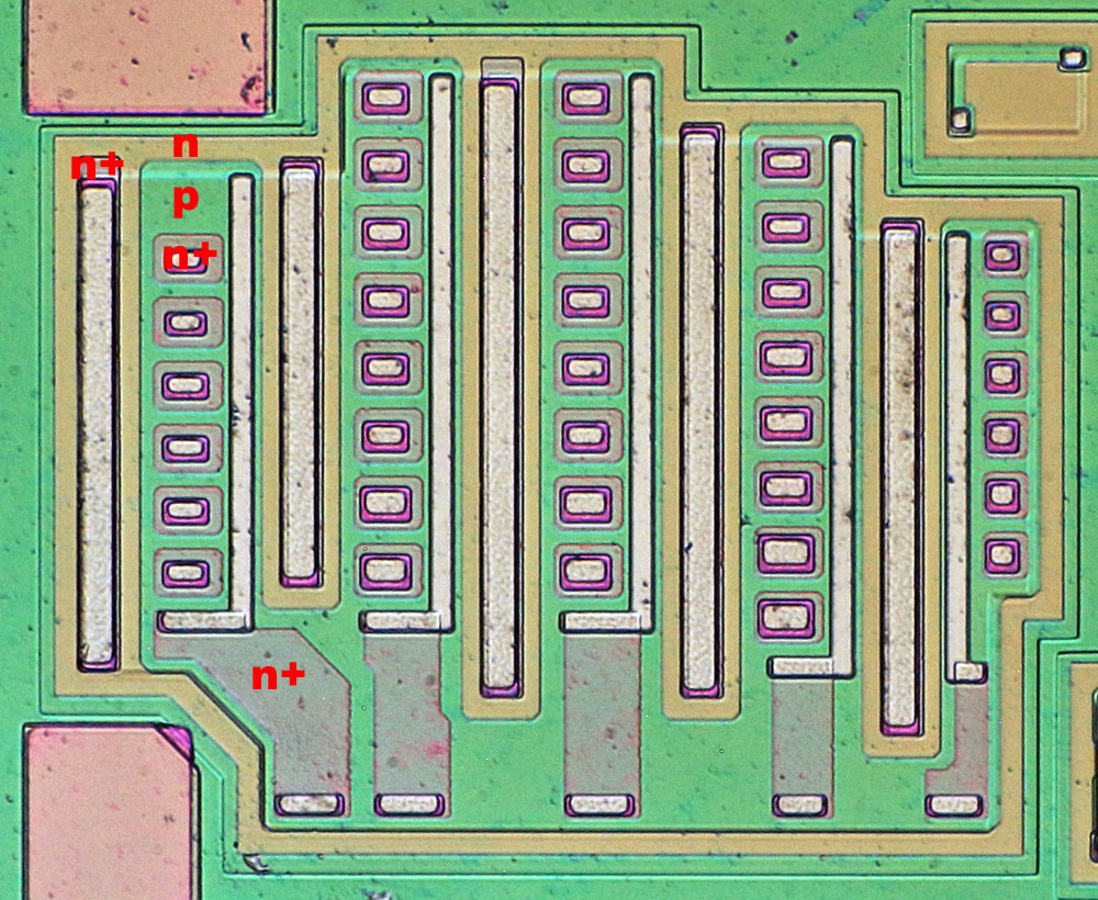
A nice big output stage transistor.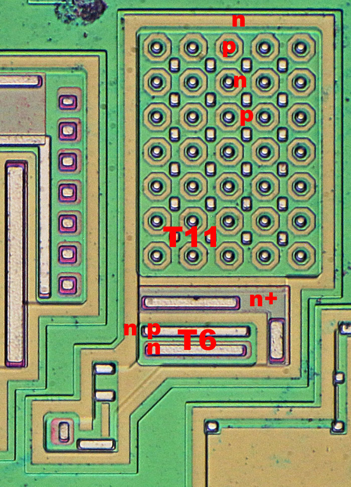
These lateral PNP-transistors are quite bad. You need a lot of die area to get good enough specifications.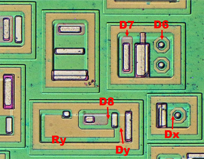
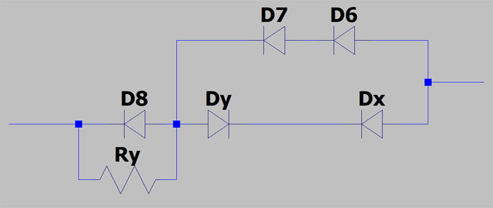
They added a resistor and one or two diodes to the bias circuit of the output stage... I´m not sure why...
More pictures here:
https://www.richis-lab.de/wafer02.htm

-
Good old fashioned quasi-complementary... yeah, that would be a pain in the days of lateral PNP.
Tim -
A little bit more modern, the TDA7396: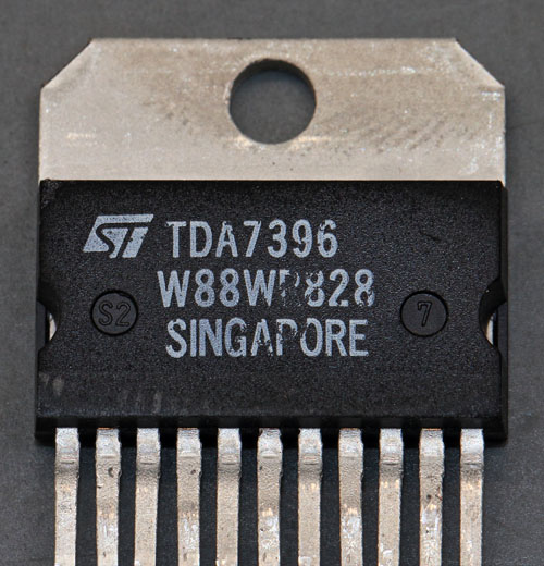
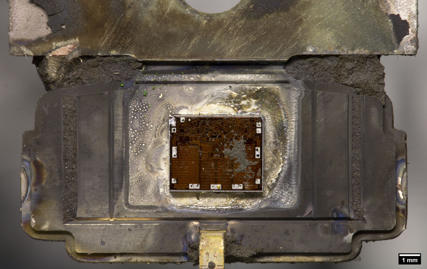
The die is 4,71mm x 3,79mm.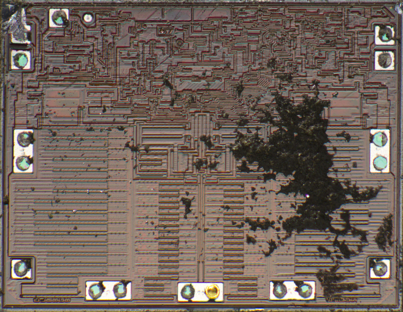
I don´t like these polyimid coatings, they need very high temperatures to deteriorate...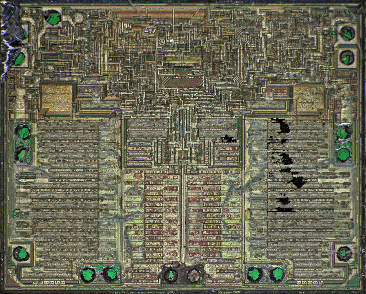
...often the metal layer is damaged while heating it to the higher temperatures.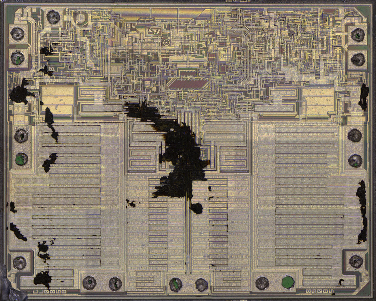
But I managed to get a good picture.
The TDA7396 uses two metal layers. The circuit is quite dense.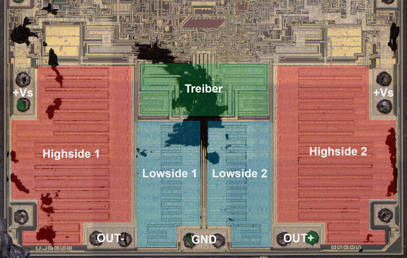
The H-bridge transistors can be identified easily.
-
Today I have the Mikroelektronika Botevgrad CM630, a 6502-clone:


I can identify the information in the instruction ROM!
https://www.richis-lab.de/prawez04.htm -
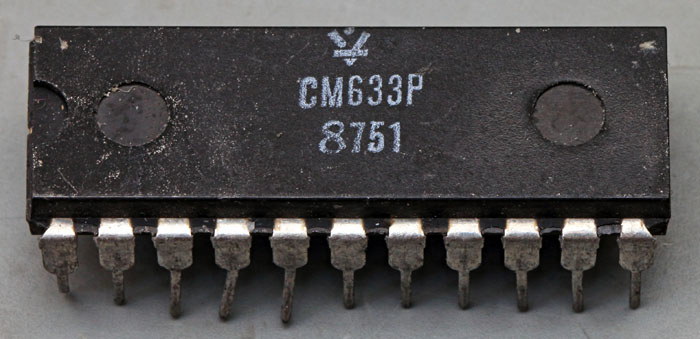
The CM633 is a 16R8-PAL built by Mikroelektronika Botevgrad and used in the prawez computers simliar to the Apple 2.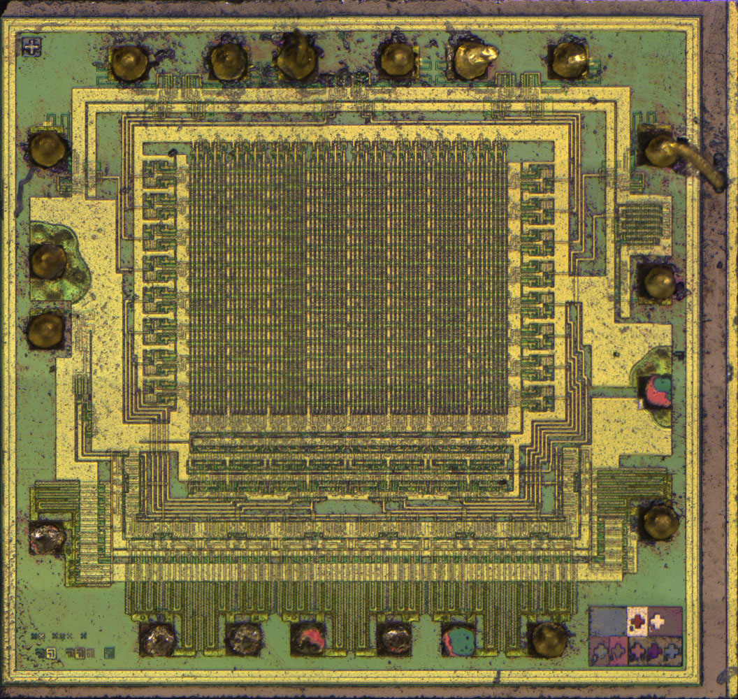
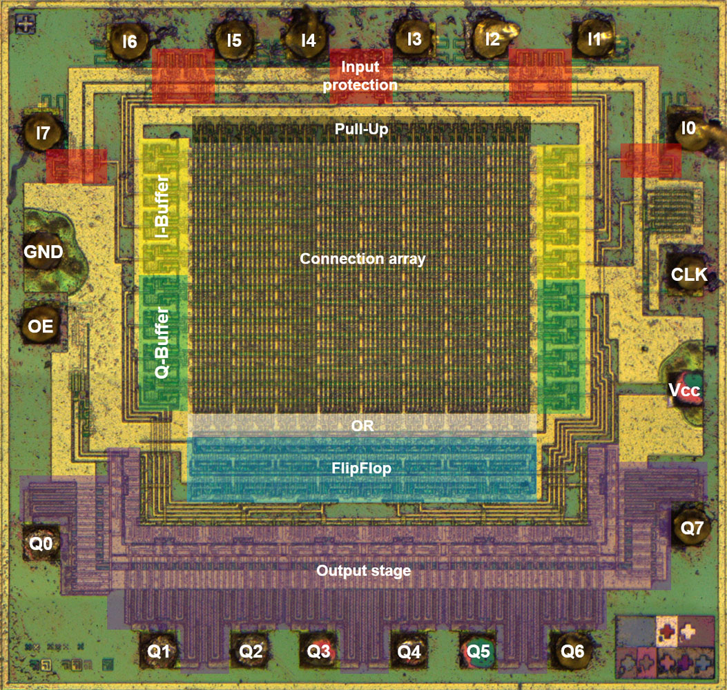
The die pictures are not perfect but it´s possible to find the functional blocks.
The structures are very small but it looks like one can see the status of the antifuses in the array.
https://www.richis-lab.de/prawez05.htm
-
Update: The CM633 is a HAL not a PAL!
With more magnification you can see the vias connecting the metal layer with the active area.
(The picture in the last post is updated due to hotlinking.)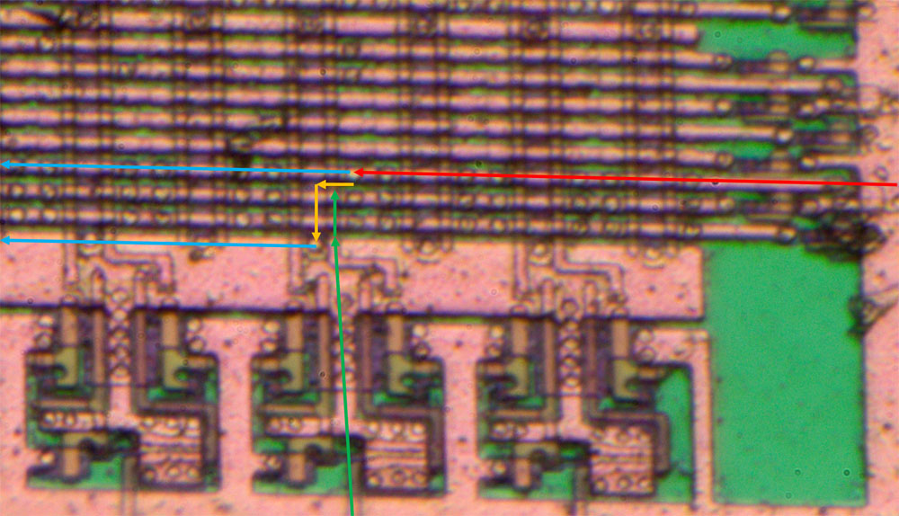
You can see that there is no simple electrical connection. Eacht metal line is equipped with a pull-up (red). Each control line (green) forms a transistor between a via and a ground line.
-
The 0127 is a strange injection interface. I don´t know very much about this asic.


https://richis-lab.de/ECU02.htm
-
Let´s look inside an old 2,1W-Sanyo-amplifier: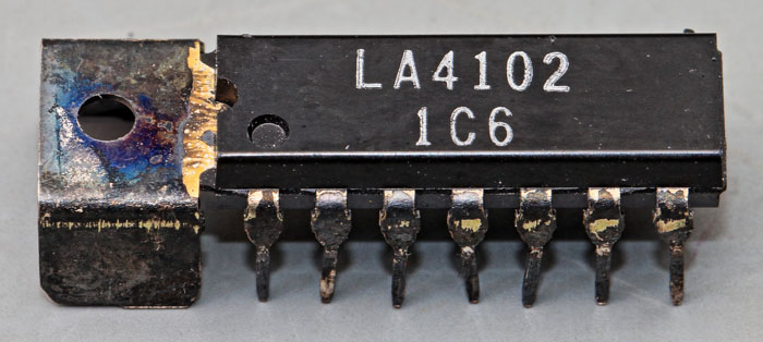
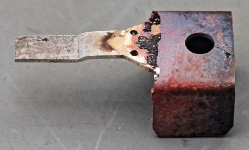
The heatsink sheet carries the die.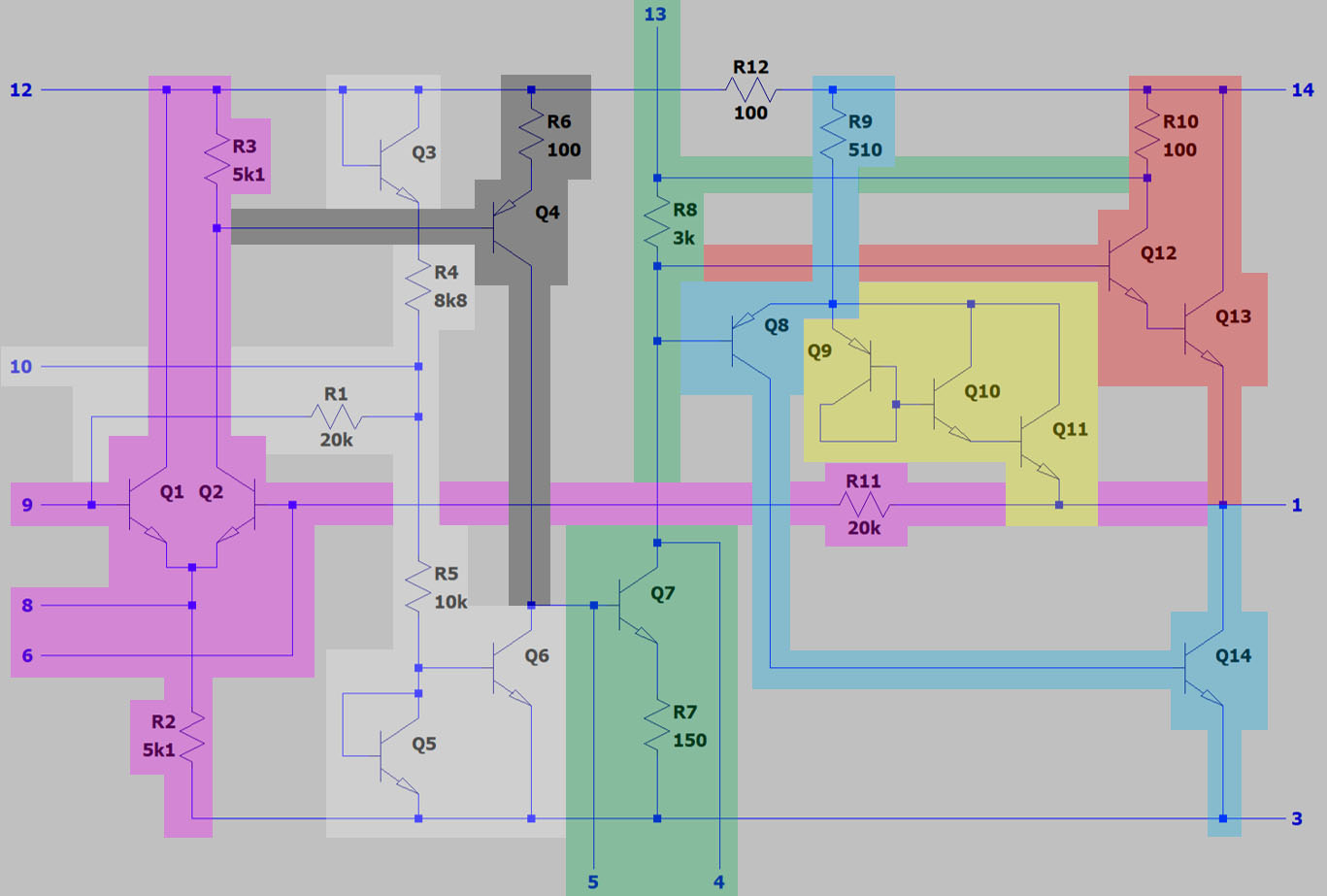
Between the differential amplifier (pink) and the VAS (green) there is an additional amplifier (dark grey). This amplifier is shifting the signal and unloads the input amplifier.
In the VAS there is an internal and an external feedback path.
An interesting point is the bias generation of the output stage (yellow). The bias is based on the output and causes some current to flow through the lowside Transistor. That causes current through the highside. Nothing special but at high output levels you can switch of the highside completely. That´s good because of the small supply voltages.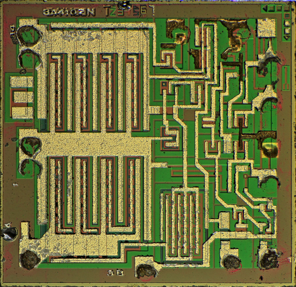
Nothing special, but...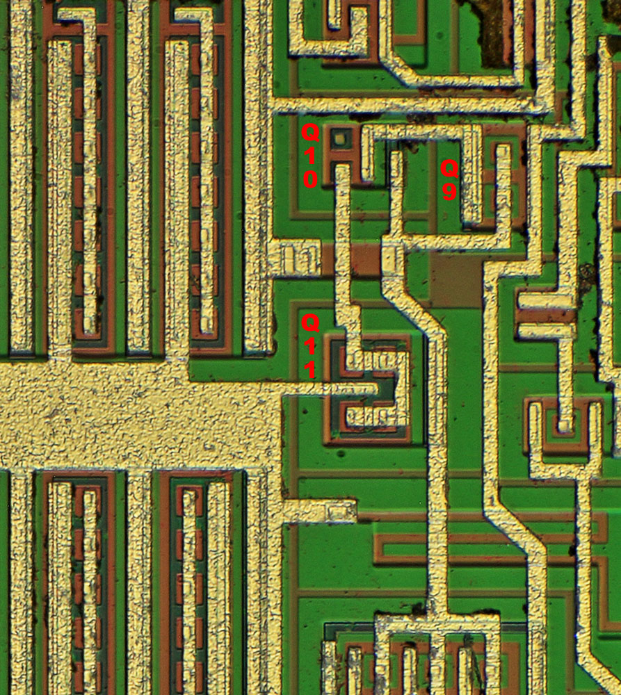
...the output transistors and the transistor Q11 are built with a perforated emitter! The dark grey emitter is not put in squares but in a grid that contains holes to contact the base area underneath. That´s interesting!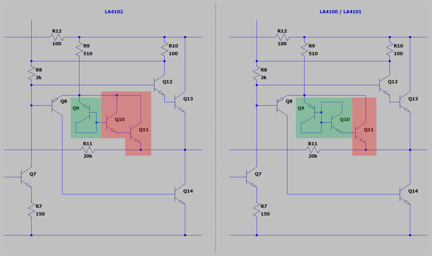
Another interesting point: The LA4100 and the LA4101 are specified with lower supply voltages and less output power. But these amplifiers are no selected parts. The bias generator is connected different so that the bias in the LA4102 is less than in the LA4101/LA4100. I assume they had to do this to lower the power dissipation. -

The Interdesign 2438 is used in engine control units as a front end for inductive rotation sensors.
Well, nothing special to see...
https://richis-lab.de/ECU03.htm
-
They sure needed a lot of resistors in that one!
Tim -
They sure needed a lot of resistors in that one!
That´s for sure!
Today I have a CM8116 for you. It´s a 16kBit-RAM manufactured by Mikroelektronika Botevgrad:
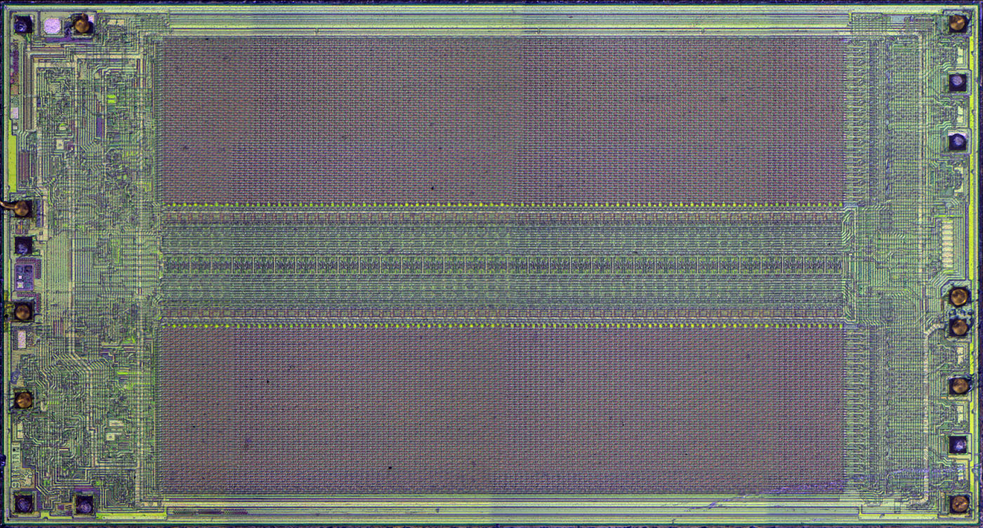
They needed 5,7mm x 3,1mm for the 16384 Bits.
But what´s that? It´s an ITT 4116!
A nice elephant!
Some more pictures here:
https://www.richis-lab.de/prawez06.htm
-
Today I have a part of a wafer for you:


It contains the A3520, a SECAM-decoder similar to the TDA3520.
More pictures here:
https://www.richis-lab.de/wafer03.htm

-
I just wanted to point out that I have built a calender presenting some of the best pictures of 2020:
https://www.meinbildkalender.de/richis-lab
If you are interested...
-

Does anyone of you know which manufacturer hides behind this logo? It´s on an analog digital converter...
-
One more audio amplifier:

LM380, single supply 2,5W @8

The input is built so you can use a input signal with ground reference without a coupling capacitor. Absolut maximum ratings ist +/-0,5V at the input. I assume that degrades the signal a little bit. With every negative mV you get more leackage current over the substrate.
In the input there is a pi-type differential amplifier. One leg is used for negative feedback.
The VAS (green) is also the predriver.
There is some additional potting on the die. Getting rid of this potting was not easy.
It took a lot of heat to get to the silicon.
1,6mm x 1,4mm
The output amplifier is built with darlington transistors.
The datasheet states an overcurrent protection. You can´t see a shunt measurement over the emitter resistors. It seems like the two circuits on the left are doing the overcurrent protection. But how does the circuit detect the overcurrent? Thats no MOSFET output stage in which you could built a current mirror current measurement.
The first transistor of the input also is built with a Darlington configuration 1a/1b and 2a/2b.
https://www.richis-lab.de/audioamp03.htm
-
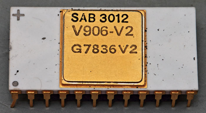
SAB3012 - TV remote receiver and memory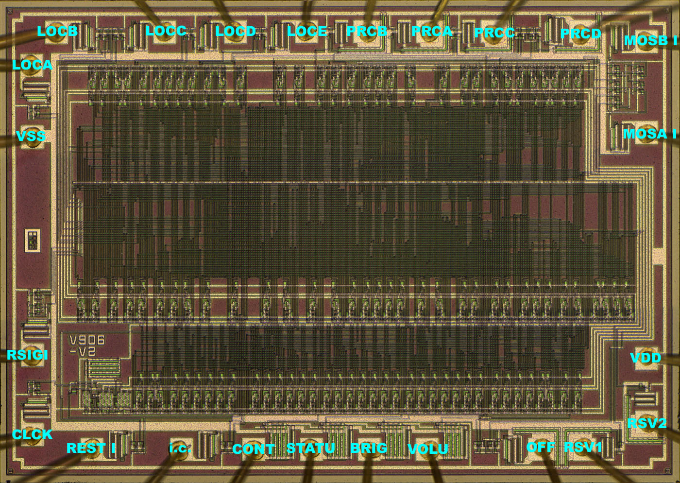
Most of the area is occupied by the logic. I assume the three stripes are the memory for the four "analogue" outputs. In fact the outputs are digital but with a RC-network generate a analogue signal.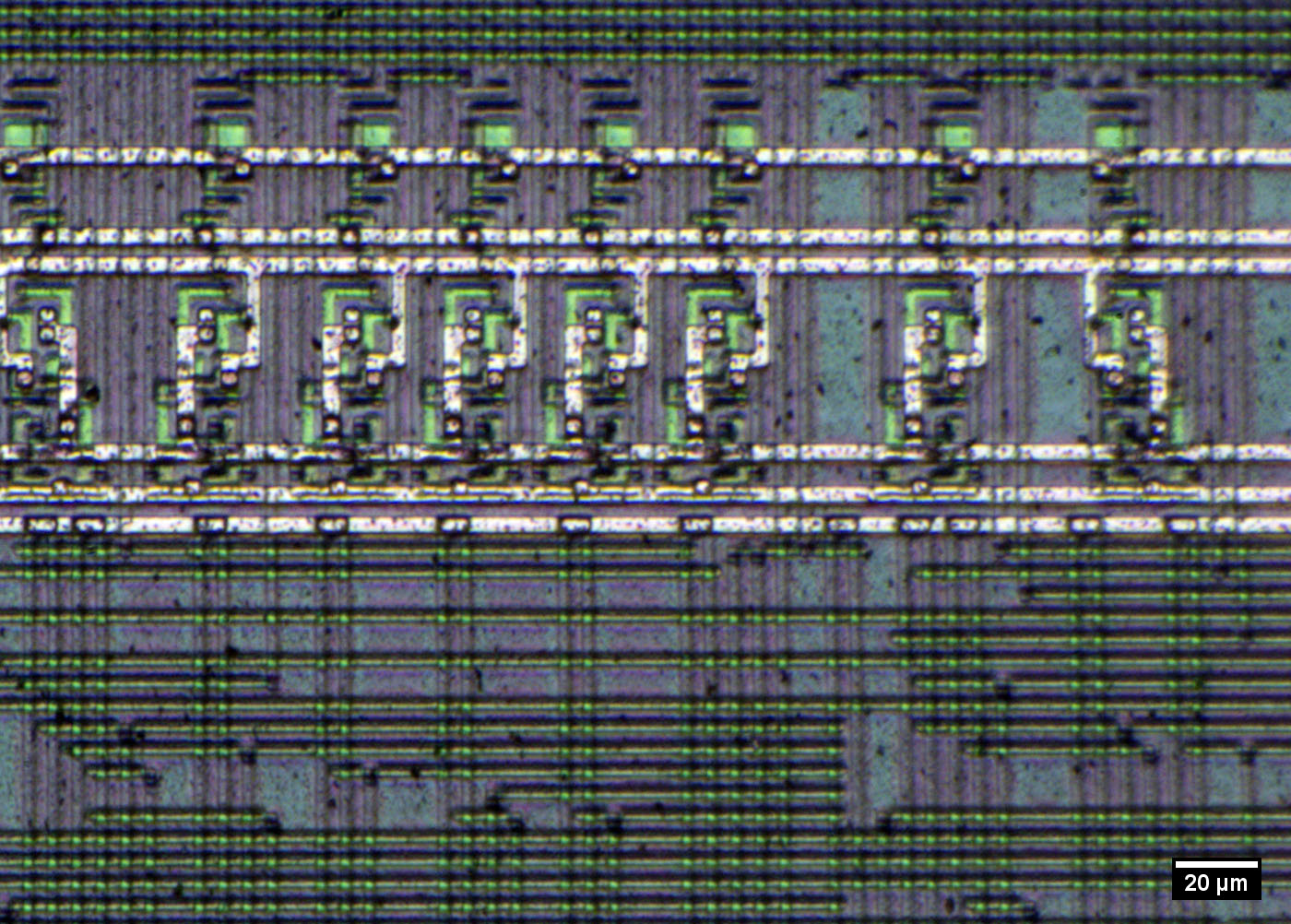
Although the crossing of the lines looks uniform it has to represent transistors and connections...
https://www.richis-lab.de/SAB3012.htm
-
Let´s take a look into an old hall-switch:

The B461 was built by HFO in 1983.
They used some gel potting to protect the die.

The hall-effect occurs under the metal square in the silicon. The metal square probably acts as a shield against electrical fields.
More pictures here:
https://www.richis-lab.de/hall01.htm
-
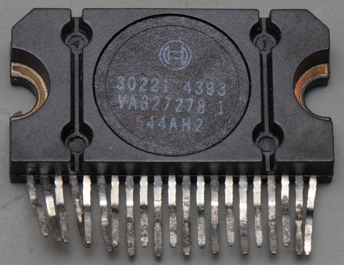
The Bosch 30221 is a sixfold lowside switch used in motor control units.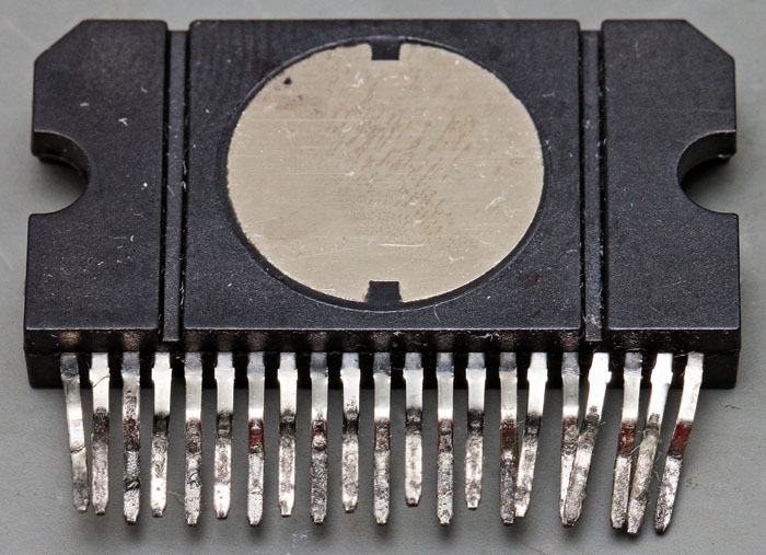
Well that´s not a big heatspreader...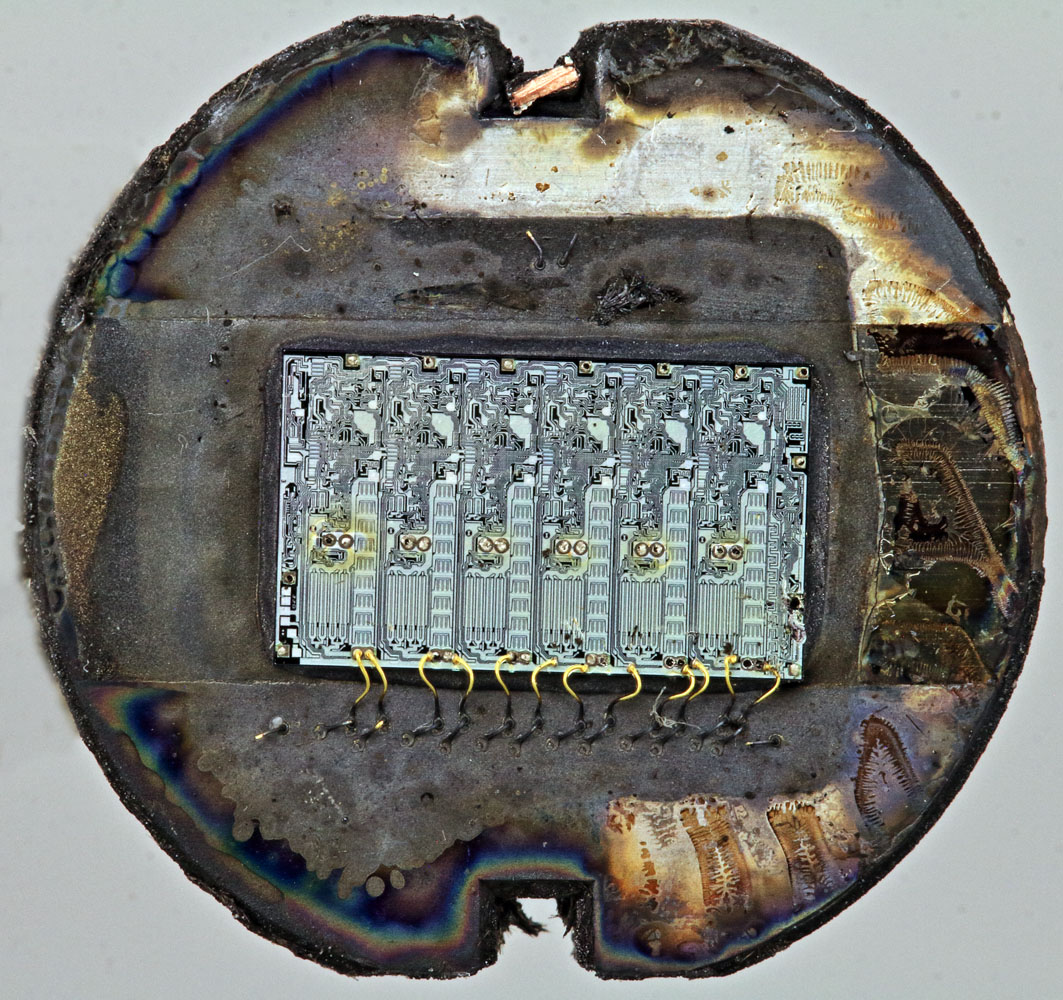
But the die is quite big: 7,2mm x 4,3mm. There are a lot of bondwires connecting the die to the heatspreader.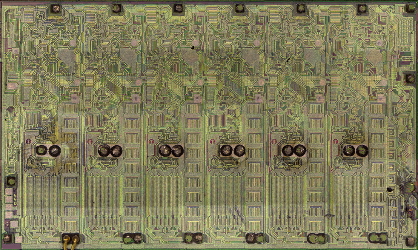
You can see the six power stages. There are six bondpads on top of the die controlling the power stages. In the middle of the die there are six times two bondpads connecting the output pin. On the lower edge there are six times two bondpads connecting to ground.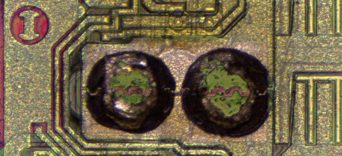
Now that´s interesting! There is a cut in the middle of the two bondpads! Perhaps Bosch wanted to use the power stage with less outputs too. I assume by not connecting the bondpad of an unused amplifier a circuit is cut open. Perhaps that was neccessary because of diagnostics...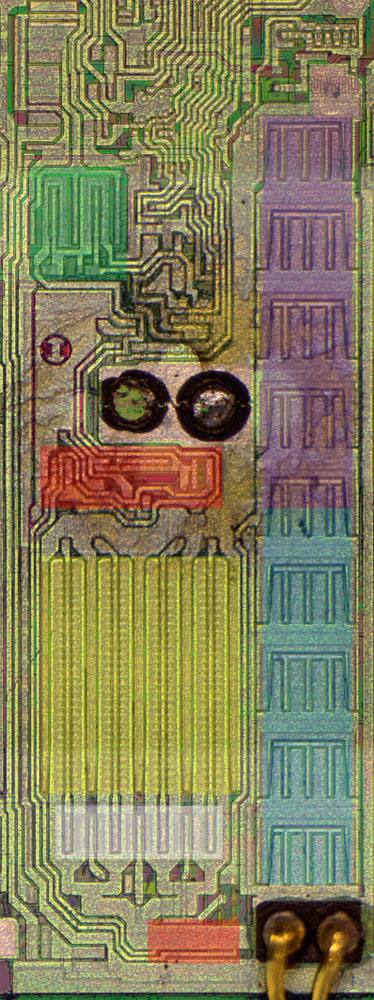
You can spot the power transistor (yellow), the overcurrent protection (red) using a part of the metal layer as a shunt, the driver (green) and a big structure (blue/purple) containing zener diodes for clamping.
Interesting is the white part. The potential between the blue and the purple part is used to control the white part.
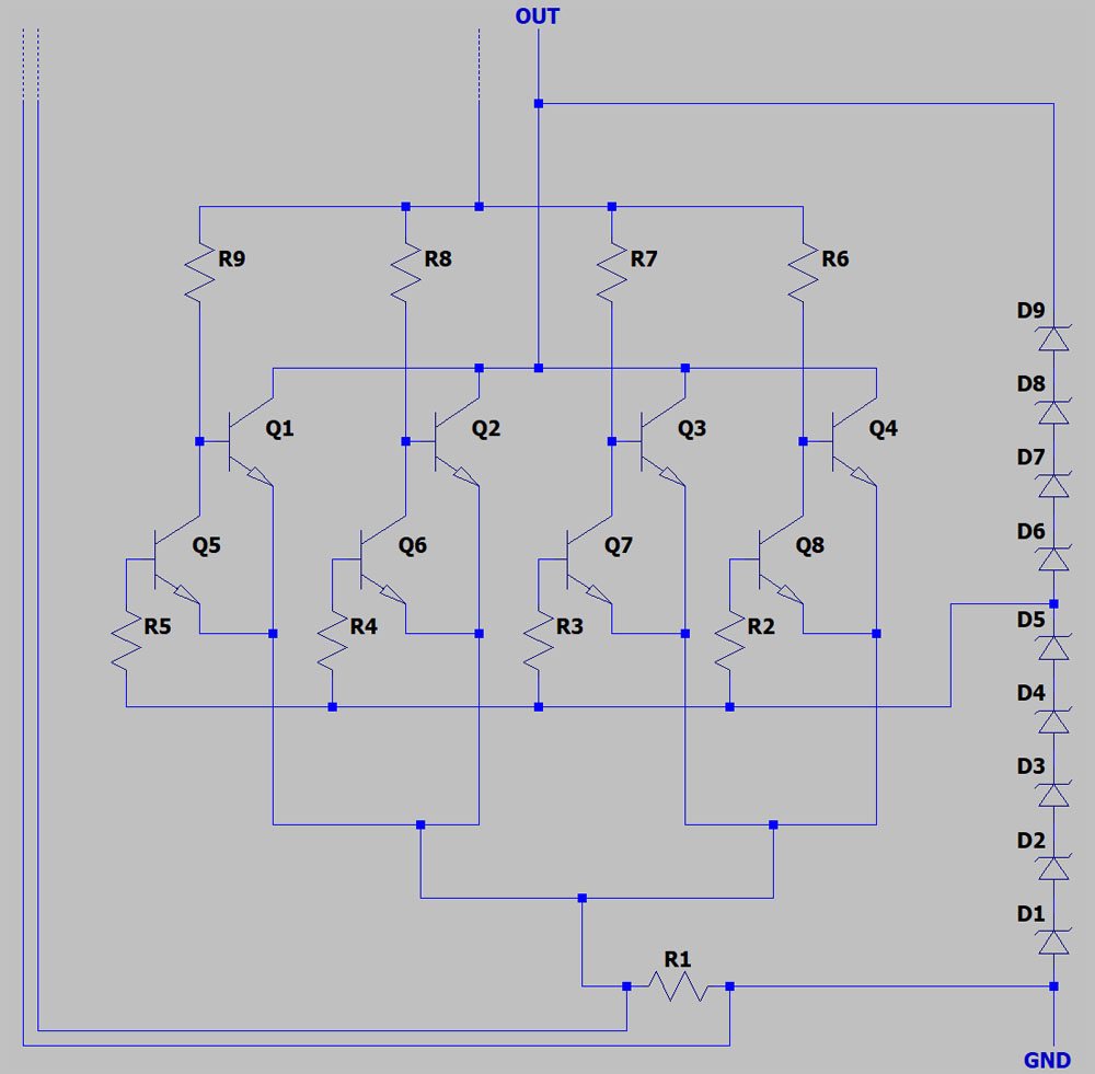
It looks like the white transistors are pulling the base of the power transistor hard low while the zener diodes are clamping. I assume with this circuit the blocking voltage of the power transistor is higher while clamping. The green part looks like a highside driver. Without a push-pull driver leackage current through the collector-base-junction can turn the transistor on. Pulling the base low drains the leackage current and gives you some more volts of blocking voltage.
https://www.richis-lab.de/ECU04.htm
-
Yeah, clamped B-E gives you the higher Vcbo versus Vceo voltage rating.
That pullup must be pretty beefy then. Not actually Darlington?
I find the layout unusual, or I'm rather rusty on reading ICs; hard to tell what's collector and emitter. And hard to see the diffusions under the metal layer; they're only barely visible in the tilted (perspective? and look at that metal thickness, cool) view.
Tim -
Another great one, thank you!
-
That pullup must be pretty beefy then. Not actually Darlington?
No, i didn´t find a darlington.I find the layout unusual, or I'm rather rusty on reading ICs; hard to tell what's collector and emitter. And hard to see the diffusions under the metal layer; they're only barely visible in the tilted (perspective? and look at that metal thickness, cool) view.
You are right. It took me some time but now I´m pretty sure about the schematic. In the white block you can see the greenish base area and looking very carefully you can spot a second area in the base area under the ground metal. That has to be the emitter. The base of the power transistor connects to the purpel area in which the greenish base area is placed. That has to be the collector. Another great one, thank you!
Thanks!
-
How are those clamping diodes supposed to work? They look like normal transistors with open circuit bases.