Hello,
I initially had a 2nd LT1037 on the output stage.
The result was massive oscillations.
(The reason for the LT1012 in the second stage).
So obviously you will have to do some additional
shielding between stages with 2 * LT1037.
with best regards
Andreas
Anyone seen these before? I bought a couple just to test out and alter a little. Some of the parts look ok and some could use replacing but you don't see completed boards very often even if missing the LTZ.
Bill
You are all really terrible.... I could not resist and I also took a couple

If it can be useful to someone, in the attachment, there is the schematic that the seller has used.
Noopy provided links to his microscopic views of the LTZ1000 chip here -
https://www.richis-lab.de/REF03.htmIn one of the images you could see light coming from the circular Zener junction. That’s very cool. So, I had to explore that.
I made a little pcb with a tall socket for the LTZ1000. It also had selectable bias currents and operating temperature.
My friend Jim has a great collection of top-of-the-line microscopes. He coupled his new Nikon Z6 to the Nikon Metaphot Metallurgical microscope for the following images.
Thanks Jim!
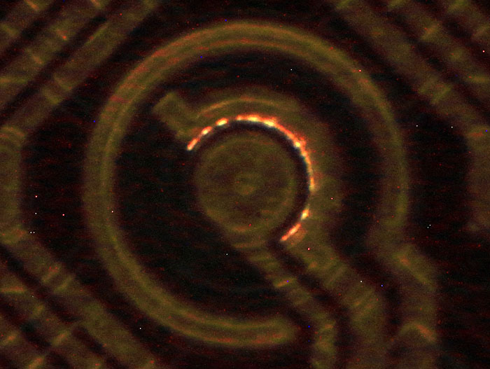
As you would expect, as the current increased the light increased.
Changing the chip temperature from 50 deg C to 95 deg C at 4ma bias made no noticeable change in the light.
For one image Jim minimized all ambient light so we could capture the full 360 circle of light from the breakdown. Half of the light is hidden behind the trace on the top layer.
Interesting how the light appears in "dots" like stars in a nebula.
Guess this is due to imperfections, so some parts of the junction breaks down more than others?
You can imagine how such a process could be electrically noisy...
It would be awesome to record that light with some kind of photodetector and "listen" to it - is the light output noisy like the zener current?
Also, what might prove interesting is to hit the junction with a LASER-- and watch what happens with the 1/f noise and voltage output. I've been wanting to do this for a long time, but it seems @chuckb beat me to it, and is pretty much ready to do this test!
Interesting how the light appears in "dots" like stars in a nebula.
Guess this is due to imperfections, so some parts of the junction breaks down more than others?
You can imagine how such a process could be electrically noisy...
It would be awesome to record that light with some kind of photodetector and "listen" to it - is the light output noisy like the zener current?
I can also imagine the light may show some fluctuations. Changes are these may correlate with noise in the voltage.
I don't think this is a kind of junction break-down. The more likely mechanism is that the zener diode in the avalanche regime produces hot electrons and some of these can get to the surface oxide / interface. Relaxation of the electrons there can happen with light at some suitable states (similar to color centers).
Normally the idea behind the buried zener is to avoid this effect by keeping the hot electron from reaching the surface. The second point is that they do less harm in the burried zener: this part can still work but is not so visible.
If the mechanism is due to electrons relaxing and "going back to bed", perhaps taking a spectrum of the light would show something interesting? (confirming the material, perhaps, and thereby proving the hypothesis?)
Interesting how the light appears in "dots" like stars in a nebula.
Guess this is due to imperfections, so some parts of the junction breaks down more than others?
You can imagine how such a process could be electrically noisy...
It would be awesome to record that light with some kind of photodetector and "listen" to it - is the light output noisy like the zener current?
I can also imagine the light may show some fluctuations. Changes are these may correlate with noise in the voltage.
I don't think this is a kind of junction break-down. The more likely mechanism is that the zener diode in the avalanche regime produces hot electrons and some of these can get to the surface oxide / interface. Relaxation of the electrons there can happen with light at some suitable states (similar to color centers).
Normally the idea behind the buried zener is to avoid this effect by keeping the hot electron from reaching the surface. The second point is that they do less harm in the burried zener: this part can still work but is not so visible.
Are you sure?
I´m no expert regarding semiconductor physics but in my understanding z-diodes with this voltage rating work at least to some extend in avalanche breakdown.
In avalanche breakdown accelerated electrons hit other electrons setting them free on a not exactly defined energy level. If the energy level is in the range of visible light their recombination can emit visible light.
This recombination will perfectly happen in the junction area. In my view most of the recombination will happen there.
Correct me if I´m wrong.
A agree one the way the zener is supposed to work. However I doubt that one would see light from the buried junction. This would be rather deep inside the silicon so only very little of that light can escape. The normal avalanche process should also not produce light as the energy from the hot electron is used to generate new pairs. The normal recombination in silicon is without any light and if any it would be in the IR range (~ 1 µm). It would be only if a hot electron recombines or excites some defect in some way.
It usually takes some defects so that an indirect semiconductor like silicon can emit light. The logical position would be the surface or just inside the oxide. My estimate is that the way to the surface should be easier for a hot electron than for visible light. This would be different if the light is in the NIR range.
However I doubt that one would see light from the buried junction. This would be rather deep inside the silicon so only very little of that light can escape.
I´m not sure about this.
A view days ago I tried to use a big KD501 transistor as a photovoltaic cell.
(
https://richis-lab.de/Bipolar02.htm)
Across the base-emitter-junction I got the same current as across the base-collector-junction. It seems there wasn´t significant light reduction.
The normal avalanche process should also not produce light as the energy from the hot electron is used to generate new pairs. The normal recombination in silicon is without any light and if any it would be in the IR range (~ 1 µm). It would be only if a hot electron recombines or excites some defect in some way.
I agree with you that hot electrons generate new pairs but some of them will recombinate. Otherwise you will get a real breakdown with 0V and destruction of the junction. (I´m not absolutely sure about the last sentence but that would be my interpretation.)
The hot electrons can have a higher energy than you will see while normal current flow in the semiconductor. With "normal" current flow and "normal" recombination you don´t see any light. I agree with that. But in my view there is recombination of hot electrons.
I tried to take a "maximum tilted" picture but you can´t really say where the light is generated:
How deeply is a buried zener buried? May be the layer above it is thin-enough to be transparrent to the light? May be photons from inner layer somehow re-emmiter from the outer layer? (purelly guessing here, I have zero knowledge about semiconductors)
However I doubt that one would see light from the buried junction. This would be rather deep inside the silicon so only very little of that light can escape.
I´m not sure about this.
A view days ago I tried to use a big KD501 transistor as a photovoltaic cell.
(https://richis-lab.de/Bipolar02.htm)
Across the base-emitter-junction I got the same current as across the base-collector-junction. It seems there wasn´t significant light reduction.
The normal avalanche process should also not produce light as the energy from the hot electron is used to generate new pairs. The normal recombination in silicon is without any light and if any it would be in the IR range (~ 1 µm). It would be only if a hot electron recombines or excites some defect in some way.
I agree with you that hot electrons generate new pairs but some of them will recombinate. Otherwise you will get a real breakdown with 0V and destruction of the junction. (I´m not absolutely sure about the last sentence but that would be my interpretation.)
The hot electrons can have a higher energy than you will see while normal current flow in the semiconductor. With "normal" current flow and "normal" recombination you don´t see any light. I agree with that. But in my view there is recombination of hot electrons.
I tried to take a "maximum tilted" picture but you can´t really say where the light is generated:
Several things to note here:
1) If the emission is happening underneath an oxide layer, let us remember that we call the silicon dioxide we encounter on an everyday basis "glass". No problems with light getting through centimetres of glass, let alone microns or 100s of nanometers.
2) The assumption made so far is that silicon is the emission candidate. What if it's the dopant? Several common dopants are very strongly associated with visible emission bands (common: arsenic, phosphorous, less common: gallium). There is, admittedly, very little dopant but we're seeing very little light.
3) The assumption that the material is "too thick" for emissions to make their way out. Remember that we are in the 100s - 1000s of nanometres territory here. At that scale one's assumptions brought from the normal scale world about opacity are quite likely to be wrong.
This diagram of the structure of the buried Zener from the LM399 might be instructive at this stage. It looks to me like the emission is happening well away from the region where the 'buried' junction action is supposed to be going on, perhaps between the outer ring of P- diffusion and the N- substrate or between the cathode and the surface part of the anode P- diffusion.

...
Several things to note here:
1) If the emission is happening underneath an oxide layer, let us remember that we call the silicon dioxide we encounter on an everyday basis "glass". No problems with light getting through centimetres of glass, let alone microns or 100s of nanometers.
2) The assumption made so far is that silicon is the emission candidate. What if it's the dopant? Several common dopants are very strongly associated with visible emission bands (common: arsenic, phosphorous, less common: gallium). There is, admittedly, very little dopant but we're seeing very little light.
3) The assumption that the material is "too thick" for emissions to make their way out. Remember that we are in the 100s - 1000s of nanometres territory here. At that scale one's assumptions brought from the normal scale world about opacity are quite likely to be wrong.
This diagram of the structure of the buried Zener from the LM399 might be instructive at this stage. It looks to me like the emission is happening well away from the region where the 'buried' junction action is supposed to be going on, perhaps between the outer ring of P- diffusion and the N- substrate or between the cathode and the surface part of the anode P- diffusion.
(Attachment Link)
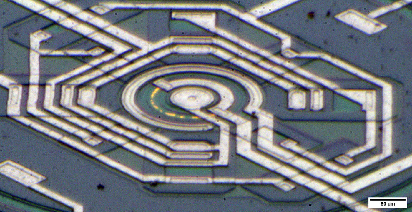
I agree with you in most points except the last one. Be aware that the round thing in the middle of the LTZ1000 is a buried zener
and a transistor.
I took also a picture of the transistor working in breakdown:
=> The z-diode has to be around the transistor.
I agree with you in most points except the last one. Be aware that the round thing in the middle of the LTZ1000 is a buried zener and a transistor.
I took also a picture of the traor working in breakdown:
=> The z-diode has to be around the transistor.
Even with my very limited understanding of silicon fabrication I don't believe that is right. The circular structure fits every diagram of a buried zener that I've ever seen, and the structures further out (outside the central region) look much more like what I understand a bipolar transistor to look like on a die. There are more than the two shown in the schematic (I can see 4 things that definitely look like transistors, perhaps even eight), but it is quite common for multiple transistors to be paralleled 'on chip' into a single transistor to allow for thermal balancing, dealing with thermal gradients and the like - exactly what one might expect on a chip like the LTZ1000.
I'd be deeply grateful if someone who is actually properly qualified at decoding dies shots would produce an annotated version of one of the many LTZ1000 die shots kicking about marking out the actual transistors, their CBE connections and so on.
Can you buy 'reasonably priced' germanium microscope optics to allow an IR camera to be used to show where currents flow and the current densities?
Even with my very limited understanding of silicon fabrication I don't believe that is right. The circular structure fits every diagram of a buried zener that I've ever seen, and the structures further out (outside the central region) look much more like what I understand a bipolar transistor to look like on a die. There are more than the two shown in the schematic (I can see 4 things that definitely look like transistors, perhaps even eight), but it is quite common for multiple transistors to be paralleled 'on chip' into a single transistor to allow for thermal balancing, dealing with thermal gradients and the like - exactly what one might expect on a chip like the LTZ1000.
I'd be deeply grateful if someone who is actually properly qualified at decoding dies shots would produce an annotated version of one of the many LTZ1000 die shots kicking about marking out the actual transistors, their CBE connections and so on.
Well looking in detail at my own assumptions I have to admit you are right. But I´m right, too.

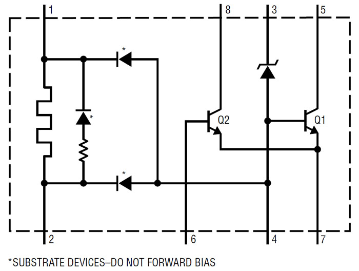
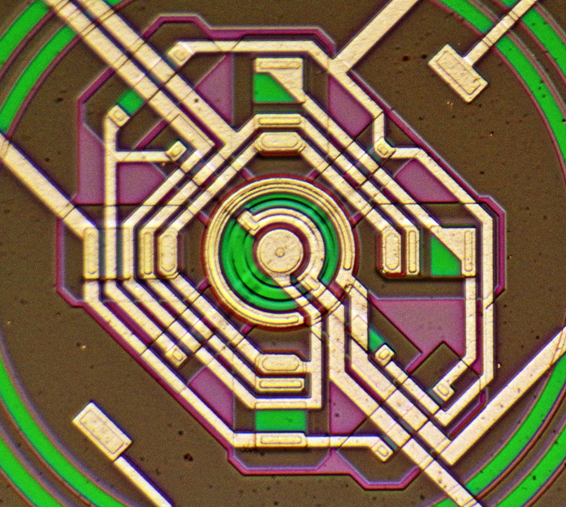
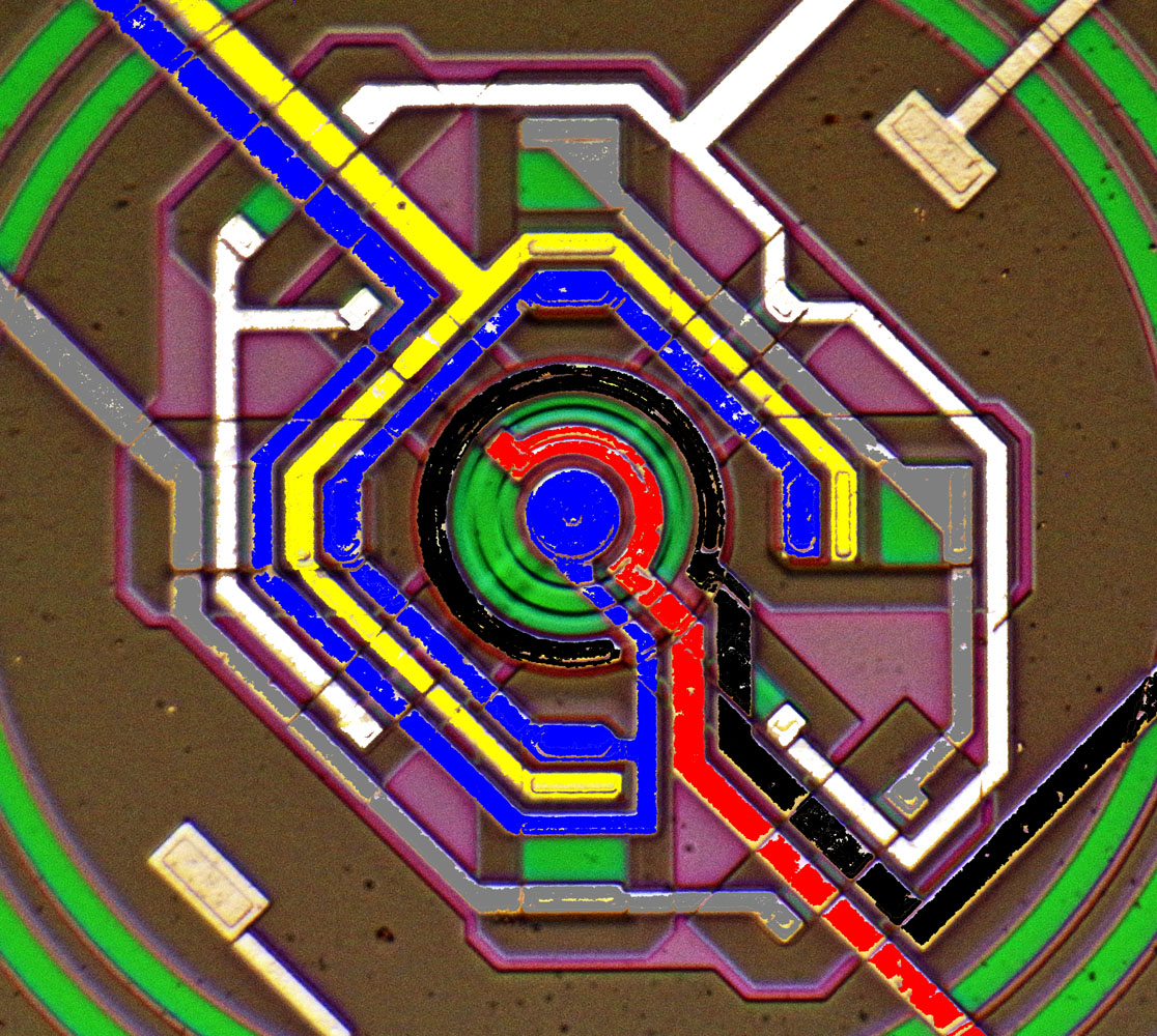
The z-diode is designed as descriped in the LM399 diagram. It is connected with the red metal (cathode) and the black metal (anode).
The transistor Q1 is already there with it´s emitter connected to the blue metal in the center. The base is a part of the z-diode (red). The collector is connected from the edge (white).
So there is a transistor which is surrounded by the z-diode but it´s already in the z-diode structure.
The "avalanche lights" confirm this: You can see the base-emitter-junction on the edge of the middle circle whereas the z-diode-junction is buried under the surrounding ring.
Q2 consists of four transistors surrounding the z-diode and Q1 (grey, yellow, blue).

Can you buy 'reasonably priced' germanium microscope optics to allow an IR camera to be used to show where currents flow and the current densities?
I´m afraid such an optic is unaffordable...


