When i'm generally need 2 of these boxes for DC.
Why is Tekbox selling them as single?
If i need 2 it is only that i need the inductors also in GND path or?
So i can also tweak the PCB to have additional inductors in GND or? Which GND for Attentuator / SMA then? DUT or Supply side?
When i'm generally need 2 of these boxes for DC.
Why is Tekbox selling them as single?
If i need 2 it is only that i need the inductors also in GND path or?
So i can also tweak the PCB to have additional inductors in GND or? Which GND for Attentuator / SMA then? DUT or Supply side?
Hi,
If you know that the conducted emissions are differential mode noise, then you can use one LISN for pre-compliance testing.
Most of time with small power supplies the conducted emissions are dominated by DM mode noise so this is justified.
If you use one LISN the DM mode signal twice a big, 6dB, higher than if you use two LISNs. This is because half the DM signal will appear on one LISN and the other half on the other LISN.
The difference between 50

and 100
for one versus two LISNs normally isn't important because the emission source impedance is usually very low.
You can build a double LISN like this:


(This is a LISN designed for CISPR 32)
(A shoutout for the ZofzPCB Gerber viewer -
www.zofzpcb.com)
If you use two LISNs you can use a DM/CM Separator to determine if the emissions are CM or DM.
I described the construction of one of these in this thread:
Link:
https://www.eevblog.com/forum/projects/diy-dm-cm-seperator-for-emc-lisn-mate/msg3117396/#msg3117396Regards,
Jay_Diddy_B
When i'm generally need 2 of these boxes for DC.
Why is Tekbox selling them as single?
If i need 2 it is only that i need the inductors also in GND path or?
So i can also tweak the PCB to have additional inductors in GND or? Which GND for Attentuator / SMA then? DUT or Supply side?
If you use one LISN the DM mode signal twice a big, 6dB, higher than if you use two LISNs. This is because half the DM signal will appear on one LISN and the other half on the other LISN.
The difference between 50 and 100 for one versus two LISNs normally isn't important because the emission source impedance is usually very low.
True, true. If we model the source impedance as...1 ohm, then the difference in EMI levels will be around 1%, with a single LISN (50 ohm DM impedance) vs. dual LISN (100 ohm DM impedance). The 1 ohm number is just a guess though. But just to clarify, mostly for Noy, even though the loading effects of single vs dual LISN are not (usually) significant, with a single LISN, the detected level will be twice as high for the reason you mentioned. If going the single LISN route, maybe he/she can put a 6dB attenuator between the LISN and spectrum analyzer/receiver, or tell your EMI software to drop the detected level by 6dB.
All that said, in my limited experience, CM noise is usually
not insignificant. But, that's limited to a certain variety of power supplies. If you don't have a good feeling about whether your DUT will produce significant CM noise, then my recommendation is to use two LISNs. At low power, the BOM difference is not significant. For high current LISNs, the BOM cost may be more significant.
Generally there isn't much common mode from a device that only has two terminals (i.e., the power cable and no other connections), but it can still appear, as the device itself has capacitance to free space, thus there is a return path for CM at high frequencies.
If there are additional connections, then not only can there be unbalanced currents among them (and therefore CM back to the LISN), but external connections should be terminated in a similar way, e.g. telecom pairs through a CDN (see for example CISPR 22).
There aren't many applications for a single terminal device, but it might happen in automotive components for example, where one power wire goes out, and return currents flow through the chassis -- in the lab, the ground plane. This would only need one LISN port, by definition (there's no point in connecting a port to the reference plane, it's defined as zero).
Generally, short or permanent connections between components of the EUT should be laid out in a representative fashion. Maybe they'll act as stubs and affect the EMI profile of the EUT, who knows; hence, "representative". Some standards do perform measurements on such cabling, adding loading ferrites to trim the impedance, using current clamps and inductive or capacitive couplers to read emissions or inject noise...
The assumption underlying all of this, is that the system can be analyzed as a network between a number of ports. The LISN is an interface, joining an endpoint of the EUT's network, to a source, which might be passive (a termination resistor say), or a transmitter or receiver. The response across multiple ports may or may not be relevant (NM on wire(s); CM/DM on wires in a cable; between cables; etc.). The point is, everything required is available on ports, so that whatever the desired analysis is, it can be performed (e.g., using a CM/DM splitter transformer).
Tim
I changed some things at the schematic.
But I'm unsure about the correct cap values on the supply side. Which one do i need and which value is needed?
Is it important for EMI precompliance to know if its CM/DM is? I cant remind that in the laboratory there where different CM/DM measurments. Only if the emission is to high or not. Normally i have to measure for EN55011 or EN55022 where can i find my needed L/C values for these kind ?
The scanned EMI level is the composite (addition) of CM and DM noise. The standards do not put limits on CM or DM individually, but both contribute to the EMI profile of the DUT. If you only use on LISN, potentially you will have inaccurate/misleading results, if your DUT produces excess CM noise, since you will not detect it. If you do not know the nature of your DUT (whether or not it produces significant CM noise), it's best to test with two LISNs.
Currently I'm unsure if i need the 5uH or 50uH "version".
For EN55011 or EN55022 it looks like 50uH is defined?
So can i simply change the Inductors to one of these? Most times <=5A would be enough for my devices:
74439358100
74439370100
74439346100
Biggest one 74439346100 is 10uH and can provide 10A. But i don't know if i have to watch for something special about the inductors. SRF for example?
Who knows and give me an advice?
Hi,
Both EN55011 and EN55022 are mains voltage requirements.
The 5uH LISN described in this thread is only suitable for low voltage applications (automotive).
For mains voltage you need something like the TekBox TBLC08.
Jay_Diddy_B
OK it looks like EMI laboratory simply use the EN55011 / EN55022 LISNs (CISPR11 / CISPR22) also for our DC devices.
So i will need a 50uH version with >=5A <=60V.
I think i will use the shown schematic and change some values. For the inductors i will use 7443331000 ones. These are enough for >= 5A and <60V.
And SFR with 35MHz should work or? I must measure 150kHz up to 30 MHz.
I found something that there are 250uH inductors in the AC ones. But these are for AC filtering only or? So i can build it without. I only need 50uH and 5Ohm with sufficient caps?
The CM/DM circuit is flawed you said. But how big will the "failure" be? Is it good enough for indication if CM or DM is the bigger part? I ask because its easier to put this additionaly on the pcb vs. the coupled inductor part especially if this transformer is not the easiest thingy and "pretty big".?
SFR can be somewhat below 30MHz even, as long as it is the parallel resonance (maximum Z == least attenuation of signal). The hazard is the first series resonance, or whatever the impedance is doing up there.
Inductors with certain distributions of losses, can work just fine well past there, as long as you don't mind that the impedance is real, that it's sufficient for it to be high enough (e.g., >500 ohms for a < 1dB error on a 50 ohm system). This is the general plan behind stacking inductors, particularly in a geometric series, and often with added lumped losses (resistors or RC or RL networks) to control the series resonances between adjacent inductors.
Mind that the inductors need to not saturate at whatever peak current you're using them at; otherwise those peaks will be attenuated at low frequencies.
Tim
Thx for clarification.
So i have started again i found this (see attachment).
But I'm unsure if i need this 250uH thing at the input. My guess was i will simply use the 5uH LISN approach here uwith other values.
5x 7443331000
And other 2x 4uF caps at the supply side in series with some resistors (maybe 4x 1206 parallel for the 5 Ohms) or so.
And the stuff going to the spectrum analyzer nearly the same except the first resistors -> should be 1k .
But my DC lab Supply has output caps so i think i need something in there that the 5Ohm resistors are used. But 250uH for 5A is pretty big..
So anny suggestions? Maybe anoterh 1-2 x 7443331000 towards the DC Supply are enough?
Hi Noy,
The Wurth 7443331000 is a good choice for the inductor.
I use 4x 2.2uF capacitors in parallel to make the 8uF
I use 2x 10
resistors in parallel to make the 5
resistor.
This is the schematic:


You need two copies of this schematic.
Build the circuit like this:


The 1k
in your schematic is a safety resistor it keep the output of the LISN near ground if the LISN is not connected to a 50
load (Spectrum Analyzer).
My schematic includes a 9kHz HP filter, which is also a dc block, and a 10dB attenuator. These are to protect the spectrum analyzer.
Do not change the 'first' resistor to 1k
.
This will result in a low voltage LISN suitable for around 5A and <50V.
The 250uH inductor in your schematic works as a line filter. It keeps noise from the input appearing on the LISN output. If you feed the input with a clean bench power supply, not a switching supply, you do not need this filter.
Regards,
Jay_Diddy_B
Hi Noy and the group,
I have looked at the PCXB design proposed by Noy. The copper area on the connections to the device under test should be reduced:


They should be reduced to the minimum that is required to handle the current, like this:


This is done to reduce the capacitance to the ground plane. If you don't do this, there will be a resonance at around 30-40 MHz.
Transient LimiterThis LISN has the transient limiter built in. There is no benefit to adding a second transient limiter. It will reduce the signal amplitude by an additional 10dB.
This transient limiter is based on the HP 11947A and will provide adequate protection.
There is no benefit to adding a PIN diode limiter in parallel with the inductor. It will not work, the PIN diode limiter has to be capacitor coupled.
Regards,
Jay_Diddy_B
Thx for your advice.
Corrected it.
For all who are interested, please find attached die Kicad Project.
Edit: Updated Projekt Files (Silkscreen, recalculated trace with for CPWG), added Gerbers, BOM, Schematic PDF
Edit2: JLCPCB charges 4$ engineering fee but i don't know why.. gerbers are looking fine..
Edit3: Found out why.. PCB is taller than 102x102mm...
Edit4: Updated Silkscreen for µH / Version Marking
Edit5: Corrected pcb edge radius to r=5mm
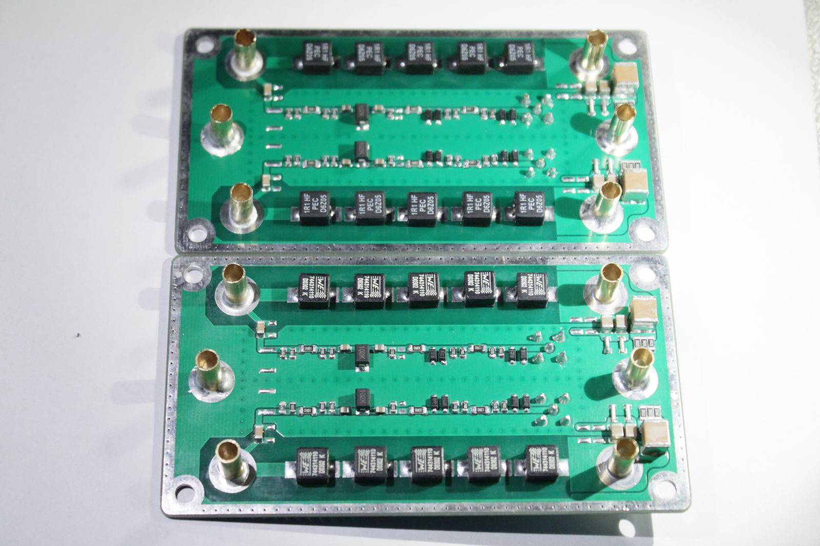
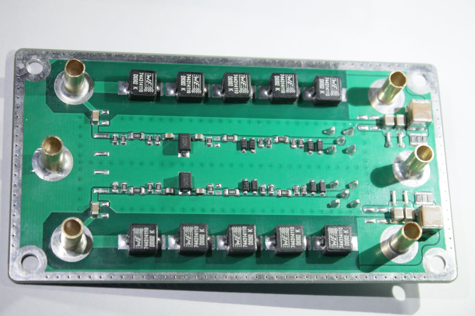
Many thanks to Jay_Diddy_B and Noy who decided to share his PCB project.
Below photos of assembled dual 5uH LISN. This is
previous revision of Gerber files with corner radius slightly too small.
I made two units with different inductor types to see the difference.
A minor change in Noy's design is using Jay_Diddy_B's resistors values in attenuation section.
One comment is that soldering to footprints without thermal reliefs is difficult and in my case pushed me to use SnPb solder.

Just sent into production a LISN PCB built using the schematics that @Jay_Diddy_B sent me  . I arranged it so that it goes directly into the Bud industries EX-4521 enclosure. The front and rear panel are also PCBs, something I have long wanted to make
  .
.
Hi prasimix,
Can you share more info for your project?
Have you assembled it?
Did it work?
Can you post schematics and/or gerbers?
Thanks
Thanks Noy, great project!
Am I right when calculating the thickness of your LISN-PCB to 0,7mm? This is because at least the 1,231mm trace to the SMA-connector should have an impedance of 50 Ohms.
This is calculated with FR-4 to 49,35Ohms for this 1,231mm trace, then.
Please correct me if I'm wrong!
For the CM/DM-Seperator I found a trace of 1,65mm width that is calculated to 51,5Ohms with a PCB-thickness of 1mm?
Thanks again as always also to Jay Diddi!
No 1.6mm jlcpcb: With 1.53mm fr4, 0.035mm cu and er of 4.5 for fr4 and gap of 0.2mm .
But not microstrip! Coplanar wave guide with ground.
Okay,
thank you Noy!
That is very welcome information as calculator for coplanar waveguide with ground is very rare to find a tool for...
I didn't found it on easyeda or jclpcb but ordered there, too.
In AD19.1.7 this calculator is missing. It was added later in AD20 and tuned up to AD21.
Which PCB-tool did you use for this calculation?
Please, can you calculate the thickness of Jay_Diddy_Bs DIY DM/CM Seperator design?
(
https://www.eevblog.com/forum/projects/diy-dm-cm-seperator-for-emc-lisn-mate/msg3117396/#msg3117396)
The Trace width is 1.65mm and the gap is 0.28mm there.
Seems that it needs a different PCB thickness then...