Author Topic: Opamps - Die pictures  (Read 277296 times)

0 Members and 19 Guests are viewing this topic.

Online magic

  • Super Contributor
  • ***
  • Posts: 8062
  • Country: pl
Re: Opamps - Die pictures
« Reply #250 on: March 27, 2022, 06:56:43 pm »
Cascoding of current sources makes sense as it should improve output impedance and bandwidth; LF156 did it too.

The second stage is less obvious, because NPNs could be used here in theory and those JFETs take more space than OP07 or OP27 input pair. What isn't clear is whether an ordinary NPN differential pair would permit a three stage topology in some manner - common three stage opamps from the era used PNP second stage which naturally feeds an ordinary NPN VAS, while OPA111 employs that weird arrangement with common base NPNs driven by JFETs which likely couldn't be replaced by PNPs.

OPA111 appears to benefit from its three stage architecture with high guaranteed gain (120dB) and CMR/PSR better than two stage designs like TL072 or LF156, including BB's improved derivatives such as OPA156, OPA2107, OPA606.


Regarding noise, this was said in the datasheet:
Quote
Extremely low noise is achieved with patented circuit design techniques. A new cascode design allows high precision input specifications and reduced susceptibility to flicker noise.
and AD's applications handbook by Jung:
Quote
The OPA111 circuit employed P-channel JFETs in the input and second stages, and a first stage cascode design for low bias current variation with input CM changes. The design addressed some of the weak points of the previous LF155/156/157 series (Reference 39, again). Reference 49 cited several LF15x circuit weaknesses; one was the use of current source loading for the input JFET pair, another was the means of offset trimming, and another was potential susceptibility to popcorn noise, due to the noise currents of the second stage bipolar differential pair. These points were addressed by the OPA111 design.

Reference 49 is Steve Millaway, "Monolithic Op Amp Hits Trio of Lows," Electronic Design, February 9, 1984, which I wasn't able to locate even after signing up to ED's website.
 

Offline NoopyTopic starter

  • Super Contributor
  • ***
  • Posts: 2401
  • Country: de
    • Richis-Lab
Re: Opamps - Die pictures
« Reply #251 on: April 03, 2022, 03:39:47 am »


Another µA709 variant, a TL1709 built by Telefunken. The TL1709C is the consumer part.


The datasheet looks familiar.


The design of the die looks familiar too but it seems to be a proprietary development.


The test transistor is strange... What are the purple areas doing?  :-//


https://www.richis-lab.de/Opamp47.htm

 :-/O


I somehow lost track of the circuit. Let´s fetch the schematic of the LM709 because there are designators:


What was the job of Q7?  :-//
@magic?  ;)
 
The following users thanked this post: SeanB, RoGeorge, magic

Offline T3sl4co1l

  • Super Contributor
  • ***
  • Posts: 22435
  • Country: us
  • Expert, Analog Electronics, PCB Layout, EMC
    • Seven Transistor Labs
Re: Opamps - Die pictures
« Reply #252 on: April 03, 2022, 04:44:45 am »
Is that kinda like a Vbe multiplier, between Q8/Q9 bases?  Looks weird because it just happens to also be the diff pair biasing?

Next thought: Q15 and Q4/Q6 act like a current mirror, balancing the current in R1/R2 with R5/R6... making sort of a current source or something?

It's also tied in with main bias (~Q10), which isn't going to be very stable, but varies with signal level.  Or maybe that's been balanced too.

These old, highly optimized (tightly coupled) ICs are always something of a puzzle to tease out. :)

Tim
Seven Transistor Labs, LLC
Electronic design, from concept to prototype.
Bringing a project to life?  Send me a message!
 
The following users thanked this post: Noopy

Online magic

  • Super Contributor
  • ***
  • Posts: 8062
  • Country: pl
Re: Opamps - Die pictures
« Reply #253 on: April 03, 2022, 09:01:01 am »
This Telefunken schematic is hundred times more logical than Widlar's mess.

OK, let's go. We apply power, all transistors are off, the 10kΩ start to conduct. Second stage output emitter followers turn on, the left one pulls up input stage collector loads. The second stage turns on and supplies power to the bias generator (approximately 3.6kΩ||10kΩ + 18kΩ), a fraction of that current is mirrored by the Widlar current source into the input pair and drops some smaller voltage across 25kΩ. This pulls down on second stage bases, stabilizing the second stage common mode level.

I suppose most of the supply voltage is dropped across the bias generator (~21kΩ), four times less is dropped across the two 10kΩ resistors (they are paralleled as far as bias is concerned) and emitter-collector voltage of the second stage is perhaps a (low) few volts, determined by three diode drops plus 25kΩ voltage (which is a certain ratio of 21kΩ voltage). All nice and stable (ignoring supply variations) and input common mode swing is entirely absorbed by input stage collectors.

3kΩ resistors and the NPN diode bias the Darlington pairs of the second stage: a small current exiting the driver through 3kΩ is enough to turn on the inner transistor much harder so it conducts most of the pair's current.

Differential voltage across 25kΩ produced by the first stage is amplified at the 10kΩ resistors by the second stage. The right side goes straight to an NPN emitter follower. The left side goes to a different NPN emitter follower which slightly shifts common mode point of the second stage and thus drives a PNP emitter follower hanging off the second stage emitters. The difference between the complementary emitter followers determines 1kΩ resistor current, which is passed to the third stage by the PNP.

Resistors in the third stage need to be calculated so as to produce the right current in 1kΩ when the second stage is in balance. Knowing Widlar, they likely are, but checking this would require calculating the input stage current source's behavior. I'm too lazy/clueless, so if I really had to do it, I would just load the circuit into SPICE. The third stage itself is a fairly simple common emitter NPN loaded with 20kΩ which drives a pair of complementary emitter followers in class B. The 30kΩ appears to implement some local negative feedback in this stage.

edit
We should perhaps consider that NPN,1kΩ,PNP,10kΩ stack to be the third stage as it works outside the second stage and VAS local compensation loops and clearly has some voltage gain of its own: 10x ignoring base impedance of the VAS, but VAS rE is 26mV/0.7mA = 37Ω so its input impedance ought to be β times more or a few kΩ. So actual gain of this stage is maybe 3~5x. Then the VAS is the fourth stage.
« Last Edit: April 03, 2022, 10:08:00 am by magic »
 
The following users thanked this post: Noopy

Offline NoopyTopic starter

  • Super Contributor
  • ***
  • Posts: 2401
  • Country: de
    • Richis-Lab
Re: Opamps - Die pictures
« Reply #254 on: April 03, 2022, 05:30:28 pm »
These old, highly optimized (tightly coupled) ICs are always something of a puzzle to tease out. :)

I totally agree with you!
These people were genius getting the most out of a few non ideal parts.  :clap:


...

Thanks!  :-+

Offline MegaVolt

  • Frequent Contributor
  • **
  • Posts: 933
  • Country: by
Re: Opamps - Die pictures
« Reply #255 on: April 04, 2022, 08:41:14 am »
What is a round area? I have seen something similar only on buried zener diodes.
 

Offline NoopyTopic starter

  • Super Contributor
  • ***
  • Posts: 2401
  • Country: de
    • Richis-Lab
Re: Opamps - Die pictures
« Reply #256 on: April 04, 2022, 08:47:44 am »
That´s a PNP transistor. Nothing too special.

Here for example in a Raytheon LM318:


Sometimes they are oval.
 
The following users thanked this post: MegaVolt

Offline NoopyTopic starter

  • Super Contributor
  • ***
  • Posts: 2401
  • Country: de
    • Richis-Lab
Re: Opamps - Die pictures
« Reply #257 on: April 13, 2022, 10:19:58 am »


LA741, one more µA741 variant. There is no manufacturer logo and I found no datasheet but with the "LA" I assume it was built by Sanyo.


Here the negative supply is connected directly to the case.


The die looks pretty similar to the RCA CA741 (https://www.richis-lab.de/Opamp45.htm).


The schematic of the CA741 applies to the LA741 too. There is just one resistor missing on the die: R13.


R4 (bias current input stage) can be changed by modifying the metal layer.

In the right part of the picture there is a small unconnected resistor. It looks like it belongs to R11 but perhaps it is an option to get  R13 into the system.


It looks like the die got a little hot at the output bondpad.  :o


https://www.richis-lab.de/Opamp48.htm

 :-/O
 
The following users thanked this post: SeanB, RoGeorge

Online magic

  • Super Contributor
  • ***
  • Posts: 8062
  • Country: pl
Re: Opamps - Die pictures
« Reply #258 on: April 13, 2022, 03:52:17 pm »
R13 was a pinch resistor on implementations that had it so the unused one seems related to R11.

This looks like a perfect copy of Fairchild. The only difference I see is lack of the "A" mark under the unused transistor at the top, but even that square/circle mark between the input pads is preserved.
 
The following users thanked this post: Noopy

Offline NoopyTopic starter

  • Super Contributor
  • ***
  • Posts: 2401
  • Country: de
    • Richis-Lab
Re: Opamps - Die pictures
« Reply #259 on: April 13, 2022, 07:04:48 pm »
You are right, in both points.  :-+

Offline NoopyTopic starter

  • Super Contributor
  • ***
  • Posts: 2401
  • Country: de
    • Richis-Lab
Re: Opamps - Die pictures
« Reply #260 on: May 13, 2022, 07:09:52 pm »


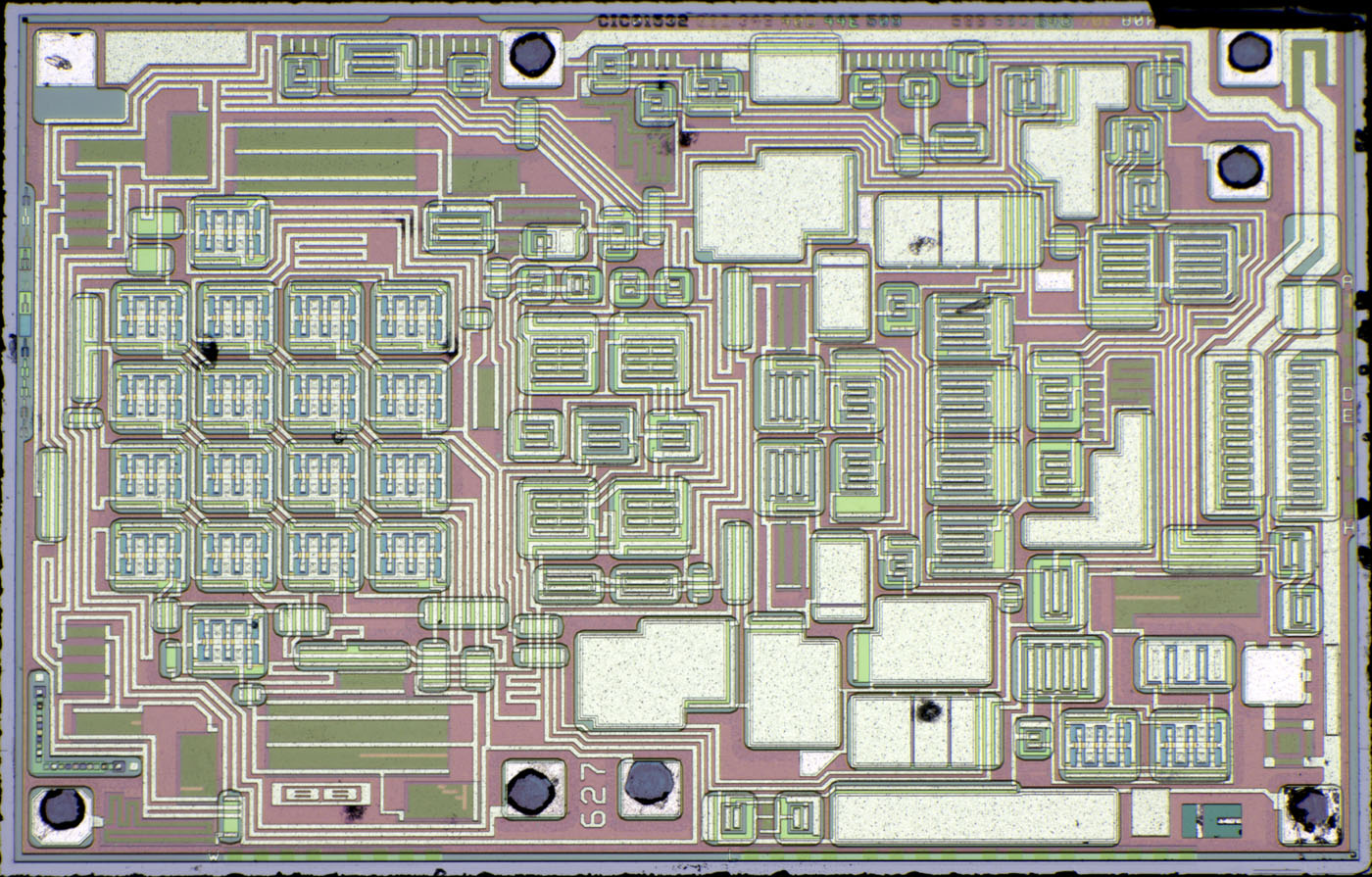
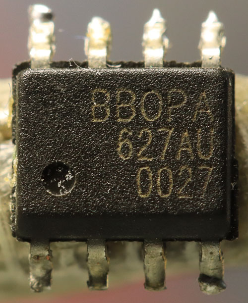
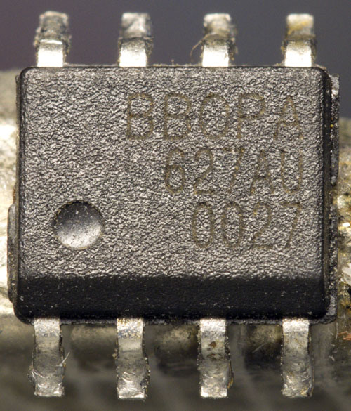
floobydust had two OPA627 which puzzled him. He thought they could be fake parts.

The markings are very hard to reed.
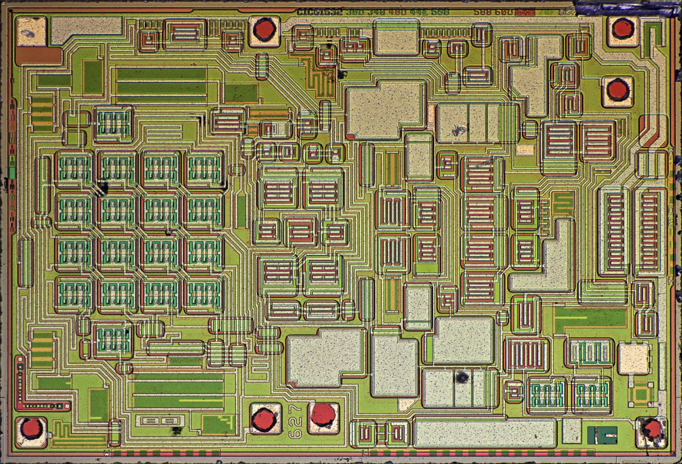


Not fake part!  :-+
Now we have better pictures of the OPA627!  8)
Of course we can´t be sure if they are recycled or scrapped parts...  :-//


Mask revisions are the same as in the "old" OPA627.
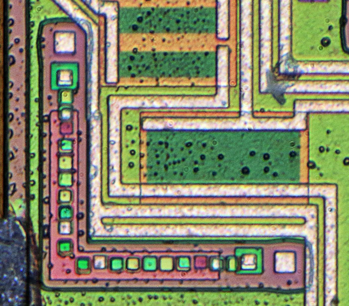


Yeah, my pictures are getting better.  8)
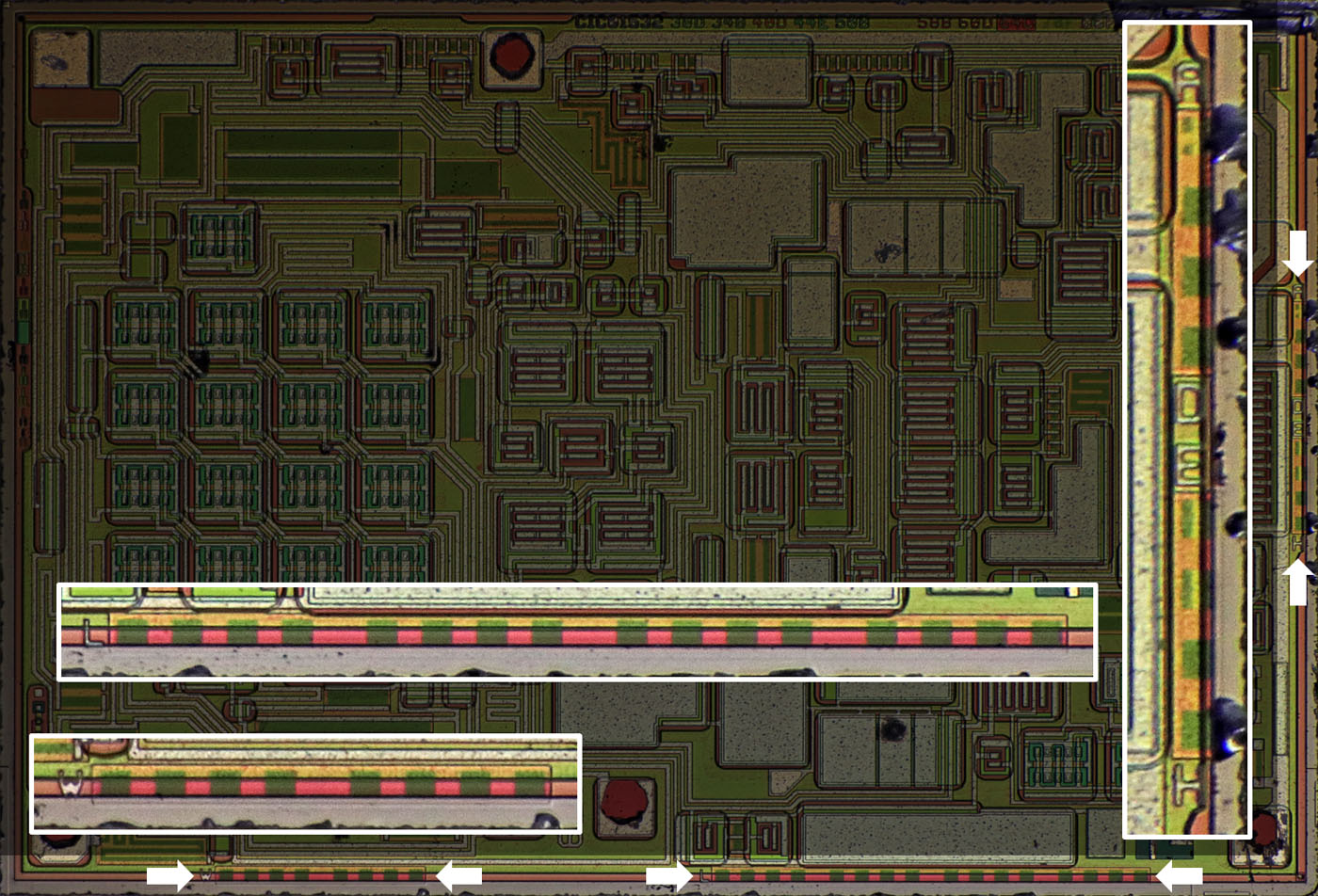


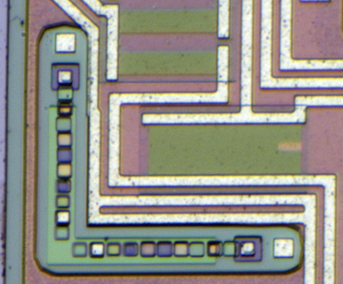
As with many other Burr-Brown parts that are laser trimmed, there are non-functional squares on the edges that have been partially cut. A letter is assigned to every square. For the ISO120 (https://www.richis-lab.de/iso01.htm) these are A to T. For the OPA541 (https://www.richis-lab.de/Opamp02.htm) and the VFC110 (https://www.richis-lab.de/vfc01.htm) A to H was enough. In the OPA627 squares from A to W were integrated.
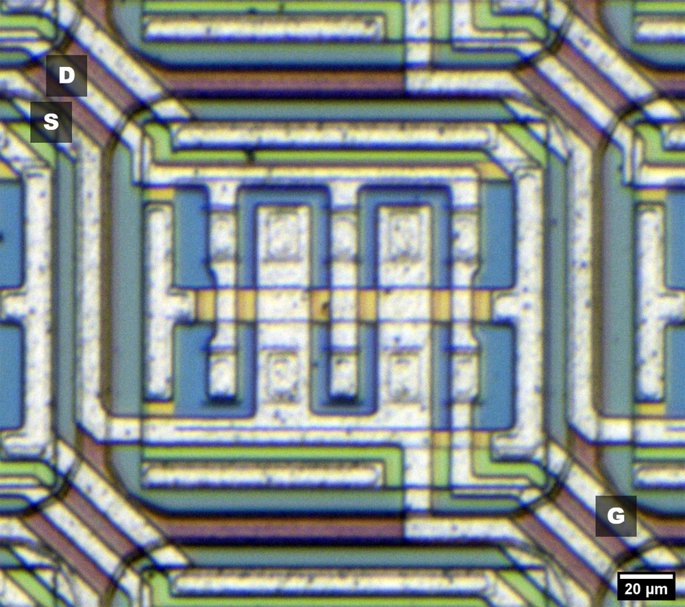


One of the p-channel J-FETs at the inputs.
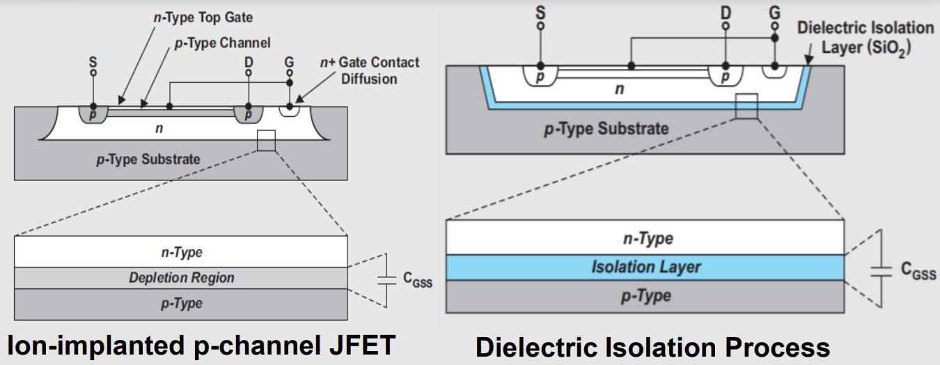


In the Analog Applications Journal (SLYT595) Texas Instruments shows what is meant by dielectric isolation. On the left you see an ordinary J-FET. The transistor is isolated from the substrate by the pn junction formed at the interface. The signal source is loaded with the capacitance Cgss. This is often problematic for high impedance sources. In addition, the capacitance varies with the input voltage, which creates distortion.

If one wants to reduce the parasitic capacitances of the transistors, one can insert an insulating silicon oxide layer between the transistors and the substrate. This layer reduces the capacitance Cgss and ensures that the residual capacitance remains constant regardless of the input voltage. As described with the first OPA627 (https://www.eevblog.com/forum/projects/opamps-die-pictures/msg3317812/?topicseen#msg3317812), however, the manufacturing process is much more complex.
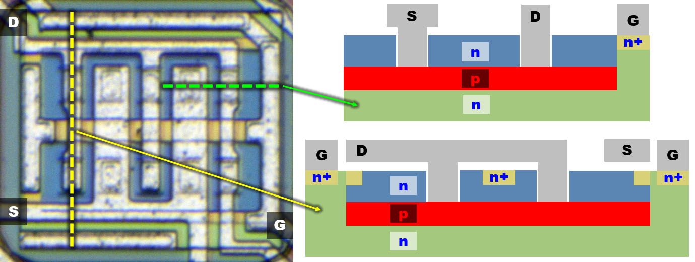


You can roughly guess the structure of the transistors. The yellowish areas are contacted by the gate potential. The drain and source lines have different widths above the transistors. But they both seem to contact a deeper layer through cutouts. Most likely this is the p-doped channel.

The blue area is then n-doped and represents the upper part of the gate. The yellowish areas are thus likely to be highly n-doped areas. The high n-doping is necessary to provide an ohmic contact with the metal layer and to avoid a Schottky contact. It also ensures a low resistance distribution of the gate potential. The gate line additionally contacts greenish areas at the upper and lower edges of the transistor. I assume that this is the lower gate electrode.
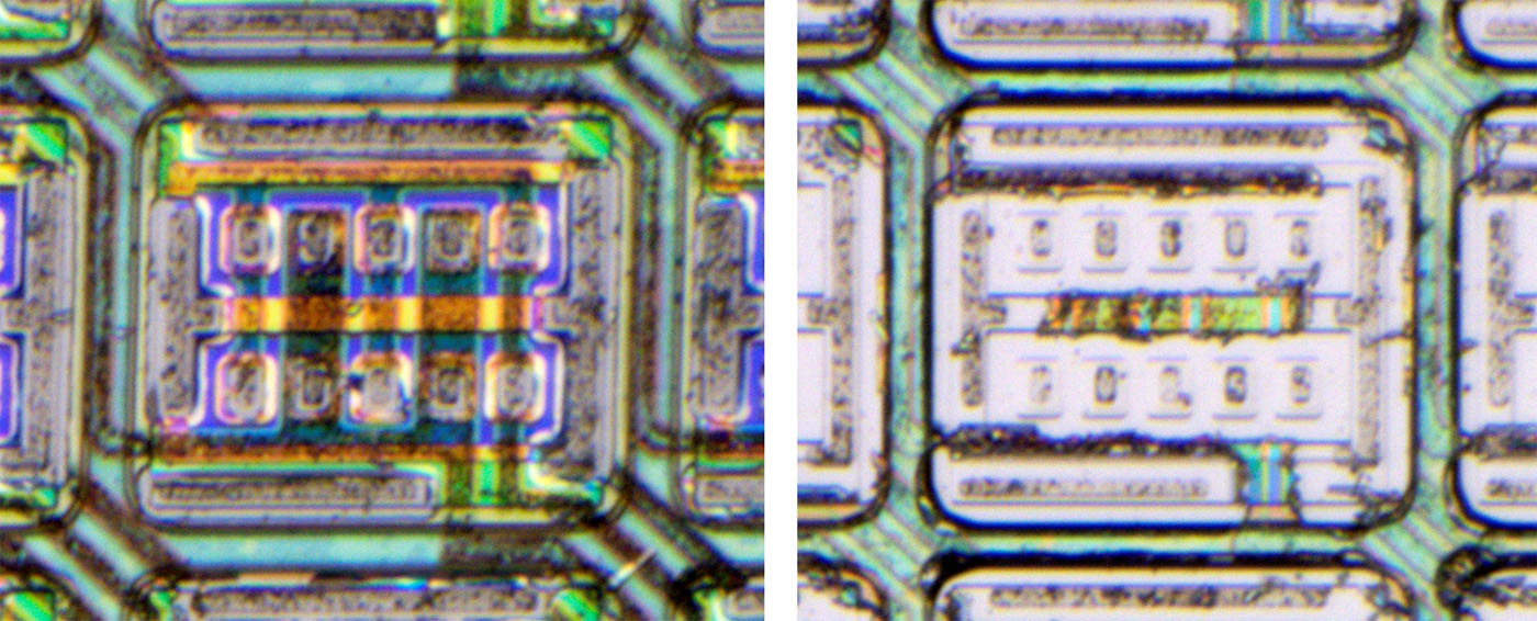


In the left image, the metal layer was removed (3min HF, 3min HCL, 15min HF). Now you can guess the drain and source contacts.

In the right image more silicon oxide was dissolved (25min HF). In the active area there are now almost no colored areas left. This indicates that the silicon level has been reached. The different colors arise just in the thin silicon oxide layers where light resonances occur.
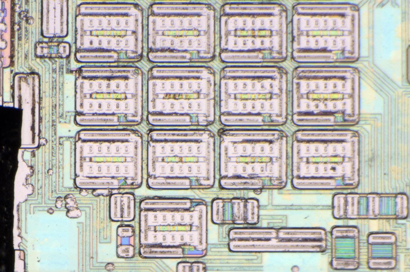


It is interesting that the frame structure still appears colored. After the silicon oxide layers have been removed, the isolation regions usually remain colorless, since they are merely inverse dopants within the substrate (see https://www.richis-lab.de/Howto_Decap_HF.htm for example). In case of the OPA627 with its dielectric isolation of the transistors, the isolation regions are deeper silicon oxide layers which have not yet been dissolved and accordingly still exhibit a slight colorfulness.
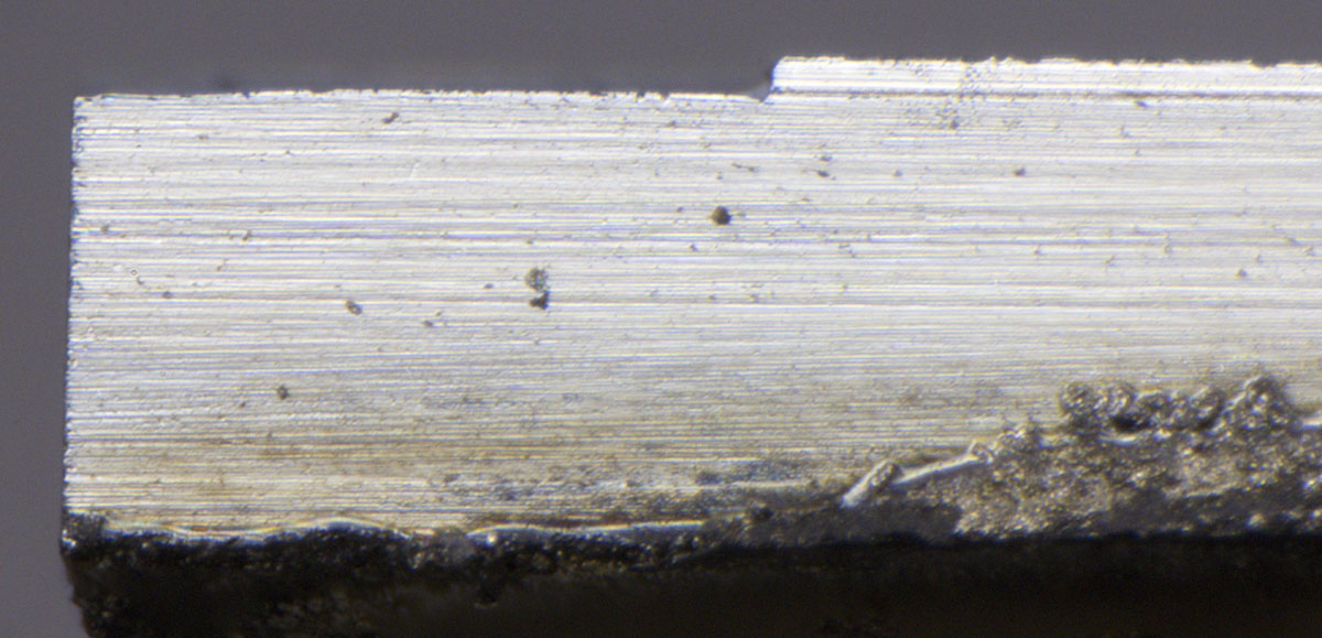
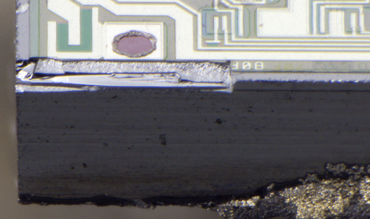


The die has suffered some damage at one edge. As described in the first OPA627 post, dielectric isolation is created by grinding a suitably prepared wafer and then bonding it to another wafer rotated by 180°. Here it seems like exactly this upper part broke off.


https://www.richis-lab.de/Opamp22.htm#OPA627x2

 :-/O
 
The following users thanked this post: SeanB, xrunner, exe, RoGeorge, floobydust

Offline floobydust

  • Super Contributor
  • ***
  • Posts: 9063
  • Country: ca
Re: Opamps - Die pictures
« Reply #261 on: May 13, 2022, 09:52:39 pm »
What had me stumped thinking it's a fake is those particular OPA627 behaved different and measured different than ones from Digi-Key, and different from OPA828, AD744 as well.
I found different resistance values and a couple substrate? diodes, where there should have been none. The parts are also not stable around unity-gain where the DK parts are fine. Same Icc.

So it looks like they are manufacturing rejects?

[ Specified attachment is not available ]
« Last Edit: May 13, 2022, 09:56:49 pm by floobydust »
 

Offline T3sl4co1l

  • Super Contributor
  • ***
  • Posts: 22435
  • Country: us
  • Expert, Analog Electronics, PCB Layout, EMC
    • Seven Transistor Labs
Re: Opamps - Die pictures
« Reply #262 on: May 14, 2022, 03:34:46 am »
Neato, so if you leave it soaking in HF, do the transistors fall off? :D

Tim
Seven Transistor Labs, LLC
Electronic design, from concept to prototype.
Bringing a project to life?  Send me a message!
 

Online magic

  • Super Contributor
  • ***
  • Posts: 8062
  • Country: pl
Re: Opamps - Die pictures
« Reply #263 on: May 14, 2022, 09:28:12 am »
You swapped sources and drains, as usual ;D
 
The following users thanked this post: Noopy

Offline NoopyTopic starter

  • Super Contributor
  • ***
  • Posts: 2401
  • Country: de
    • Richis-Lab
Re: Opamps - Die pictures
« Reply #264 on: May 14, 2022, 09:41:05 am »
So it looks like they are manufacturing rejects?

That´s possible...
I´m afraid that happens quite often. Unfortunately such parts don´t catch one´s eye immediately.  :-BROKE


Neato, so if you leave it soaking in HF, do the transistors fall off? :D

Ething for a day or two supplies you with a lot of nice J-FETs for your circuits.  ;D


You swapped sources and drains, as usual ;D

Just to check if you are still attentive.  ;D
Thanks!  :-+

Online Kleinstein

  • Super Contributor
  • ***
  • Posts: 17245
  • Country: de
Re: Opamps - Die pictures
« Reply #265 on: May 14, 2022, 11:38:09 am »
The difference in resistance is not that large. That should be well within the normal variations for the silicon resistors.
I doubt that AD would release rejects. It would be more likely to have recycled parts that may have got some initial ESD or thermal damage.
 

Offline NoopyTopic starter

  • Super Contributor
  • ***
  • Posts: 2401
  • Country: de
    • Richis-Lab
Re: Opamps - Die pictures
« Reply #266 on: May 14, 2022, 11:48:19 am »
I doubt that AD would release rejects.

I agree with you, AD won't release rejected parts but perhaps there is someone around emptying the bins and putting the scrapped parts into the market.
It seems like that happens every now and again: https://www.richis-lab.de/REF06.htm
« Last Edit: May 14, 2022, 11:50:18 am by Noopy »
 

Offline NoopyTopic starter

  • Super Contributor
  • ***
  • Posts: 2401
  • Country: de
    • Richis-Lab
Re: Opamps - Die pictures
« Reply #267 on: June 02, 2022, 07:06:13 pm »


The company George A. Philbrick Researches designed the first commercially available operational amplifier in 1953. It was built with two tubes. Later Teledyne acquired Philbrick.

The 1322 is one of a series of op-amps referred to as "optimized 741's". The 1321 and 1322 share one datasheet that describes them as "High Slew Rate Operational Amplifier". The slew rate of the 1322 is typically 80V/µs. The 1321 is much slower at 20V/µs. The bandwidth of the 1322 is up to 20MHz, while the 1321 gives you up to 120MHz. If you want to achieve high output levels you should use the 1322. For a high bandwidth the 1321 is to be preferred.

Up to a gain of 10 the opamp is stable. Below that the bandwidth has to be limited with a capacitor at pin 8. Pin 8 is very sensitive. If one wants to achieve the maximum bandwidth the datasheet recommends cutting the pin near the package to keep the parasitic capacitance low.

The bias current of the 1322 is typically 100nA, which is a low value for this category of opamp. The supply voltage may be between +/-8V and +/-20V. The 1972 Teledyne Philbrick catalog states a price of $20. Today (2022) this corresponds to a value of 140$.


In the overview you can already see that the bonding process was problematic. Failed bonds have left residues on the connection pins.


The dimensions of the dies are 1.6mm x 1.2mm. Remnants of failed bonds can be seen on the bondpads.

The symmetrically constructed input stage extends centrally from the left edge to the right edge. The output stage can be found at the lower edge, especially in the left area. Above the bondpad V+ there is a tiny capacitor which apparently represents a minimum limitation of the bandwidth as long as no additional capacitor is connected externally.

In the upper left corner are two lonely resistors. The current sink of the input stage is integrated in this area too. Probably in the 1321 these resistors are used to reduce the current of the current sink. That would reduce the slew rate too. And it would fit to the fact that the bias current of the 1321 is lower by a factor of 20 compared to the 1322.


https://www.richis-lab.de/Opamp49.htm

 :-/O
 
The following users thanked this post: SeanB, RoGeorge, ch_scr, magic

Online magic

  • Super Contributor
  • ***
  • Posts: 8062
  • Country: pl
Re: Opamps - Die pictures
« Reply #268 on: June 03, 2022, 09:10:25 am »
It looks so "optimized" that it doesn't even resemble a 741.

I can't find the datasheet, is 120MHz the bandwidth or the gain-bandwidth product at 10x gain?
Not exactly the same ;)
 
The following users thanked this post: Noopy

Offline NoopyTopic starter

  • Super Contributor
  • ***
  • Posts: 2401
  • Country: de
    • Richis-Lab
Re: Opamps - Die pictures
« Reply #269 on: June 03, 2022, 09:27:20 am »
For example:
http://www.philbrickarchive.org/1972%20product%20guide.pdf

Page 16/17:
"Small signal (unity gain, open loop), min" and "100MHz"
but hey, there is a small 2 at the 1321 stating "G x BW at A=3". :palm:

You are right.  :-+


I don´t see much 741 either.  ;D

Offline David Hess

  • Super Contributor
  • ***
  • Posts: 19215
  • Country: us
  • DavidH
Re: Opamps - Die pictures
« Reply #270 on: June 04, 2022, 08:54:25 am »
It looks so "optimized" that it doesn't even resemble a 741.

It is too bad Teledyne was so parsimonious with their datasheets but even so, it is obviously not a 741 based design; it has input bias current cancellation and the maximum differential input voltage is 12 volts.  Performance and the 12 volt differential voltage limit make it similar to a Signets 531 which has a Darlington NPN only input stage.

I do not see any mention of the 741 in the 1321/1322 datasheets but the 1332 datasheet does make a comparison to the 741 because its offset nulling configuration and unity-gain stability make it a drop in replacement.
« Last Edit: June 04, 2022, 08:57:07 am by David Hess »
 

Online magic

  • Super Contributor
  • ***
  • Posts: 8062
  • Country: pl
Re: Opamps - Die pictures
« Reply #271 on: June 04, 2022, 09:22:32 am »
There is no bias cancellation but emitter follower drivers (loaded with active sinks) in front of a heavily degenerated differential pair. That's how they got low bias and high impedance (i.e. low variation of bias with input voltage) with fast slew rate. The input stage is quite obvious.

The rest I think is a folded cascode voltage gain stage and emitter follower output (think AD829 et al) fabricated in complementary bipolar technology on dielectric isolation, like OPA627, except no JFETs and made in 1972 :o

I will have to take a closer look later.
 

Offline David Hess

  • Super Contributor
  • ***
  • Posts: 19215
  • Country: us
  • DavidH
Re: Opamps - Die pictures
« Reply #272 on: June 04, 2022, 07:52:31 pm »
There is no bias cancellation but emitter follower drivers (loaded with active sinks) in front of a heavily degenerated differential pair. That's how they got low bias and high impedance (i.e. low variation of bias with input voltage) with fast slew rate. The input stage is quite obvious.

I was going by the datasheet which lists bipolar input bias current and identical input offset current for the 1321.

Quote
The rest I think is a folded cascode voltage gain stage and emitter follower output (think AD829 et al) fabricated in complementary bipolar technology on dielectric isolation, like OPA627, except no JFETs and made in 1972 :o

I wondered if it might be a dielectric isolated process.  That plus transconductance reduction would explain the higher performance.
 

Online magic

  • Super Contributor
  • ***
  • Posts: 8062
  • Country: pl
Re: Opamps - Die pictures
« Reply #273 on: June 05, 2022, 06:38:41 am »
I wondered if it might be a dielectric isolated process.
Everything points to that. Isolation islands look very much like those on OPA627. And it has to be complementary because there are transistors that need to be PNPs for the circuit to work which don't look like the usual lateral PNPs and apparently work just fine at 20MHz.

One such process that's known to have existed in the '70s was owned by Harris and bingo, this chip appears to be rebadged HA-2520. It's a lot more complex than textbook examples or Analog's simplified schematics, but if you look closely Q24,Q23 are the current mirror, driven by Q25,Q20 emitter followers, passing its current through Q25,Q13 common base to the summing node at Q12 base, which drives the diamond buffer Q14~Q19 (no idea what's the point of the diodes Q14 level-shifts Q11 base to prevent Q12 saturation and Q18 restores proper output bias, but why is Q14 not placed above Q16 base instead?). The compensation cap at Q12 base is missing on this schematic.


Harris 1977 linear databook contains an illustration of the dielectric isolation process and their vertical PNP structure.
« Last Edit: June 05, 2022, 06:49:30 am by magic »
 
The following users thanked this post: Noopy

Offline NoopyTopic starter

  • Super Contributor
  • ***
  • Posts: 2401
  • Country: de
    • Richis-Lab
Re: Opamps - Die pictures
« Reply #274 on: June 05, 2022, 06:55:46 am »
...

Very interesting!  :-+
I assume it´s ok for you if I add some of your thoughts to my website.  :-+


Share me

Digg  Facebook  SlashDot  Delicious  Technorati  Twitter  Google  Yahoo
Smf


-->