-
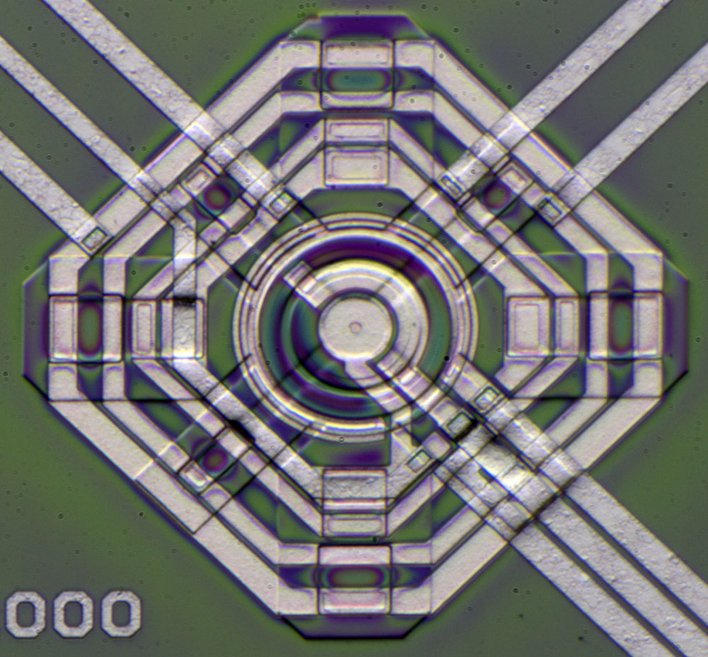
The structure in the center of the die strongly resembles the combination of Z-diode and transistor known from the LTZ1000 and the ADR1000. What seems absolutely logical at first glance raises questions when you recall the structure of this device.
I think what happens here is that the central structure is just an ordinary buried zener. There is no transistor there and no connection to the substrate. The contact in the center is a sense connection to the anode and a separate force connection ("ISET") surrounds the cathode like in ADR1000.
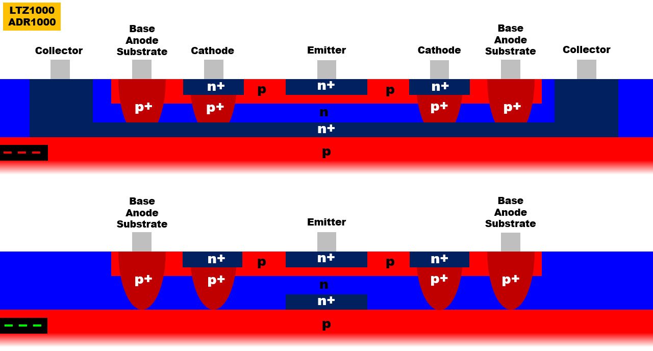
As shown in the ADR1000, the base of the transistor contacts the substrate. The emitter potential is thus more negative than the substrate. In the LTZ1000 and in the ADR1000 this is not a problem, because there are no additional circuit parts on the die apart from a transistor for temperature measurement and a heater resistor.
In the ADR1001, however, a very extensive circuit is integrated on the same die. In addition, the emitter of the Z-diode/transistor combination is connected to further circuit parts. Either the reference structure in the ADR1001 is designed differently than in the ADR1000 or a process was used in which the active structures are completely isolated from the substrate.
The multiple collector connection known from the LTZ1000 and the ADR1000 is not found here. The only contact leading to the collector layer is found at the top right. Surprisingly, the collector is connected to the base of the transistor structure.
Around the combination of Z-diode and transistor there are four more transistors. Two of the transistors (T1/T2) are used for temperature control. The other two transistors (Q2/Q3) seem to have a functional part in the voltage reference and represent the branch that one would actually look for within the special structure.
Q2 and Q3 perform the function of Q1 from ADR1000. The schematic you suggested doesn't work, because with one zener and two PN junctions in series their thermal coefficients wouldn't cancel out.I wonder where that 1.7ohm resistor at the buffer's output comes from.. Could we see it on the die?
Nothing immediately evident.
I think there is direct metal connection from BUF_F pad to the feedback network (the green R on Noopy's image, near the purple R), but those metal traces are thin so they may have significant resistance causing problems when load current flows through them. Not yet sure where exactly the output transistors are and how they are connected.
It's how ya doin'. Ideally, the feedback network should have a separate bonding wire going to the package pin or even a separate pin to include PCB parasitics (or buffers) in the feedback loop.They could have freed up one pin by removing REF6P6_F and connecting it internally to the cathode; not sure what's the point of making this connection externally.
edit
On second thought, I shouldn't suggest removing force/sense from REF6P6 when complaining about lack of force/sense on BUF. But maybe the 5V divider could be hardwired to REF6P6_S. -
..It's how ya doin'. Ideally, the feedback network should have a separate bonding wire going to the package pin or even a separate pin to include PCB parasitics (or buffers) in the feedback loop. They could have freed up one pin by removing REF6P6_F and connecting it internally to the cathode; not sure what's the point of making this connection externally.
Yep, hopefully they would do it in the ADR1002 as we discussed here earlier
-
Those beads looks like fish eggs.

Indeed!I think what happens here is that the central structure is just an ordinary buried zener. There is no transistor there and no connection to the substrate. The contact in the center is a sense connection to the anode and a separate force connection ("ISET") surrounds the cathode like in ADR1000.
Q2 and Q3 perform the function of Q1 from ADR1000. The schematic you suggested doesn't work, because with one zener and two PN junctions in series their thermal coefficients wouldn't cancel out.
Thank you for your input!
That sound very reasonable. I didn´t think of the possibility that it is just a buried zener.
I will do an update later the day. -
Nice work Noopy
Would have thought they would use 4 T-sense transistors located around the 4 corners of the zener structure similar to a cross coupled quad to control the thermal gradients within the quad interior such that the structure "sees" and iso-thermal environment in X and Y which would also require 4 heating resistors.
Anyway, the chip designers know what they are doing and guess there was no need for the extra complexity.
Great work as usual
Best, -
@Noopy: TCHIP pin - that pin is not indicated in the known pin description - there is the "NC".
In the LTSpice model there is a signal called TCHIP, which outputs the chip temperature in Celsius (at least it is my current understanding).. What that pin 2 actually does then?
Weird..
PS: it goes to the T transistor near the zener, but the signal follows also somewhere around the zener (and there is a resistor hanging on it as well).. -
@Noopy: TCHIP pin - that pin is not indicated in the known pin description - there is the "NC".
In the LTSpice model there is a signal called TCHIP, which outputs the chip temperature in Celsius (at least it is my current understanding).. What that pin 2 actually does then?
Weird..
PS: it goes to the T transistor near the zener, but the signal follows also somewhere around the zener (and there is a resistor hanging on it as well)..
In my view pin 2 is the pin to check the temperature with the transistor T. Put a Pull-Up or a current source there and you get the Vbe of the transistor.
In the schematic of the Eval-Board there is just n.c., perhaps because it´s just for internal use...
Take a closer look at the transistor, it´s just connected to TCHIP (and to GND). The two metal layers are hard to read.
-
Thanks to e61_phil for sponsering the ADR1001 for teardown and thanks for the teardown images. I see what I have expected to see, a single die solution, which confirms that ADR1000 and ADR1001 drift behavior is not comparable.
-branadic- -
Single die and different physical structure of the reference core than ADR1000.
In my view pin 2 is the pin to check the temperature with the transistor T. Put a Pull-Up or a current source there and you get the Vbe of the transistor.
That's what it looks to me as well, a simple thermal diode between TCHIP and REF_GND. Not functional without external bias and certainly not calibrated centigrade.
In the schematic of the Eval-Board there is just n.c., perhaps because it´s just for internal use...
Take a closer look at the transistor, it´s just connected to TCHIP (and to GND). The two metal layers are hard to read.
The TCHIP trace comes from north in the lower layer and connects directly with the base and collector (south).
The REF_GND trace comes from south in the upper layer, jumps through a via to the lower layer near the emitter and connects with it.
The crossing of these two traces is why it looks confusing.
Similarly confusing are the connections from BUF_F. I think it first goes north in the upper layer, then jumps to the lower layer and moves south. Near BUF_F pad it branches west in the upper layer to the output stage and also continues south to the feedback network. Hence a section of metal trace and of course bonding wire and pin are outside the loop.
The output stage looks like a bunch of paralleled emitter followers powered from VIN, so not exactly LDO. The model is wrong.
The unconnected pad under 5V divider output appears to be 2.5V. Maybe there is some lineup expansion coming
-
Isn't that bulk material sapphire? SOS technology perhaps?
And what about the resistor's material? -
Doesn't look much different from any standard nocomplementary bipolar process with NPNs and lateral PNPs.
Probably junction isolation, I think the substrate is grounded to HTR_GND and if I'm right this will need to be the lowest supply rail in the circuit.
It could be lower than REF_GND in particular. Earlier, somebody with apparent insider knowledge reported that BUF_GND can also be lower than REF_GND and -5V output from the buffer amp is officially supported.
Some sort of metal film resistors are deposited on the surface and trimmed by laser; Analog has been doing this since forever.
Visually it's all very similar to their older AD58x references from late '80s or the ADR1000. -
I have updated the pictures/text on my website with the hint magic gave us.
This is the ADR1000 structure.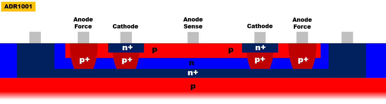
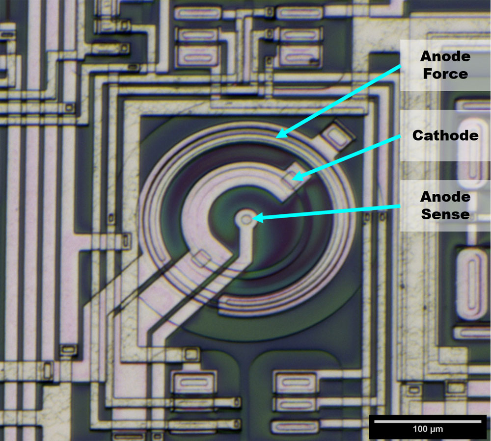
I now assume in the ADR1001 it looks like this. The emitter is missing and the contact in the middle changed to a Anode Sense.
If you look closely and compare it with the ADR1000 structure you can see that there is a ring missing. That is the emitter area.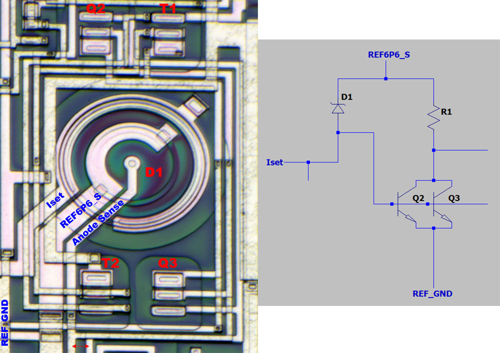
The big pictures looks like this.
https://www.richis-lab.de/REF29.htm#Update

-
You could add the connection between anode force and the isolation island to your cross section diagram.
(And link the other ADR1000 image with section lines marked on it).
Now I don't understand why they removed the transistor from there.
Substrate connection had to go for obvious reasons, but it looks like the transistor could remain inside and still work normally
-
Are you sure there is a connection between Anode Force and Substrate?
We don't see a segmented collector feed. My assumption is that the whole circuit is embedded in a closed collector well.
That would isolate the zener and on the other hand there is just a minor increase in resistance. But the resistance is not critical since we have a sense pin.
With this in mind it makes sense that they had to delete the transistor.
They had to get a Anode Sense contact and perhaps the increased base resistance (without the use of the substrate) would have been problematic. -
@Noopy: shouldn't be there p+ beneath the Anode Sense in your picture above (ADR1001)?
-
I don't see an additional structure and I don't think it is necessary.
"Normal p" has a little higher resistance but it is just the sense connection with low currents. In a transistor "normal p" is good enough for base connection too. -
An update..
Note:
34401A, 100NPLC, 10M input
7.1.23 powered off for 10minutes
24.1.23 powered off for 20minutes
18.2.23 powered off for 16 hours
5.3.23 powered off for 20minutes
17.3.23 - the first "metro-LAB measurement" Vref = 9.999.895Volt, powered off for 3 hours
-
17.3.23 - the first "metro-LAB measurement" Vref = 9.999.895Volt, powered off for 3 hours
with the same uncertainity as the other measurements? -
I expect these uncertainties of ±0.7 ppm to be a bit too overoptimistic, not sure where these are coming from.
-branadic- -
After several measurements in two labs I will evaluate.. A long way to go..17.3.23 - the first "metro-LAB measurement" Vref = 9.999.895Volt, powered off for 3 hours
with the same uncertainity as the other measurements?
-
I now assume in the ADR1001 it looks like this. The emitter is missing and the contact in the middle changed to a Anode Sense.
I'm now quite confident that this is correct indeed.
If you look closely and compare it with the ADR1000 structure you can see that there is a ring missing. That is the emitter area.
There are no meaningful connections to D1 anode-sense and Q2+Q3 base, only a reverse-biased PNP which activates under some abnormal conditions.
Q2+Q3 collector is loaded by R1 (the long resistor north-west of the reference cell) to REF6P6_S, as in usual ADR1000 applications.
There is no opamp; Q2+Q3 collector drives a sequence of two NPN inverting gain stages south of the reference cell, also resistively loaded.
The final gain stage drives a PNP emitter follower and then the NPN emitter followers at REF6P6_F output.
All other PNPs near the gain stages are reverse biased and irrelevant in normal operation.
The circuit immediately west of the reference cell looks like a bias generator.
Everything checks out. Q2+Q3 replaces the Q1 of ADR1000. -
This reverse biased pnp at D1 anode seems strange to me. I first thought it is a current sink but as you stated it doesn´t seem to act like this. But what else does this thing? Some kind of overvoltage protection?
That there is no opamp fits with my analysis. That puzzled me a little. Have to think about that...
West of the reference cell is a bias generator. I agree with that too. -
There is no absolute need of an op-amp for the voltage output. The normal circuit uses the base votlage of the Q1 resp. Q2+Q3 transistor as a more or less fixed referene point. There is not real issue in just using a seprate transistor in a high gain amplifier. A more specialized amplifier can be a bit simpler than a full single supply OP-amp.
I am not sure of the process allows for good PNPs, that maybe needed for a single supply OP-amp.
The PNP found withput an obvious purpose could be a thing for the start-up, e.g. to prevent a stable state with zero current. -
Sounds reasonable, thanks!
-
I was also surprised with the low count of transistors on the die, I expected much more stuff there TBH, but indeed you do not need full-fledged opamps for dealing with a rather limited voltage/current ranges. Would be interesting to see the schematics of the entire chip, even I doubt we will see it in the upcoming DS.
-
I expected ADR1000 with resistors integrated on-die, some cheap R2R dual opamp from Analog and a bunch of wires jumping back and forth.
Maybe the package is too small for that. Such design would also need a few MLCCs.
The reference loop is very simple. I haven't looked at thermal regulation, but there aren't too many transistor there. The buffer opamp is oddly complex, more complex than the usual OPwhatever7 we have seen in the opamps thread.
No way in hell they will bother reproducing full schematic in the datasheet. Not sure if I will bother either, but you can ask if you have specific questions. Or trace the circuitry yourself.
Regarding the "weird" pins,
TCHIP is a thermal diode, as discussed. Beware that it dumps its bias current to REF_GND, so using it may increase reference voltage by some μvolts.
PWRGD is an open collector output, its emitter also goes to REF_GND. According to eval board wiki, it only turns on during warm-up and turns off when the chip hits operating temperature.I am not sure of the process allows for good PNPs, that maybe needed for a single supply OP-amp.
They could put a whole LT1013 there. But what's the point.
The Q2+Q3 stage has ~200x gain by my estimation (any other opinions?), so Vbe stability and thermal tracking of the next stage can be 200x worse than Vbe stability of Q2+Q3.