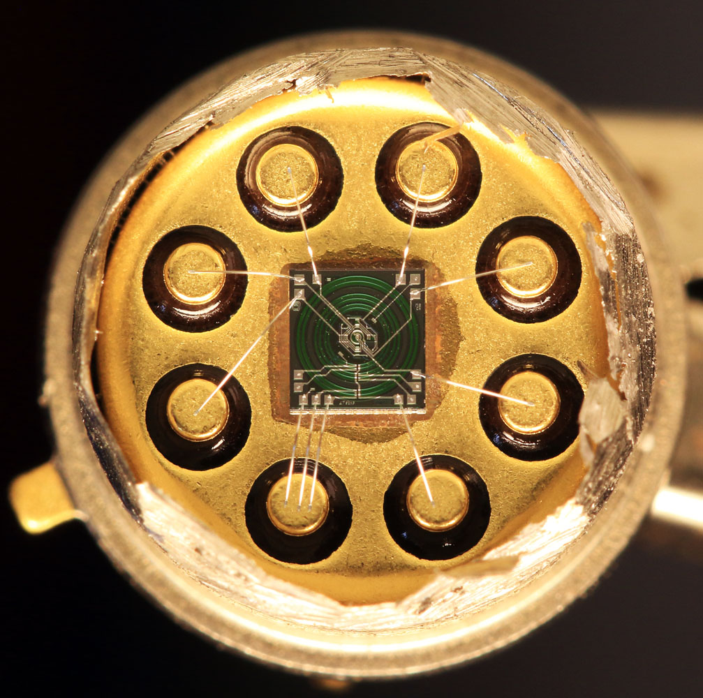
Special thanks to Noopy for braving the dangers of Hydroflouric Acid to show us more details of the chip.

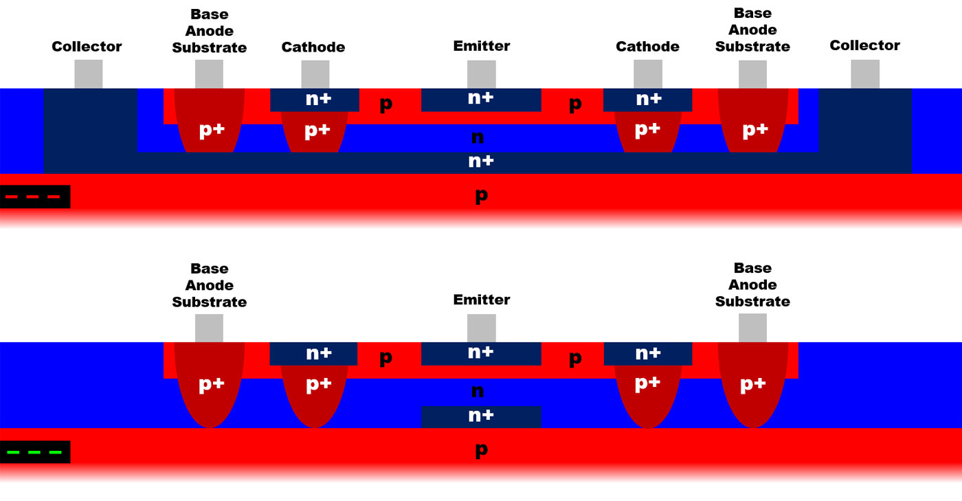
With some background information I know can tell you that this picture shows the right arrangement (in principle of course the length and width are not true to scale). 
Hmm, what sort of secret information is that?

I agree with you that this configuration would be possible and would provide us with a Kelvin connection but I don´t see a gap... 
That's a fair argument. I can't really find such gap on your photos now.
there is a square with 25 dots, is that some kind of via?
On pin 2? Not sure why there are dots but it's definitely connection between the upper (south) and lower (north) layer of metal interconnects. The two layers look slightly different and there are several other connections, but without dots.
With some background information I know can tell you that this picture shows the right arrangement (in principle of course the length and width are not true to scale).
Hmm, what sort of secret information is that?
EricM from ADI presented (MM2021) the cross sections of the heater rings and the reference breakdown region with details (the dopants profiles)..
PS: there are at least XXX people who saw the presentations.. It could be all of them signed an NDA

and therefore everything is kept secret

PPS: I was told there are only 2 pages - n.13 and n.15 related to the ADR1001 (out of 17) of Eric's presentation marked as "ADI Confidential". His presentation is not marked as "Confidential".
You are right in the heater supply there are a lot of small vias while the other vias are big squares. Interesting... Perhaps the smaller vias are better for higher currents. Perhaps there is just no reason for the difference. I can´t tell.
If memory serves me (sorry haven't routed an IC in decades)...I believe the current carrying capability of a via (in an IC) is a function of the perimeter. So the multiple small vias would have more perimeter than one big via while occupying a similar area.
What has eight legs and an eerie green glow?
My friend Jim has a home lab filled with high end microscopes. Yesterday he discovered why the ADR1000 has such fantastic performance. It is actually a Radioactive Spider at heart. A little Black Light (UV Light) shows its true identity. It’s a good thing AD keeps them locked up in the metal can.
Nikon Z6, amazing low light performance
Nikon SMZ-U Trinocular, great depth of field.
Let guess, Indium?
Not long ago I read some document about bonding stress free die attachment. Sorry, I have lost the source.
Does anyone spot this problem on the picture?
First, I thought it was interference caused by the power supply or wiring problems.
I changed another PCB that I used before , but still exists.
If I saw that here I would also be thinking wiring, supply, local disturbance etc.
I have only got one ADR powered up currently, but I haven't observed any jump or spike larger than 5uV so far.
Mobile phones can sometimes produce quite some high power interference for some sync calls, that happen not very often (e.g. 10 x a days). The output side of the LTZ/ADR1000 circuit is a bit sensitive to loading. Depending on the circuit details it may be more or less sensitive to EMI.
The capacitor at the adr1000 output (100nF in the datasheet) should be a ceramic (TH), imho. The foil capacitors do not work well at higher EMI frequencies..
Hello,
can be many root causes.
One is popcorn noise (either your instrument or the reference).
The other is EMI influence from outside (USB-cables, refrigerator, mobile phone ...)
I have the impression that the ADR1000 is more sensitive to EMI as the LTZ1000.
But I have at the moment no comparable cirquit where I can prove the impression.
I had (during 1/f noise measurement) 2-4 uV negative spikes all 15.4 seconds
which were related to a unused FTDI RS232 cable which was laying (unintentionally)
on the same desk where I did the 1/f noise measurement.
with best regards
Andreas
In the ADR pin 4 is connected directly to the case.
In the LTZ pin 4 is just connected to the die and there it connects to the substrate.
Does the special polymer die attach electrically connect the substrate and the package?
Either way EMI coupling to the ADR package adds directly to your reference voltage. LTZ looks a little more robust.
I think operating a mobile phone close to the vref is a good check.. For such frequencies even 100nF ceramics do not work well. You would need something like quality 1nF ceramic smd. Mind the ceramic smd capacitors generate voltage under mechanical stress..
In the ADR pin 4 is connected directly to the case.
In the LTZ pin 4 is just connected to the die and there it connects to the substrate.
..
I can see a bond wire from the pin 4 to the case in the LTZ..
..
That's just a part of the package that originated due to the grinding.
Pin 4 is at 4 o'clock.
Now, what would the experts say on the "grounding vs. not grounding the ref case" ? Would be interesting to know..
That's an interesting difference between the LTZ and the ADR.
In an ideal environment that doesn't matter but in real life...