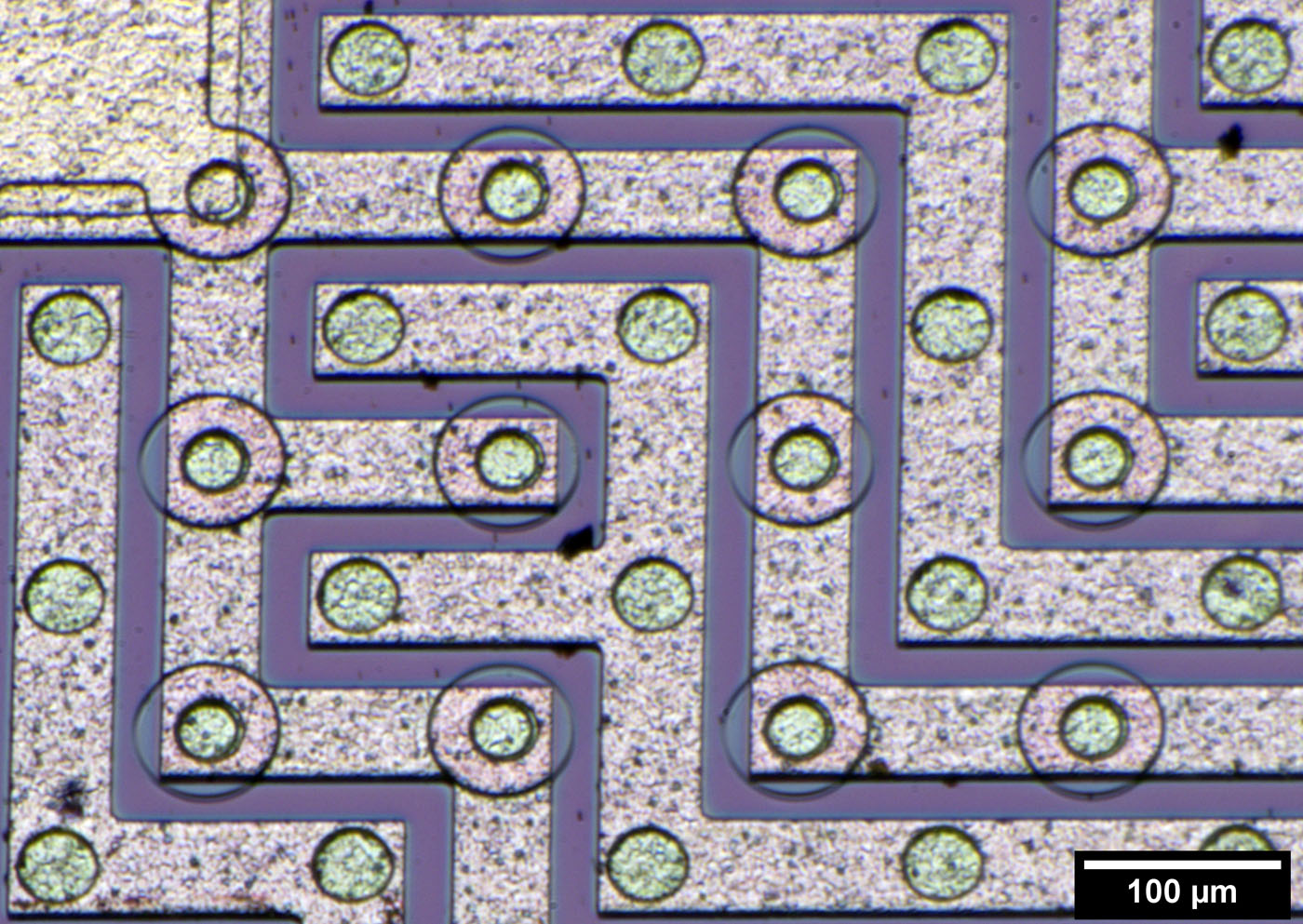
You connect the base over the whole die through perforations of the emitter. That gives you a better current Distribution and that leads to lower saturation voltage and second breakdown appears later.
Here you have more perforated emitter:
https://www.richis-lab.de/2SC2922.htm
https://www.richis-lab.de/Bipolar08.htm
Richie,
do you by accident have an 2N2857 at hand ?
I would be curious about this one.
Regards
Wolfgang
You connect the base over the whole die through perforations of the emitter. That gives you a better current Distribution and that leads to lower saturation voltage and second breakdown appears later.
Here you have more perforated emitter:
https://www.richis-lab.de/2SC2922.htm
https://www.richis-lab.de/Bipolar08.htm
Thank you @Noopy, those articles taxed my German vocabulary to the limit, aber es ist etwas gut!
do you by accident have an 2N2857 at hand ?
I would be curious about this one.
Hm... Have to take a look at my huge inbox. Got a lot of transistors the last few weeks.

Thank you @Noopy, those articles taxed my German vocabulary to the limit, aber es ist etwas gut!
Sorry for the german text but english would take me twice the time and I have so much more parts here.

A HF-Power-Transistor (the big one for GSM stations), a 18Bit-DAC, a 7,5A linear Regulator, a huge opamp and a looooot of smaller but also interesting parts.
I hope Google translator can help a bit and you can ask me here whatever you want.

Not a problem, es macht mir vergnugt to read your articles in German (aided by Google if I get stuck)
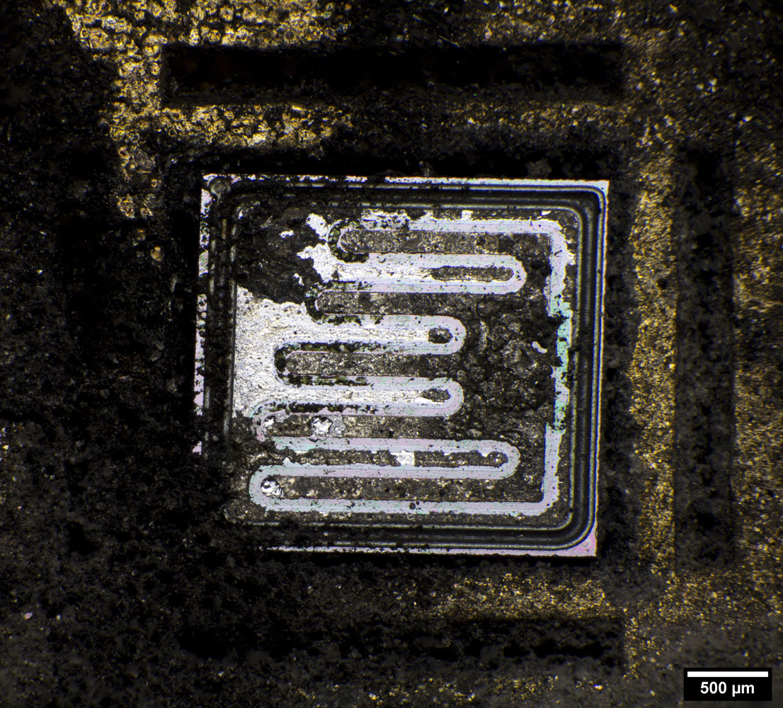
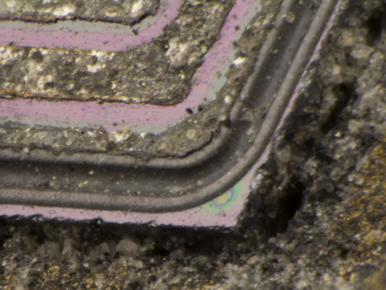
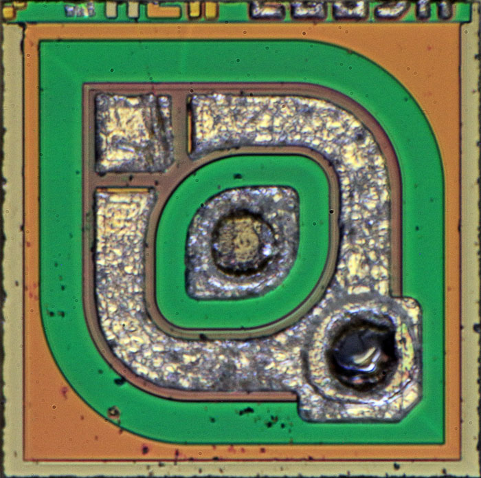
Today I have a TIP2955 for you. It´s the complementary transistor to the TIP3055.
https://richis-lab.de/Bipolar11.htm
It looks very similar to the TIP3055 and has exactly the same dimensions.
The perforated emitter looks a bit different. You can see less circles in the "holes" than in the TIP3055. Unfortunatelly I don´t know how exactly the structures are built.

The TIP2955 came form exe.
Thank you very much, this explains why some complementary pairs have very tight parameter matching (e.g., base capacitance). For some reason I expected NPN devices to be smaller for the same power rating. Either this is simply not true, or manufacturing process is well tuned.
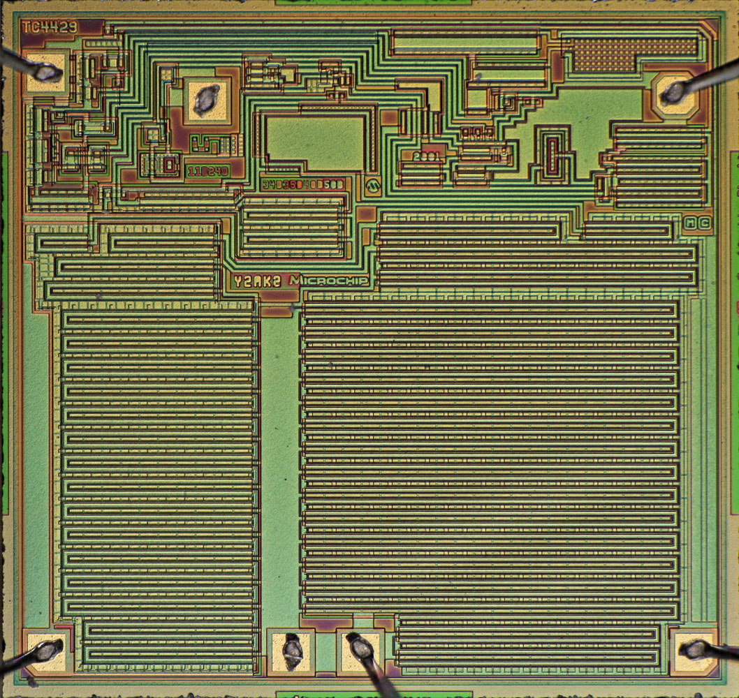
I have often seen mosfets where the p-type is bigger than the n-type. Last time in the TC4429.
I have often seen schematics where the pnp is doubled to achieve the same specifications than the npn.
But as we can see here it´s also possible to design the complementary transistors very similar.
Perhaps it´s a matter of priorities. Perhaps you can design complementary transistors equal but it´s easier to make the "p-type" bigger...

NPN and PNP with similar build (i.e., those will be N and P substrate, then P/N, then N/P, epitaxy or diffusion) have similar properties. PNP is only like 10-20% lower performance, I've forgotten exactly why now but clearly electrons and holes participate in the same way and mobility is a smaller factor in operation.
Want to say base diffusion is the only step in a BJT where mobility really matters, and the base can simply be made thinner if needed. If that's the case, we might expect to find stronger Early effect; or, it's further compensated by collector doping profile, with subtle effects on breakdown voltage, Ccb(Vcb) and voltage drop, Idunno.
If a process is limited by shitty (usually lateral) PNP, large areas might be needed to compensate for that.
Complementary MOSFETs will always differ by about a factor of two, because mobility is a direct proportion in their performance.
Tim
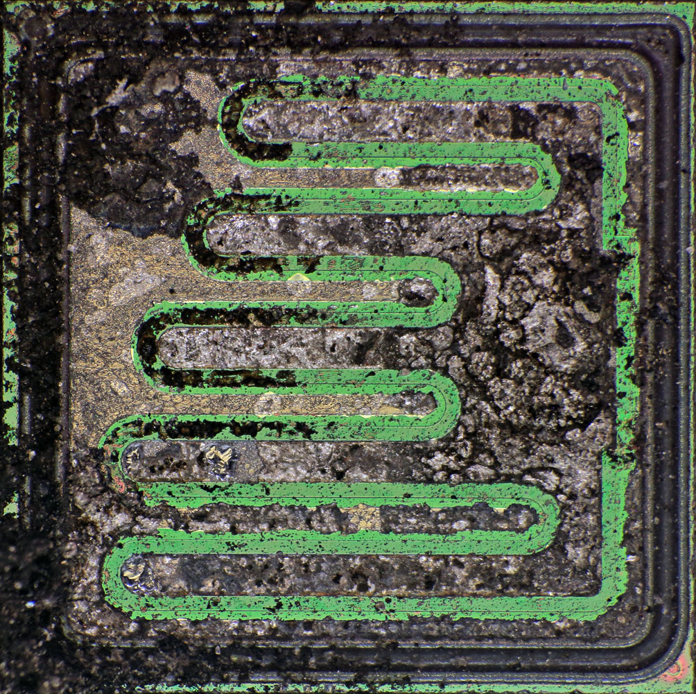
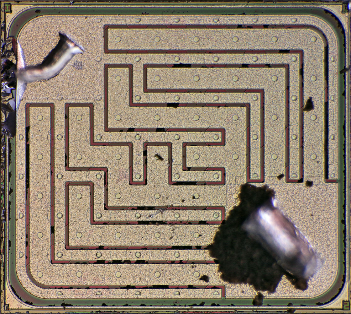
Today I can show you a TIP2955 built by ON-Semi:
https://richis-lab.de/Bipolar11.htm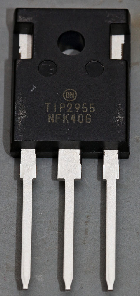
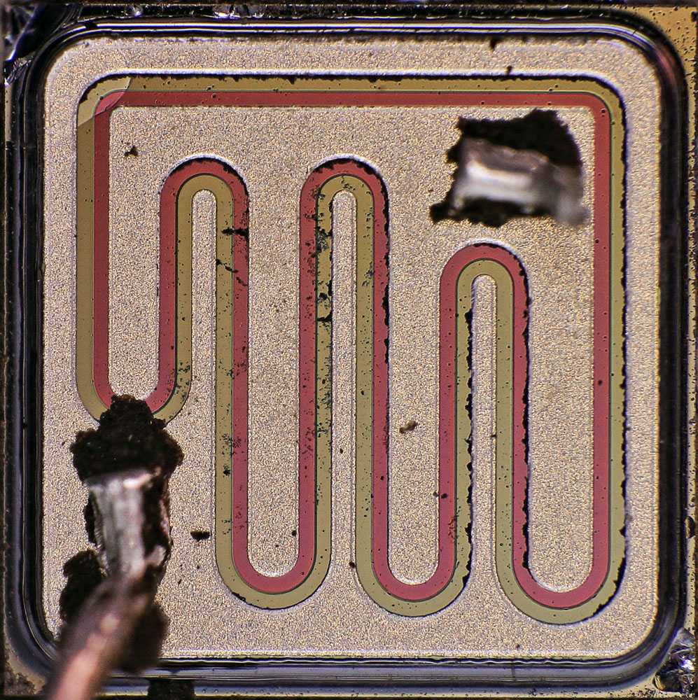
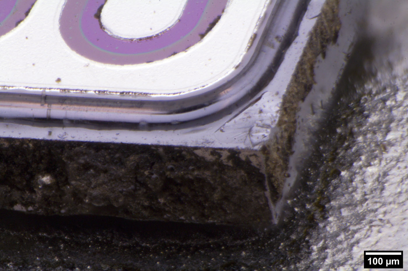
The die shows a classical construction. It is bigger (2,53mm*2,53mm) than the die in the ST-TIP2955 (2,42mm*2,15mm). I assume that´s because the classical design is less efficient than the perforated emitter design.
A MESA-structure...

The TIP2955 came form exe.
Very interesting, thank you. My measurements showed that sy parts are a bit better than onsemi parts in terms of frequency response. Perhaps, due to smaller geometry. I think it's a trend, so I expect all ST bjts will be slightly smaller than onsemi.
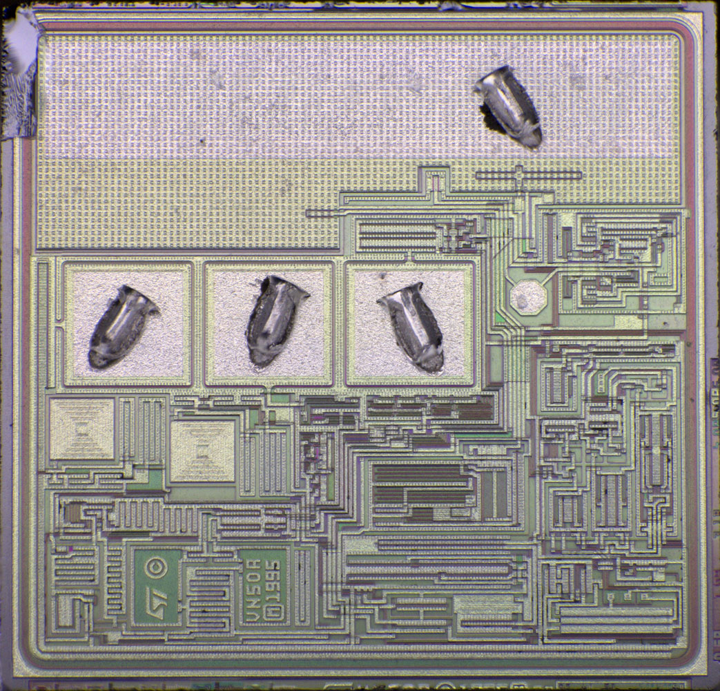
Today I have a SMART-Highside-MOSFET for you: VN02H
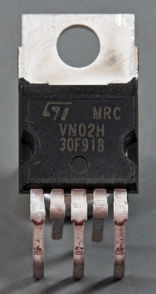
Everything on one die. That´s cool but gives you a clamping voltage of only -4V. There are special variants with -18V but that´s still not very much.
(picture taken from application note and modified)
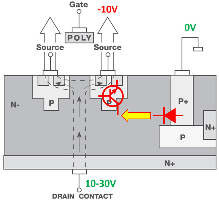
Do you know why integrated SMART-Highside-Driver have low clamping voltages?
There is a parasitic bipolar transistor between the power transistor and the barrier around the logic part that is connected to the ground potential. You don´t need very much voltage to break the collector-emitter-line and kill the part.
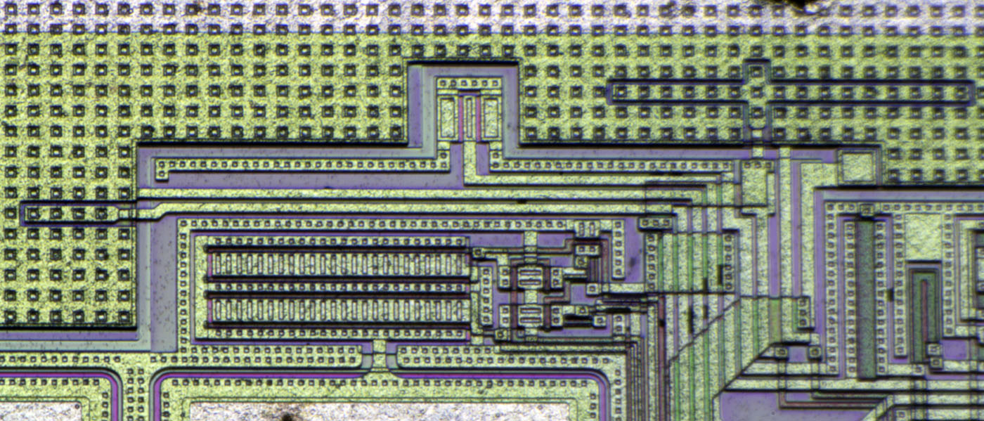
The datasheet explains that the overcurrent detection is done with the temperature meassurement (this small satellite) but it seems that there are two small MOSFETs. Theses small MOSFETs can be used to sense the current through the VN02H...
And I have a dead one.
It switched a short circuit.
The ground bondwire acted as a fuse. You can see a colored spot in the transistor area too.
Perhaps there was a overcurrent damage in the transistor and then the rest of the VN02H failed shorting the supply.
Perhaps there was somehow a transient overvoltage which killed the control part and then the power Transistor died.
We will never now for sure.
More Pictures here:
https://richis-lab.de/FET02.htm
Do you know why integrated SMART-Highside-Driver have low clamping voltages?
There is a parasitic bipolar transistor between the power transistor and the barrier around the logic part that is connected to the ground potential. You don´t need very much voltage to break the collector-emitter-line and kill the part.
I assume the dielectricly isolated process used for DMOS would be too expensive in both fabrication and area.
The datasheet explains that the overcurrent detection is done with the temperature meassurement (this small satellite) but it seems that there are two small MOSFETs. Theses small MOSFETs can be used to sense the current through the VN02H...
That is a very common technique for CMOS power devices and 4 pin power MOSFETs which allow monitoring the current. A few cells of the power MOSFET have a separate drain connection brought out and the ratio of areas determines the fraction of the drain current which is detected.
It also works for bipolar devices.
Wow, surprised they waste so much die area on control logic!
Tim
An LM395 die shot would be interesting and I think I have seen it somewhere. As I recall, it was very similar to the LM317 and might have been the same die with a different metalization.
Do you know why integrated SMART-Highside-Driver have low clamping voltages?
There is a parasitic bipolar transistor between the power transistor and the barrier around the logic part that is connected to the ground potential. You don´t need very much voltage to break the collector-emitter-line and kill the part.
I assume the dielectricly isolated process used for DMOS would be too expensive in both fabrication and area.
And with dielectric isolation you can´t build the more powerful vertical DMOS, can you?
The datasheet explains that the overcurrent detection is done with the temperature meassurement (this small satellite) but it seems that there are two small MOSFETs. Theses small MOSFETs can be used to sense the current through the VN02H...
That is a very common technique for CMOS power devices and 4 pin power MOSFETs which allow monitoring the current. A few cells of the power MOSFET have a separate drain connection brought out and the ratio of areas determines the fraction of the drain current which is detected.
I know this kind of current measurement. It just surprised me that the datasheet by contrast explains a temperature based overcurrent detection.
An LM395 die shot would be interesting and I think I have seen it somewhere. As I recall, it was very similar to the LM317 and might have been the same die with a different metalization.
I will put the LM395 on my to-do-list.
Do you know why integrated SMART-Highside-Driver have low clamping voltages?
There is a parasitic bipolar transistor between the power transistor and the barrier around the logic part that is connected to the ground potential. You don´t need very much voltage to break the collector-emitter-line and kill the part.
I assume the dielectricly isolated process used for DMOS would be too expensive in both fabrication and area.
And with dielectric isolation you can´t build the more powerful vertical DMOS, can you?
No, I don't think you can but the lateral power devices can still be very powerful. Their disadvantage is that they take much more area. On the other hand, they have much lower capacitance.
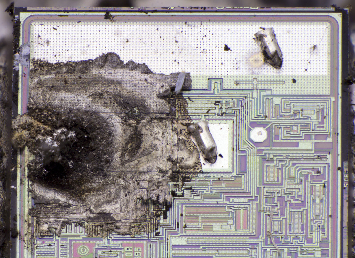
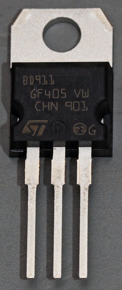
Hi all!
Today I have a BD911 for you. It is quite simliar to the TIP3055 (
https://richis-lab.de/Bipolar10.htm). The collector-emitter-voltage and the hfe are a bit higher for the BD911.
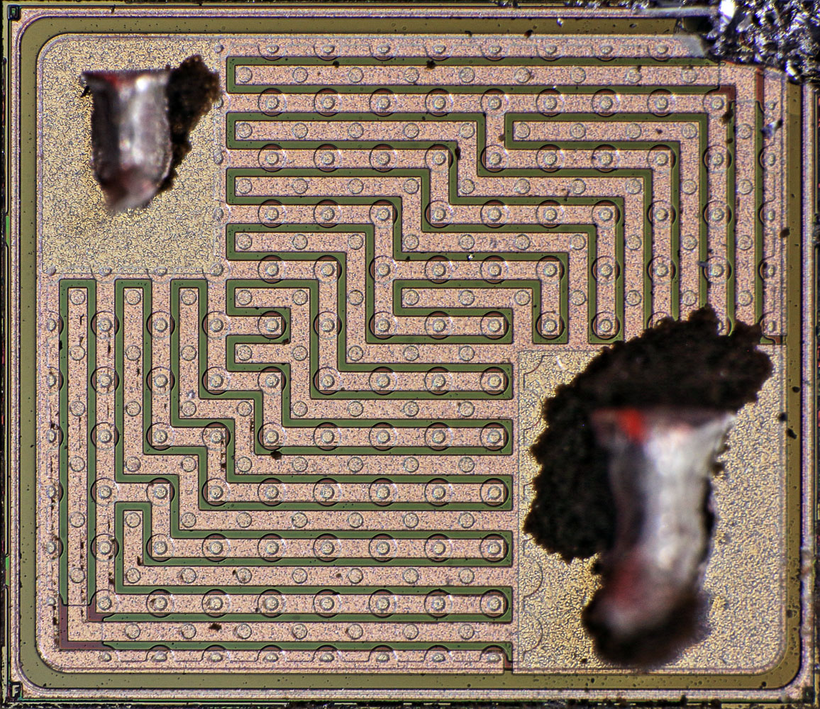
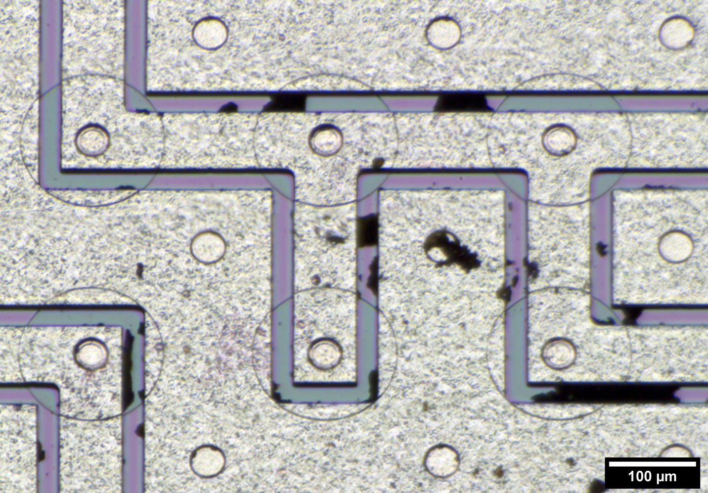
The die is similar to the die in the TIP3055 but it´s smaller (4,66mm² vs. 5,25mm²) although it has the better specifications.
In my view ST was able to enhance the specificatons of the stackup. Probably the more close meshed perforation improves also the specifications.
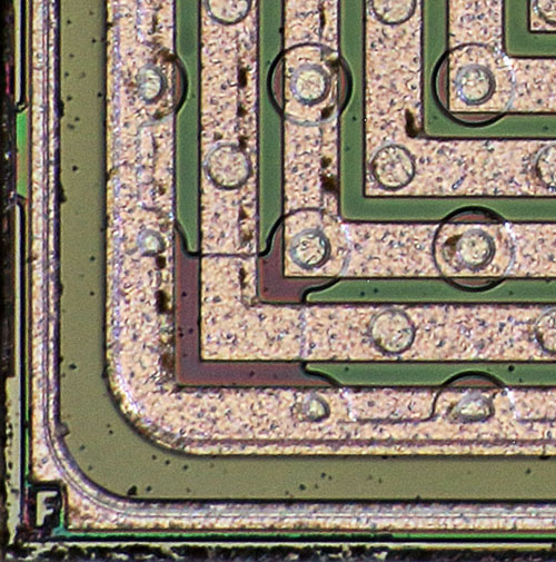
I think they did some potential steering in the corners of the die.
The perforations are quite small compared to the TIP3055.
https://richis-lab.de/Bipolar12.htmPart was donated by exe.
Very interesting, the die is smaller, however it looks like the "labyrinth" has more total length. I wonder which one has less parasitic capacitance.
Anyway, which one would be prefered for a linear power supply and why?

My read is that the BD911 has less capacitance.
Less area => Less capacitance.
But perhaps the SOA of the BD911 is smaller. A smaller die is often heavier donated. But that´s only a guess…
Hard to decide which on is better for a linear power supply. BD911 has a higher voltage rating but perhaps TIP3055 has a bigger SOA...
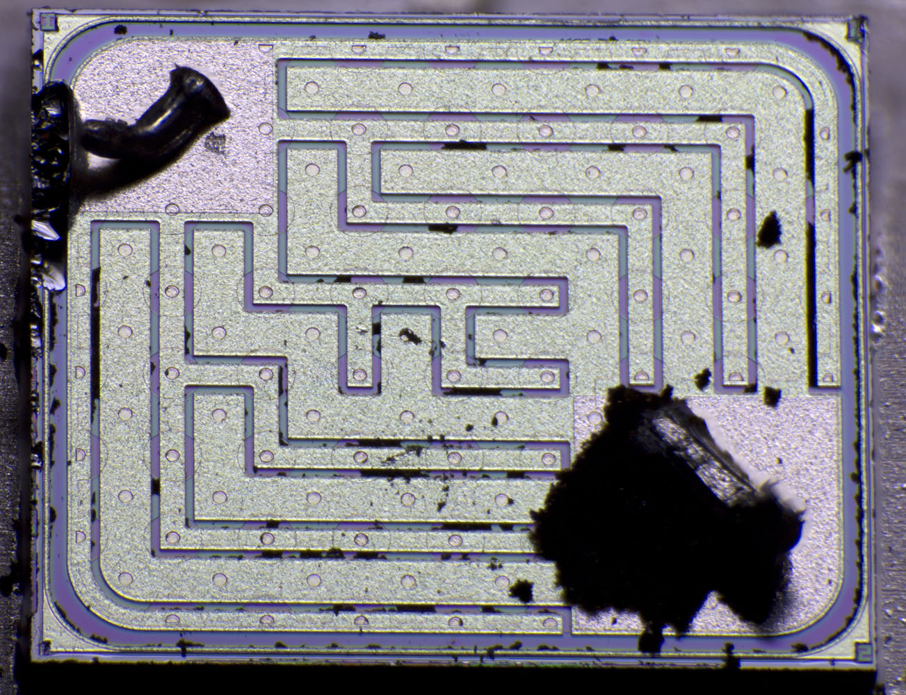
A classical mesa-design but OnSemi uses it still today for the TIP2955:
https://www.richis-lab.de/Bipolar11.htm
I was under the impression that the mesa process was long discontinued, except maybe for premium parts, because it is too expensive due to the time it takes to manufacturer.
A classical mesa-design but OnSemi uses it still today for the TIP2955:
https://www.richis-lab.de/Bipolar11.htm
I was under the impression that the mesa process was long discontinued, except maybe for premium parts, because it is too expensive due to the time it takes to manufacturer.
Perhaps it´s still cheaper than for example manufacturing a perforated emitter?
Perhaps there is an old production line working at a very reasonable price?
Today I have a very special transistor, the Programmable Unijunction Transistor 2N6027:
The die is very small: 440µm x 440µm.
However for 10µs a peak current of 5A is allowed.
These transistors are still in production.