Quick Links:
#2446: buergi's "information needed to memdump [a] DS2KA"
All the talk of Rigol hacks got me curious about what goes on inside my DS1102E's non-volatile RAM. There's a
FM24CL04 chip on the main board and as a prelude to hacking some more expensive equipment, I thought I'd break out the soldering iron and turn my 1102E into a guinea pig:

A logic analyzer shows decodable activity on those lines. Here's (the first part) of what happens when I change the timebase from 20ms/div to 50ms/div:
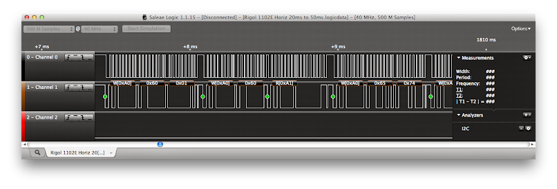
I'm not sure how to decipher it yet, but since the horizontal timebase is restored on power-up, the I2C activity is probably how the mcu saves that particular piece of information.
Attached is a .zip with two logic analyzer (Saleae Logic16) dumps. The small one is when I changed the horiz timebase. The big one is what goes on when the scope boots up.
Does anyone have suggestions on a good way to decode this data? The Saleae app seems OK, but it's hard to see more than a few bytes on the screen at once. It'd be much nicer to get a text dump of reads/writes by address.
PS. I forgot to probe the two address pins on the FRAM chip while I had the case open.

I suspect they're wired to GND though. I.e., the FRAM will be responsive to addresses like 0b101000XX.
Don't have a Salea, never used their software before...
I downloaded it, opened one of the files, clicked on the 'gear' next to I2C, clicked export... The format of the generated text file isn't spectacular (the formatting of the 'data' column is annoyingly inconsistent). But, thats nothing a few lines of python/perl couldn't fix
Something like a Bus Pirate, or Arduino or whatever that has a hardware I2C interface. As I understand it, most of these USB analyzers rely on buffering and can't do 'realtime' decoding, or store enough samples to capture long or infrequent-ish events.
I would first get a full image of the FRAM, and then decode each change and map controls (e.g. vertical gain) to bytes in the memory. Hopefully you can build a map of what goes where, which will get you started on figuring out what values mean what. If the DS1102 firmware is similar to the DS2000 series, it will read the entire FRAM sequentially at boot.
I'll have a Bus Pirate sometime next week.
Just looking at the amount of stuff that goes by at boot, I'd guess that the 1102 is reading the entire FRAM too. Calculating a checksum, maybe?
Has someone done a similar experiment with the DS2000/4000? Ultimately, that's where I'm headed. But if I'm going to brick a scope, I'd rather it be a cheap one.

I'll have a Bus Pirate sometime next week.
When I did this I had to dick around with custom (faster than the firmware lets you set) baud rates to get it to be fast enough during the long initial read. It did end up working well enough to capture the bootup though; a quick Python hack and I had a binary image file.
Just looking at the amount of stuff that goes by at boot, I'd guess that the 1102 is reading the entire FRAM too. Calculating a checksum, maybe?
The DS2000 has a checksum. IIRC it was CRC32 in the last 4 bytes, but whatever it was it was trivial to find. So that's probably a good guess.
Has someone done a similar experiment with the DS2000/4000? Ultimately, that's where I'm headed. But if I'm going to brick a scope, I'd rather it be a cheap one.
I did, but I just used clip leads and didn't leave it permanently connected. Kept it on for long enough to capture an image but that's about it, I needed to use the scope
.
Of course, but what's on my bench at the moment is an 1102E. There are already reasons to believe that the non-volatile storage implementations are similar between the different Rigol scope families. So poking around on a cheap unit should make it easier to understand what's happening in the more expensive models.
Questions to be answered:
- Is there a CRC in NVRAM? If so, where is it stored and which algorithm?
- What does the firmware do when it detects a bad CRC?
- What's the "spec" for updating a single value?
- Which values are actually stored in NVRAM?
- Can we put together a "memory map" of known values including their offsets and lengths.
- Can the NVRAM chip be written to without removing it from the main board?
- Are any of the programming headers directly attached to the NVRAM?
anyone yet tried to find out the segmentation of the firmware file for a DS2000 ?
i have compared 00.00.01.00.05 with 00.01.00.00.03 - and in the first chunks there is a large similarity, there is around 0x30000 bytes of blackfin code which is very similar, except a few offset bytes for lower half registers. also in there seem to be the bitstreams for the xilinx fpga (0xAA 0x99 0x55 0x66 header).
it seems to use lwip (there is plenty of AD sample code), embedded GoAhead-webs (Webserver), VDK threads
so far i was unable to get any sense, besides a chunk counter, out of the file headers.
it would be helpfull if somebody could provide a 3rd firmware release
so far no plans in touching the actual hardware. there also seem to be some exploits for the goahead webserver, which might be a way to get remote code execution.
DS2000_1.GEL
============

44 53 32 32 30 32 00 00 00 00 00 00 00 00 00 00 30 30 2E 30 30 2E 30 31 2E 30 30 2E 30 35 00 {VERSION HEADER}

                  number of "simliar" looking chunks
                 /
00 07 00 00 00 11 00 00 00 B4 3D 31 00 04 02 00 00 63 7C 37 17 00 00 00 00 00 00 04
20 01 00 00 00 00 00 00 00 58 BD 17 00 B8 3F 31 00 B6 96 14 05 06 00 00 00 00 00 00
20 05 00 00 00 00 00 00 00 60 0F 01 00 10 FD 48 00 6B A4 C1 52 02 00 00 00 00 00 00
20 0A 00 00 00 00 00 00 00 78 1B 03 00 70 0C 4A 00 CE F9 DD 2B 02 00 00 00 00 00 02
20 0B 00 00 00 00 00 00 00 5A 24 00 00 E8 27 4D 00 25 73 2A CD 02 00 00 00 00 60 0D
20 0C 00 00 00 00 00 00 00 F4 78 00 00 42 4C 4D 00 D5 06 98 0E 04 00 00 00 00 80 0C
20 0E 00 00 00 00 00 00 00 E8 B6 05 00 36 C5 4D 00 74 D1 E8 0E 04 00 00 00 00 A0 0F
20 0F 00 00 00 00 00 00 00 54 1D 00 00 1E 7C 53 00 9E 58 B8 BC 02 00 00 00 00 00 12
20 10 00 00 00 00 00 00 00 68 2E 06 00 72 99 53 00 46 63 39 BB 04 00 00 00 00 00 00
20 11 00 00 00 00 00 00 00 4C 30 00 00 DA C7 59 00 C9 49 90 3B 03 00 00 00 00 00 04
20 13 00 00 00 00 00 00 00 64 0B 00 00 26 F8 59 00 F5 95 B6 D2 05 00 00 00 00 00 00
20 14 00 00 00 00 00 00 00 98 C5 03 00 8A 03 5A 00 CC 1B 1C 3F 05 00 00 00 00 0C 00
20 15 00 00 00 00 00 00 00 18 01 00 00 22 C9 5D 00 9D DF F2 1A 05 00 00 00 00 4C 1E
20 15 00 00 00 00 00 00 00 1C 90 00 00 3A CA 5D 00 39 A5 80 1A 05 00 00 00 00 D4 03
20 15 00 00 00 00 00 00 00 61 16 00 00 56 5A 5E 00 E1 CE 61 51 03 00 00 00 00 D8 1F
20 15 00 00 00 00 00 00 00 08 B8 0B 00 B7 70 5E 00 40 0B 53 4B 03 00 00 00 00 50 04
20 15 00 00 00 00 00 00 00 00 00 00 00 BF 28 6A 00 00 00 00 00 02 00 00 00 00 28 12
20 32 00 00 00 00 00 00 00 06 50 18 AD 00 00 A0 FF 00 00 00 00 BC 00 00 00 06 00 E8
AD 00 80 A0 FF
{BLACKFIN CODE, SDRAM controller init ...}

DS2000_2.GEL
============

44 53 32 32 30 32 00 00 00 00 00 00 00 00 00 00 30 30 2E 30 31 2E 30 30 2E 30 30 2E 30 33 00 {VERSION HEADER}

00 07 00 00 00 12 00 00 00 9C 8F 37 00 20 02 00 00 7E 42 E9 27 00 00 00 00 00 00 04
20 01 00 00 00 00 00 00 00 A8 CC 17 00 BC 91 37 00 C3 C3 3A 5A 06 00 00 00 00 00 00
20 05 00 00 00 00 00 00 00 60 0F 01 00 64 5E 4F 00 6B A4 C1 52 02 00 00 00 00 00 00
20 0A 00 00 00 00 00 00 00 AA 21 03 00 C4 6D 50 00 8A F3 49 6C 02 00 00 00 00 00 02
20 0B 00 00 00 00 00 00 00 5A 24 00 00 6E 8F 53 00 25 73 2A CD 02 00 00 00 00 60 0D
20 0C 00 00 00 00 00 00 00 B4 7F 00 00 C8 B3 53 00 70 78 AC 4C 04 00 00 00 00 80 0C
20 0E 00 00 00 00 00 00 00 F4 63 06 00 7C 33 54 00 80 5A 4D 45 04 00 00 00 00 00 0F
20 0F 00 00 00 00 00 00 00 54 1D 00 00 70 97 5A 00 9E 58 B8 BC 02 00 00 00 00 00 12
20 10 00 00 00 00 00 00 00 62 DC 06 00 C4 B4 5A 00 98 8C 5A 88 04 00 00 00 00 00 00
20 11 00 00 00 00 00 00 00 D8 32 00 00 26 91 61 00 18 1D 48 B7 03 00 00 00 00 00 04
20 13 00 00 00 00 00 00 00 64 0B 00 00 FE C3 61 00 F5 95 B6 D2 05 00 00 00 00 00 00
20 14 00 00 00 00 00 00 00 98 C5 03 00 62 CF 61 00 CC 1B 1C 3F 05 00 00 00 00 0C 00
20 15 00 00 00 00 00 00 00 18 01 00 00 FA 94 65 00 9D DF F2 1A 05 00 00 00 00 4C 1E
20 15 00 00 00 00 00 00 00 10 90 00 00 12 96 65 00 A2 35 07 55 05 00 00 00 00 D4 03
20 15 00 00 00 00 00 00 00 61 16 00 00 22 26 66 00 E1 CE 61 51 03 00 00 00 00 D8 1F
20 15 00 00 00 00 00 00 00 08 B8 0B 00 83 3C 66 00 40 0B 53 4B 03 00 00 00 00 50 04
20 15 00 00 00 00 00 00 00 F0 6E 04 00 8B F4 71 00 FB ED C4 52 07 00 00 00 00 00 10
20 15 00 00 00 00 00 00 00 00 00 00 00 7B 63 76 00 00 00 00 00 02 00 00 00 00 28 12
20 32 00 00 00 00 00 00 00 06 50 18 AD 00 00 A0 FF 00 00 00 00 BC 00 00 00 06 00 E8
AD 00 80 A0 FF
{BLACKFIN CODE, SDRAM controller init ...}

SDRAM controller init code ... (same for both files)

 21c:   9c 00          RAISE 0xc;
     21e:   00 00          NOP;
     220:   00 00          NOP;
     222:   00 00          NOP;
     224:   66 01          [--SP] = ASTAT;
     226:   67 01          [--SP] = RETS;
     228:   40 05          [--SP] = (R7:0);
     22a:   c0 04          [--SP] = (P5:0);
     22c:   50 01          [--SP] = I0;
     22e:   51 01          [--SP] = I1;
     230:   52 01          [--SP] = I2;
     232:   53 01          [--SP] = I3;
     234:   58 01          [--SP] = B0;
     236:   59 01          [--SP] = B1;
     238:   5a 01          [--SP] = B2;
     23a:   5b 01          [--SP] = B3;
     23c:   54 01          [--SP] = M0;
     23e:   55 01          [--SP] = M1;
     240:   56 01          [--SP] = M2;
     242:   57 01          [--SP] = M3;
     244:   5c 01          [--SP] = L0;
     246:   5d 01          [--SP] = L1;
     248:   5e 01          [--SP] = L2;
     24a:   5f 01          [--SP] = L3;
     24c:   08 e1 18 0a    P0.L = 0xa18;      /* (2584)   P0=0xa18 */
     250:   48 e1 c0 ff    P0.H = 0xffc0;      /* (-64)   P0=0xffc00a18(-4191720) */
     254:   80 e1 ff ff    R0 = 0xffff (Z);      /*      R0=0xffff(65535) */
     258:   00 97          W[P0] = R0;
     25a:   24 00          SSYNC;
     25c:   08 e1 14 0a    P0.L = 0xa14;      /* (2580)   P0=0xffc00a14(-4191724) */
     260:   48 e1 c0 ff    P0.H = 0xffc0;      /* (-64)   P0=0xffc00a14(-4191724) */
     264:   80 e1 13 00    R0 = 0x13 (Z);      /*      R0=0x13( 19) */
     268:   00 93          [P0] = R0;
     26a:   24 00          SSYNC;
     26c:   08 e1 10 0a    P0.L = 0xa10;      /* (2576)   P0=0xffc00a10(-4191728) */
     270:   48 e1 c0 ff    P0.H = 0xffc0;      /* (-64)   P0=0xffc00a10(-4191728) */
     274:   00 e1 8d 99    R0.L = 0x998d;      /* (-26227)   R0=0x998d(39309) */
     278:   40 e1 91 00    R0.H = 0x91;      /* (145)   R0=0x91998d(9542029) */
     27c:   00 93          [P0] = R0;
     27e:   24 00          SSYNC;
     280:   08 e1 00 0a    P0.L = 0xa00;      /* (2560)   P0=0xffc00a00(-4191744) */
     284:   48 e1 c0 ff    P0.H = 0xffc0;      /* (-64)   P0=0xffc00a00(-4191744) */
     288:   00 e1 ff 01    R0.L = 0x1ff;      /* (511)   R0=0x9101ff(9503231) */
     28c:   40 e1 00 00    R0.H = 0x0;      /* (  0)   R0=0x1ff(511) */
     290:   00 93          [P0] = R0;
     292:   24 00          SSYNC;
     294:   1f 01          L3 = [SP++];
     296:   1e 01          L2 = [SP++];
     298:   1d 01          L1 = [SP++];
     29a:   1c 01          L0 = [SP++];
     29c:   17 01          M3 = [SP++];
     29e:   16 01          M2 = [SP++];
     2a0:   15 01          M1 = [SP++];
     2a2:   14 01          M0 = [SP++];
     2a4:   1b 01          B3 = [SP++];
     2a6:   1a 01          B2 = [SP++];
     2a8:   19 01          B1 = [SP++];
     2aa:   18 01          B0 = [SP++];
     2ac:   13 01          I3 = [SP++];
     2ae:   12 01          I2 = [SP++];
     2b0:   11 01          I1 = [SP++];
     2b2:   10 01          I0 = [SP++];
     2b4:   80 04          (P5:0) = [SP++];
     2b6:   00 05          (R7:0) = [SP++];
     2b8:   27 01          RETS = [SP++];
     2ba:   26 01          ASTAT = [SP++];
     2bc:   10 00          RTS;
i like where this thread is going

so far i was unable to get any sense, besides a chunk counter, out of the file headers.
If we understand each other, you're referring to the BlackFin bootloader headers which map various flash segments to memory. These are described in the 'Block Headers' section of the
BF526 Processor Hardware Reference.
Nice work, you've gotten farther than I did with reversing
.
thank you ! total oversight of mine, too many pdfs i downloaded i guess ;-) -i'll check if that gets me somewhere.
some guy has done a IDA pro disassembler module for hacking the DS1X series + a loader for those files, i'll try to adapt it for these files, and will come back with any updates.
if someone feels at home in blackfin asm (new to me) the objdump tool from the blackfin uClinux does the job as well (somewhat at least) - i was looking for crc routines, but so far no luck.
does anyone know what the CPLD Mach X02 does ? is it for the display ? - the device is SRAM only but i didnt find any signatures yet ...
and again the question if someone has another fw version, i think the ds4k is similar in hardware so maybe same file format (or at least someone who owns a ds4k could check that pls ? )
Hi.
I'm a mechatronics student soon finished & up to buy a DS2072 too...
Is progess being made in keeping / extending trial options, BW & other stuff?
Best regards,
Florian
/* typo */
still no luck on the loader addresses - for me it doesnt seem they stick with boot headers as defined in the blackfin manuals.
i managed to get the ida pro blackfin decompiler (from rigol homebrew) running, and did some tests with FLAIR libs, but the matching rate on VDSP libs sucks. i'd still love to get more firmware samples from ds2k/4k and does anyone have a trial key ? at least the format of it would be interesting. from a code point of view, i found twi,spi,dma (from/to fpga probably), sports (keyboard as ds1k), and the gpio routines. so far i didnt see any blackfin lockbox related stuff (which is good ;-).
Having written loads of firmware which keeps track of something which needs to be tied in a tamper-proof way to real time, I can tell you that what you're describing is one of the very first things you would write code to prevent. I can't say for sure that Rigol has done it - but if they didn't, it's rather silly - since it's very easy to do.
no RTC code in the blackfin so far ... they are not touching any of those registers

but i found the flash write routines outlined in the spansion flash chip datasheet ... dont have a full picture of it yet (thanks to caching

of the blackfin), but its somewhat decypherable ...
True. I guess it's worth a try - but:
a) The trial options are a bonus - if the clock is all of a sudden 'seen' by code to have stopped working, why wouldn't the bonus just be 'switched off'?
b) It's still easy, as of the current FW, to restart the trial options over and over again - but you need the clock for that.
this code reads the ds2k .GEL files, and dumps the DXE streams, and individual blocks - still no clue on the bytes behind the version/hw though ...
currently adding that code to the IDAPro rigol_ldr from rigol homebrew - results are promising, more than 8000 subs autodiscovered by IDA ;-) so something is right here ...
compile with:
gcc -funsigned-bitfields reader.c -o reader
//////////////////////////////////////////////////////////////
// RIGOL DS2XXX .GEL firmware reader
// (c) cybernet 2013
//////////////////////////////////////////////////////////////

#include<stdio.h>
#include<stdlib.h>
#include<string.h>

typedef unsigned char uchar;
typedef unsigned short int uint16;
typedef unsigned long int uint32;

#define BFLAG_FINAL	0x8000
#define BFLAG_FIRST	0x4000
#define BFLAG_INDIRECT  0x2000
#define BFLAG_IGNORE	0x1000
#define BFLAG_INIT	0x0800
#define BFLAG_CALLBACK	0x0400
#define BFLAG_QUICKBOOT 0x0200
#define BFLAG_FILL	0x0100
#define BFLAG_AUX	0x0020
#define BFLAG_SAVE	0x0010

struct gel_hdr {
   uchar	 hw[16];
   uchar	 ver[16];
   uchar         u1[1];
   uint32 	 recs;
};


struct bfn_hdr {
   uint16  flg;
   uchar   chk;
   uchar   sgn;
   uint32  taddr;
   uint32  count;
   uint32  arg;
};


uchar is_flag(uint32 flag, uchar *buff, uint32 offset)
{
 struct bfn_hdr *h;
 // overlay
 h=(struct bfn_hdr*)(buff+offset);
 return((h->flg & flag) == flag);
}

void print_bfn_hdr(uchar *buff, uint32 offset)
{
 int i;
 unsigned char *c;
 struct bfn_hdr *h;

 // overlay
 h=(struct bfn_hdr*)(buff+offset);

 //for(i=0;i<16;i++)
 // printf("%02X ",(uchar)*(buff+i));
 // printf("\n");


 printf("\tHeader Sign: %02X - Checksum: %02X\n", h->sgn, h->chk);
 printf("\tFlags: %04X [", h->flg);
 if ((h->flg & BFLAG_FINAL) == BFLAG_FINAL) printf(" FINAL ");
 if ((h->flg & BFLAG_FIRST) == BFLAG_FIRST) printf(" FIRST ");
 if ((h->flg & BFLAG_INDIRECT) == BFLAG_INDIRECT) printf(" INDIRECT ");
 if ((h->flg & BFLAG_IGNORE) == BFLAG_IGNORE) printf(" IGNORE ");
 if ((h->flg & BFLAG_INIT) == BFLAG_INIT) printf(" INIT  ");
 if ((h->flg & BFLAG_CALLBACK) == BFLAG_FIRST) printf(" CALLBACK ");
 if ((h->flg & BFLAG_QUICKBOOT) == BFLAG_QUICKBOOT) printf(" QUICKBOOT ");
 if ((h->flg & BFLAG_FILL) == BFLAG_FILL) printf(" FILL ");
 if ((h->flg & BFLAG_AUX) == BFLAG_AUX) printf(" AUX ");
 if ((h->flg & BFLAG_SAVE) == BFLAG_SAVE) printf(" SAVE ");
 printf("]\n");
 printf("\tTAddr: %08X - Count: %08X - Arg: %08X\n", (uint32)h->taddr, (uint32)h->count, (uint32)h->arg);
}

void main(int argc, char *argv)
{
 uint32 len;
 uint32 buff_offset=0;
 uint32 next_dxe=0;
 uint32 block_offset=0;
 uint32 dxe_count=0;
 uint32 block_count=0;
 uchar *buff;
 FILE *f;
 struct gel_hdr *hdr;
 struct bfn_hdr *bfn;


 f = fopen("DS2000_2.GEL", "rb");
 if (!f)
 {
   fprintf(stderr, "Unable to open file\n");
   return;
 }

 // get size
 fseek(f, 0, SEEK_END);
 len=ftell(f);
 fseek(f, 0, SEEK_SET);

 // alloc buff
 buff=(char*)malloc(len+1);
 if (!buff)
 {
   fprintf(stderr, "Unable to allocate buffer\n");
   return;
 }
 fread(buff, len, 1, f);

 hdr=(struct gel_hdr*)buff;
 printf("hw: %s\n", hdr->hw);
 printf("version: %s\n", hdr->ver);
 printf("recs: %d\n",hdr->recs);
 buff_offset=32+8+(hdr->recs*28);

 while (!is_flag(BFLAG_FINAL, buff, buff_offset))
 {
    printf("\n====================\n");
    printf(" DXE #%d at %08X\n", dxe_count, buff_offset);
    printf("====================\n");
    block_offset=buff_offset;
    while (1)
    {
      printf("\n  BLOCK #%d at %08X\n", block_count, buff_offset);
      print_bfn_hdr(buff, buff_offset);
      bfn=(struct bfn_hdr*)(buff+buff_offset);

     // evaluate flags
     if (is_flag(BFLAG_FIRST, buff, buff_offset))
     {
	if (!next_dxe)
	 next_dxe=bfn->arg+sizeof(struct bfn_hdr);
     }
     if (is_flag(BFLAG_FINAL, buff, buff_offset) ||
         is_flag(BFLAG_INIT, buff, buff_offset)
        )
        break;
     if (!is_flag(BFLAG_FILL, buff, buff_offset))
     {
        buff_offset+=bfn->count;
     }
     buff_offset+=sizeof(struct bfn_hdr);
     block_count++;
   }
   buff_offset=next_dxe+block_offset;
   next_dxe=0;
   dxe_count++;
   block_count=0;
 }
 fclose(f);
 free(buff);
}
If you have found where SPI is used in the firmware it may be useful to try to construct the bytes sent and see if you can find where it's sending the commands to limit bandwidth in the LMH6518. Not sure how you might find the decoder/trial options etc., but this should help you find how the bandwidth limit / model number checking is done (or possibly a way to override it).
for now im trying to backtrack the string references and work my way through there ...
so far i have seen spi being used where the fpga is initialized, e.g. to push the bitstream ...
Not sure if this will be enough though. Looking at the table on page 29 of the datasheet I don't see a 70MHz setting, suggesting that there is something else involved in the limiting.
based on the data i collected for my thread
https://www.eevblog.com/forum/testgear/frequency-response-of-your-dso/i would say a 70MHz model is using 100MHz as filter setting, and 200MHz model is using 350MHz as filter setting.
There is for sure a bit extra gain loss in input stage, that's why e.g. 200MHz models -3dB is at ~250MHz.
So are you saying that there is no difference between the 70MHz and 100MHz versions? Maybe the 70MHz ones are binned or something?
I wonder how the firmware figures out which version the hardware is.
no idea, i don't have any data from 100MHz models, all i can see (from other users measurments) is that 70MHz model
seems to use 100MHz filter (and seems to have no extra gain loss here) and 200MHz model the 350MHz filter (with lot of
gain loss, so -3dB is at 250MHz). When you look however into the datasheet, then you will see there is an additional
step between, so probably the 100MHz model is using 200MHz filter. Due the fact that there is some extra gain loss in
higher frequencies, i would say the 100MHz bw would be something like 150MHz real -3dB bw.
I wonder how the firmware figures out which version the hardware is.
It's almost certain that all the DS2K boards are exactly the same.
I'll bet $1 that there's a programming header or serial port somewhere on the factory floor that gives each board it's personality. That'll include things like the serial number and bandwidth limitation (if that's actually a separate value).
They probably store this info in the NOR flash because they're not supposed to change for the life of the product. Things like trial option countdown values probably go into FRAM because they'll change more often and Rigol (hopefully) wouldn't want to have any issues with write endurance on the NOR.
anyone knows where the FRAM is ? and what type it is ? didnt bother to inspect all the pics/threads yet

MB85RC16, it is directly between display connector and DSP
So are you saying that there is no difference between the 70MHz and 100MHz versions? Maybe the 70MHz ones are binned or something?
I wonder how the firmware figures out which version the hardware is.
Yes. I have sniffed the LMH6518 traffic and the 70MHz scope sets the 100MHz bandwidth limit when 'unlimited' in the firmware and 20MHz when the 20MHz filter is enabled.
I defeated the SPI bus and confirmed somewhere around 300MHz of -3dB bandwidth.
The LMH6518 is the only bandwidth limiter in the scope, as far as I can tell. Putting a second master on the bus after the 33R resistor pack would probably work, reading the commands and then sending them back without the bandwidth limit (unless 20MHz of course). You might need to source some current back into the scope processor but it shouldn't be that bad if you tap the LMH6518 side of the resistor pack. Also the bus is fairly fast (~10MHz), so you won't be able to use a totally bottom of the line uC to do it, but something like an ATtiny45 overclocked a bit could probably handle the task.
Soldering these tiny things is truly a bitch though. I'm tempted to give it a try, but I already bricked the scope once messing around here... I don't think I'll risk it.
cool stuff
- im reversing SPI, and TWI (FRAM) subs at the moment ...