A few day ago e61_phil had sent me a ADR1001. Special thanks to him!


I have put everything aside and worked every free hour on the ADR1001 (beside the semiconductors I have a "normal" life

).
I found a lot of interesting things but didn´t manage to draw a complete schematic. Since the ADR1001 took the fast lane it´s possible that the explanation is not completely correct. Every input is highly welcome.
I will start with the basics so that newcomers get a complete picture of the ADR1001.
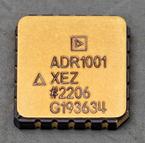
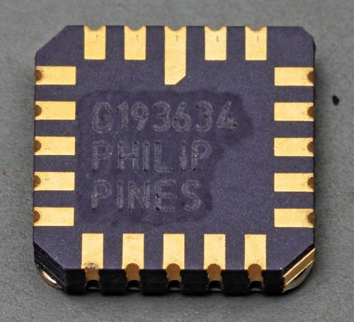
With the ADR1000 (
https://www.richis-lab.de/REF19.htm), Analog Devices has developed a successor to the extremely stable LTZ1000 voltage reference (
https://www.richis-lab.de/REF03.htm). Both the LTZ1000 and the ADR1000 require a sensibly designed, very stable external circuit. With the ADR1001 shown here, Analog Devices offers an alternative that contains all necessary circuit parts and directly outputs a stable and precisely defined reference voltage without any special additional circuitry.
The ADR1001 is not yet officially distributed. The release date has meanwhile been postponed to the end of 2023. As the letter sequence XEZ shows, this is an early sample that was produced at the beginning of 2022.
The SMD ceramic housing simplifies integration into modern circuits, but also brings disadvantages when high demands are placed on stability. Distortions of the PCB are transferred more strongly to the reference than with a TO package. The more solid connection itself can lead to mechanical stress. It is also more difficult to thermally isolate the component from the environment.
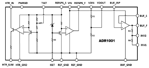
There is no publicly available datasheet for the ADR1001 yet. One can just find screenshots of a product presentation, which, however, already contain a block diagram.
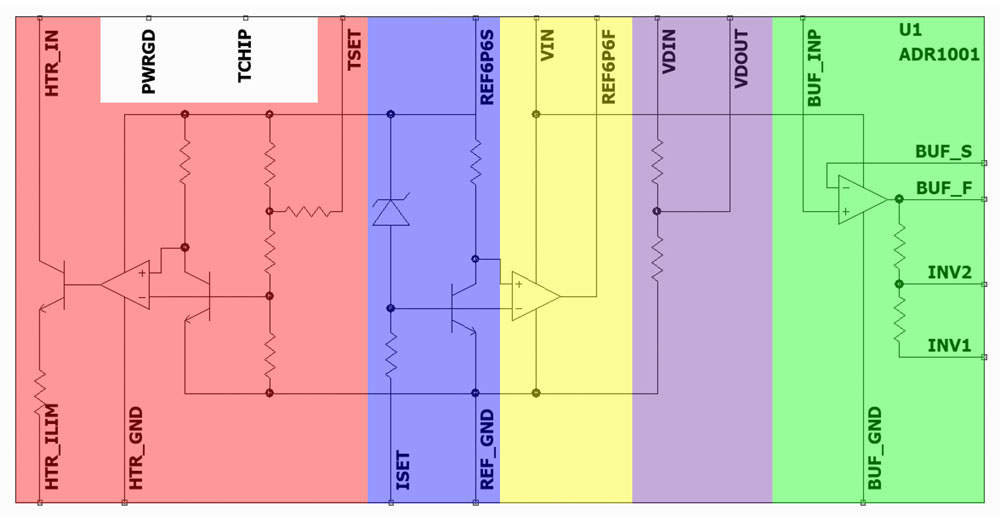
LTspice already contains a model of the ADR1001, which also shows the internal circuitry. The reference voltage is therefore based on the same circuit as found in the LTZ1000 and the ADR1000. The different temperature coefficients of a Z-diode and the base-emitter junction of a transistor (blue) compensate each other. The opamp that supplies the reference is integrated into the ADR1001 (yellow).
A voltage divider scales the initial reference voltage to 5V (purple). This facilitates integration into a circuit. Although the initial reference voltage is very constant, its absolute value is subject to relatively strong production fluctuations. The ADR1001 also contains an output amplifier (green) which, with the resistors integrated there, makes it possible to buffer the 5V reference voltage or scale it up to 10V. Allegedly, the design allows an inversion to -5V too. A separate pin to the reference potential reduces the risk of feedback from the output opamp to the reference.
In addition to the reference section, the ADR1001 contains a heater that keeps the circuit at a constant temperature (red). This has the advantage that not only the temperature of the reference itself is constant, but also the temperature of the other integrated circuit parts. Whereas with an ADR1000, for example, you have to use external resistors with a very low temperature coefficient, the temperature coefficient of the resistors integrated in the ADR1001 is much less critical.
The heater consists of the actual heating elements and a controller. The opamp in the controller uses the temperature drift of a transistor to measure the temperature and compares its base-emitter voltage with the voltage of a voltage divider. The voltage divider and thus the set temperature can be influenced via the pin TSET.
Surprisingly, according to the circuit diagram, the voltage regulator is supplied by the non-buffered reference voltage. Although the temperature regulator should have a very constant current consumption in the steady state, there is a danger here that the reference voltage will be disturbed. Both the controller and the heater have their own connection to the reference potential.
The output PWRGD obviously indicates "Power Good". According to the designation, the pin TCHIP outputs the temperature of the die. However, this designation is only found in the LTspice model, not in the block diagram.
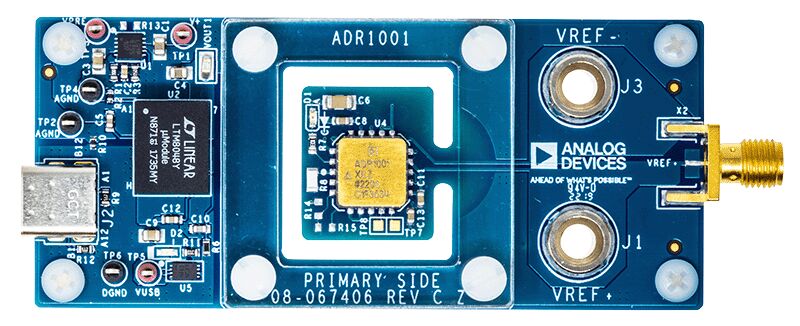
The search function on the Analog Devices website does not provide any information on the ADR1001. However, if you use an external search engine, you will find a page that advertises an Eval Board with the ADR1001.
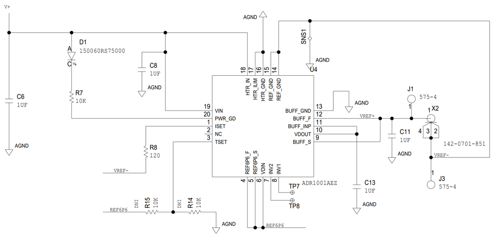
A circuit diagram is shown for the Eval board, which shows what a typical application might look like.
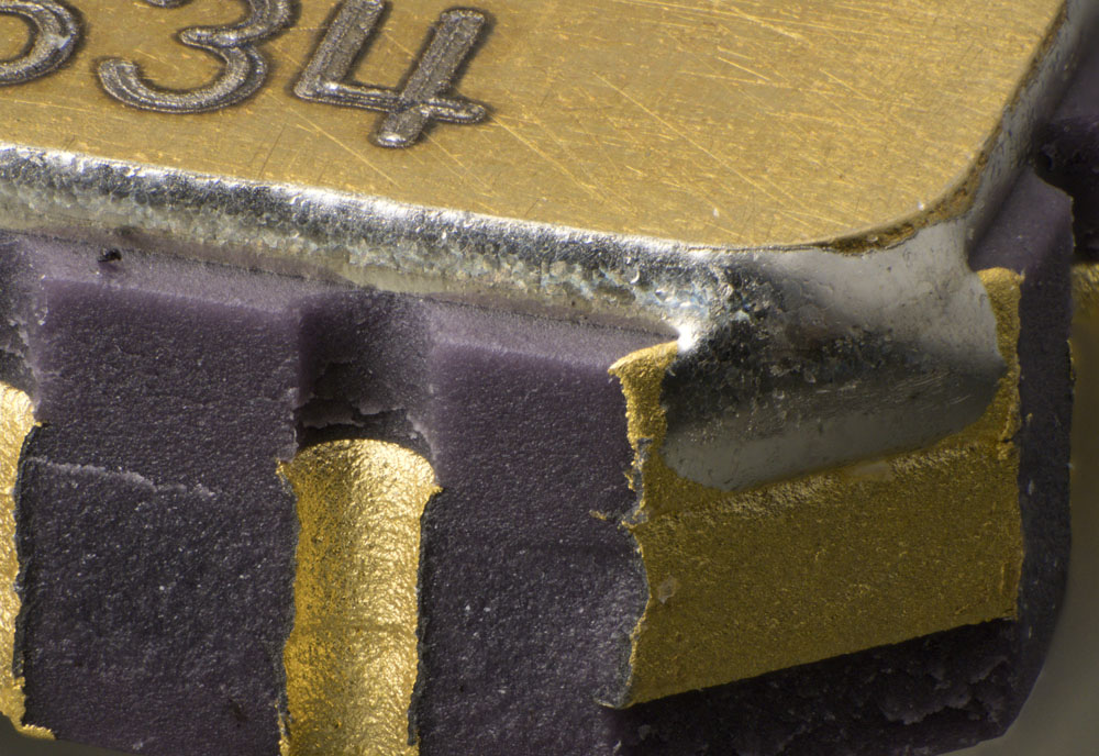
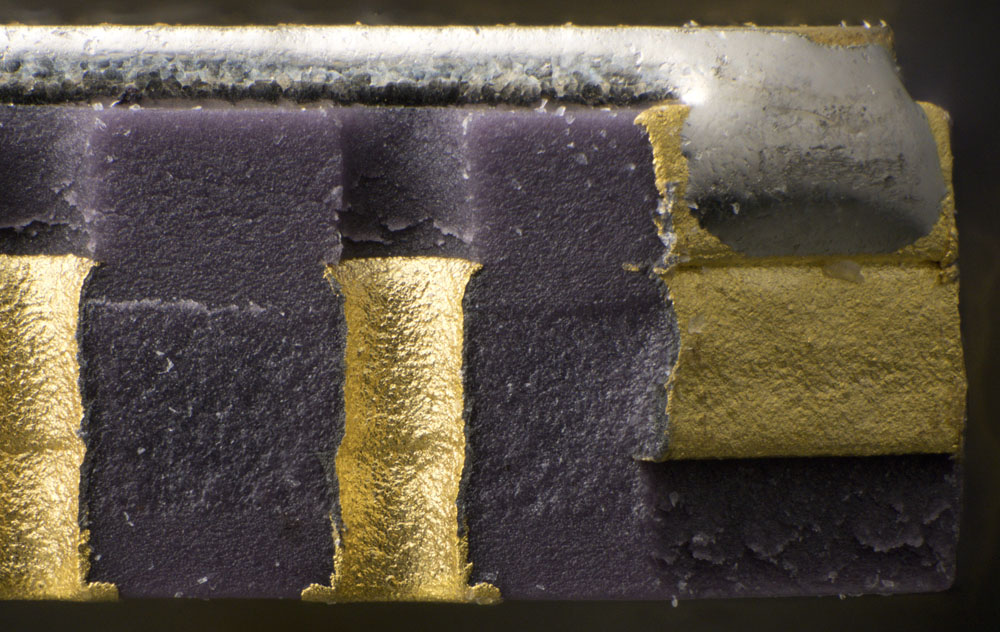
The lid of the ADR1001 is soldered to the ceramic housing. Viewed from the side, one can clearly see the layered construction. The lid is soldered to a contact in the corner of the housing that does not lead to the underside and is thus normally not electrically connected.
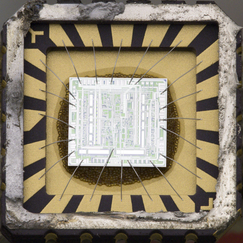
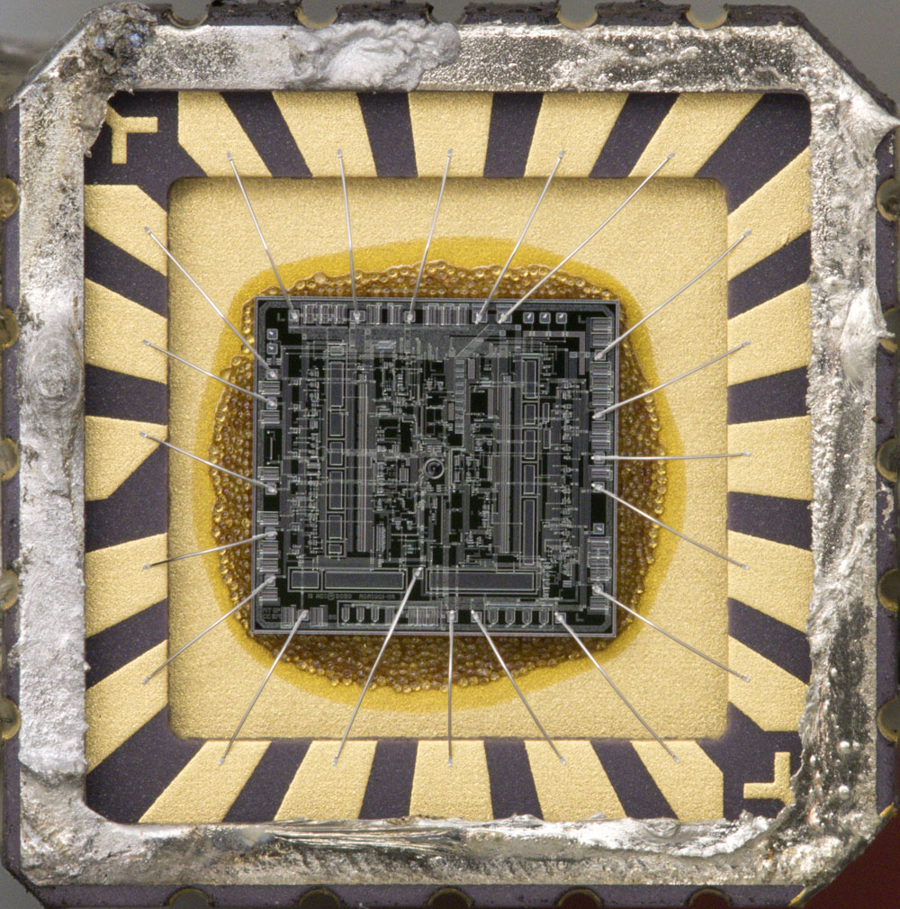
In the housing, it becomes apparent that the ADR1001 has indeed been fully integrated onto one die. Considering the high demands and the special structure of the reference element, this is not a matter of course.
As you can already guess here, the die is not conductively connected to the metallised base. No other connection to the base has been created either. This means that the potential of lid and base is floating. The surfaces form a relatively large capacitance to the die, so that interference from outside can couple into the circuit.
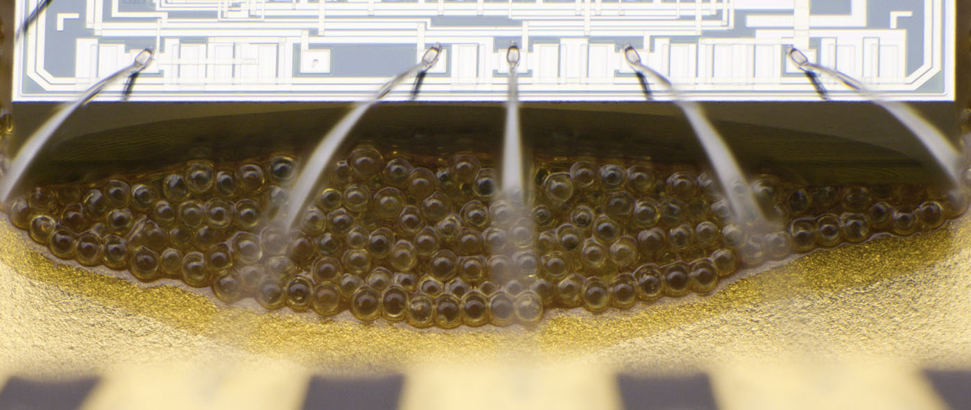
As in the LT1088 (
https://www.richis-lab.de/LT1088.htm) and the LTZ1000A, a special material was used to bond the die in the housing. It is a polymer with small glass beads. The glass beads provide a high thermal resistance between the integrated circuit and the housing. Since less heat is thus emitted to the environment, the ADR1001 reaches its set temperature more quickly and requires less heating power. This measure makes particular sense here, as the ceramic housing is connected to the circuit board over a large area. The polymer probably also helps to protect the die against mechanical stress. A polymer was also used in the ADR1000, but without an additional admixture.
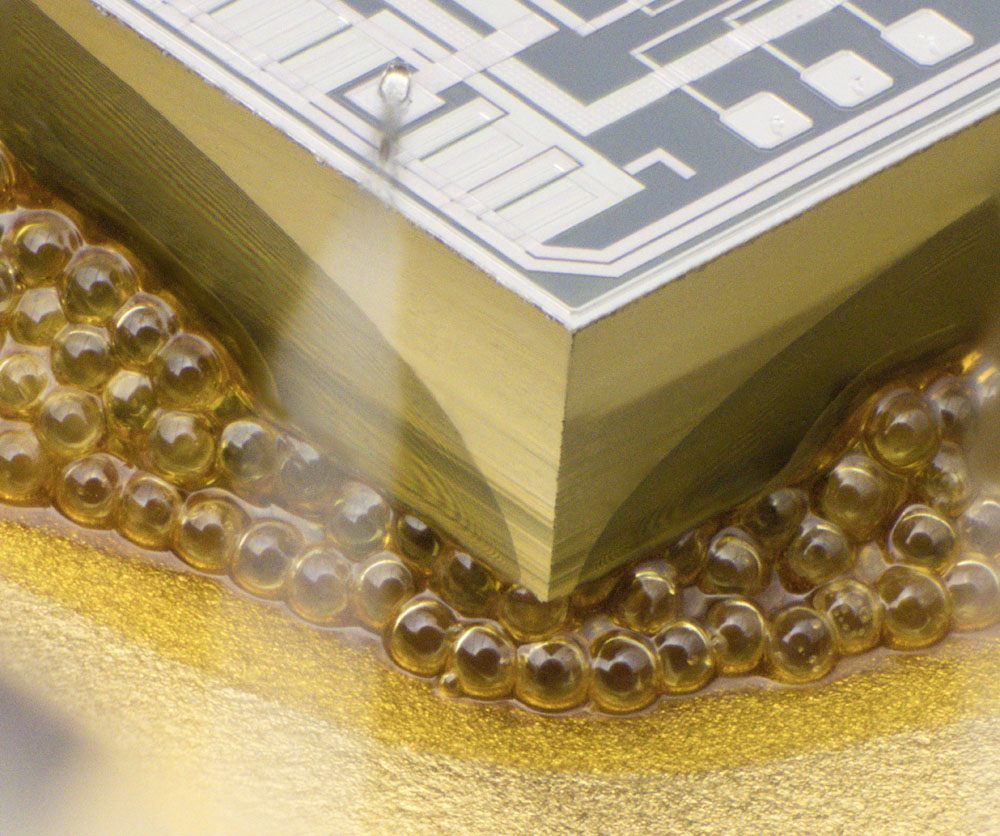
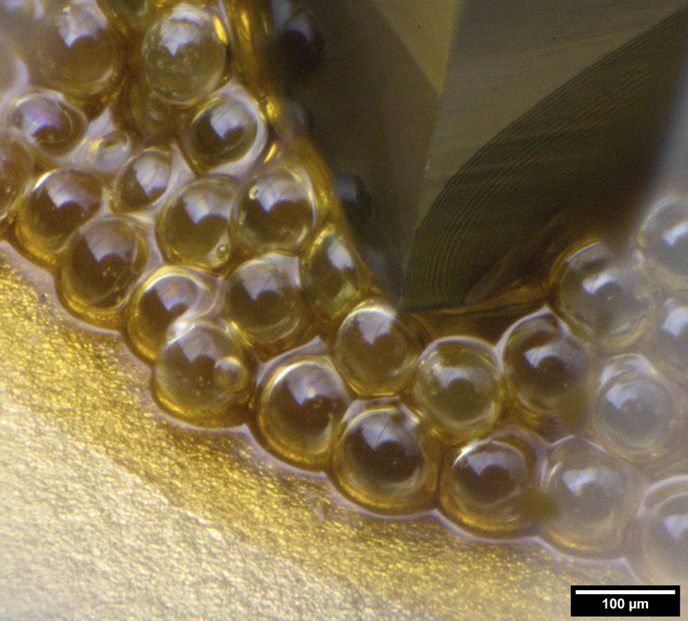
The glass beads have a diameter of about 0,1mm. The layer under the die appears to consist of two layers of the beads, so should be slightly less than 0,2mm high.
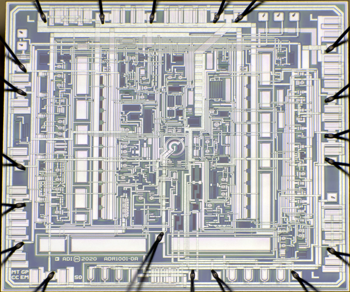
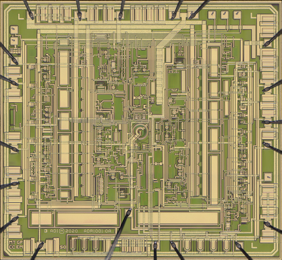
The dimensions of the dies are 3,6mm x 3,3mm. Both the top and bottom images are available in higher resolution:
https://www.richis-lab.de/images/REF01/32x14x.jpg 6,59MB
https://www.richis-lab.de/images/REF01/32x15x.jpg 56,6MB
The ADR1001 is not yet extremely highly integrated, but like the ADR1000, it has two metal layers, making it difficult to analyze the circuit.
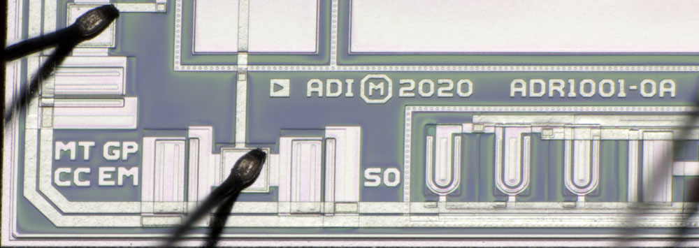
The design is obviously from 2020, and the pairs of letters are almost certainly initials of the developers involved.
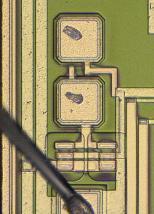
In the upper left corner of the die there is a small test structure. Two transistors are connected in parallel. The emitters are connected to ground, base and collector can be contacted via testpads. Between them a resistor is integrated, which is visually hardly noticeable between the testpads.
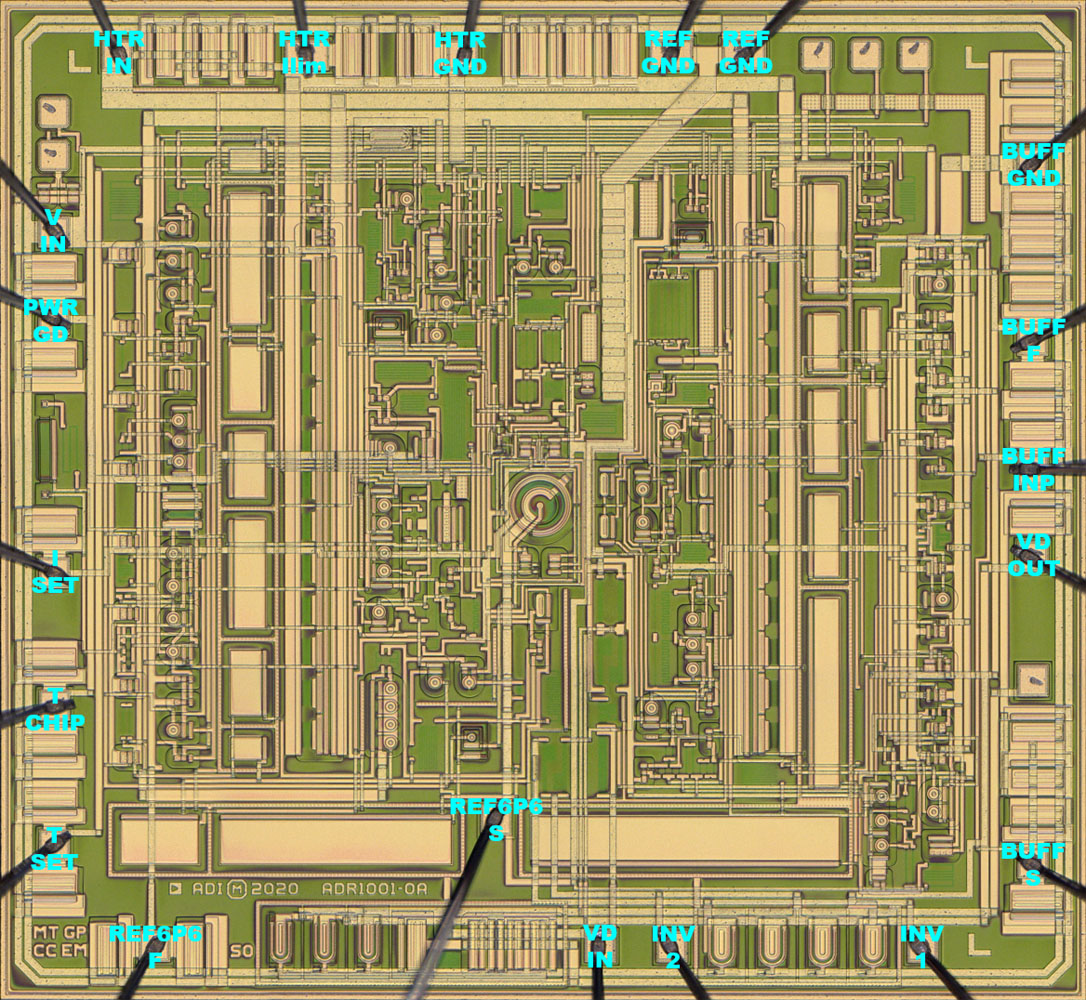
The die has 20 bondpads, all of which are assigned to a pad on the housing. In addition to the two testpads of the test structure, there are four further testpads which are used for an adjustment of the circuit.
The reference potential REF6P6_S is tapped a little further inside the die. All other potentials contact their potentials in the outer area, where protective structures are located.
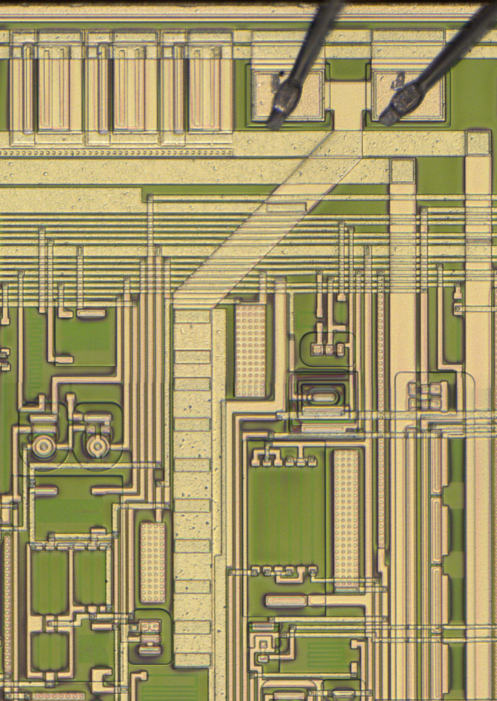
Two pads of the housing are used to transfer the ground potential. These are led to the die with two bondwires and are connected to each other there. The use of two pads and two bondwires reduces the resistance in the ground path. The relatively high temperature coefficient of the resistors is particularly problematic.
Among other ways the ground potential is transmitted in addition to the supply potential via the outer edge of the die. Particularly noticeable is the wide line, which is led diagonally downwards to the center of the die. A surprising number of large vias were used for the change from the lower to the upper metal layer.

A large part of the circuit can be identified on the die. In the center is the combination of Z-diode and transistor with its typical geometry known from the ADR1000 (blue). Unlike the block diagram, there is no resistor in the ISET path. Instead, there is an element in this path that could be a current sink.
To the right and left of the reference, large vertical strips are integrated, which consist of a series of resistors and transistors (red). These are the heaters for the temperature control of the ADR1001. The controller itself occupies a relatively large area above the reference. Large capacitors are integrated on the outside of the heaters and on the lower edge of the die. Some of the capacitors are accessed by the temperature controller. The temperature controller uses some tuned resistors. For this there are three testpads in the upper right corner. The output TCHIP is directly connected to the base-emitter junction of an otherwise isolated transistor (red/cyan).
The output buffer is clearly visible (green). The sensitive input stage is located between the reference and the right heater. The output stage, on the other hand, is on the edge, where there is less danger of it negatively affecting the reference. The opamp uses a considerable amount of the capacitors. The tuned resistors belonging to the output buffer are located near the center of the die, where the temperature is very constant.
The voltage divider, which is used to scale the reference voltage to 5V, is also tuned and is located in the center (purple). For the adjustment of these resistors a testpad is integrated at the right edge of the die.
The opamp supplying the reference (yellow) is also divided into two parts. The elements belonging to the input stage cannot be clearly identified, but they are located between the left heater and the reference, as one would expect. The output stage of the opamp is integrated between the left heater and the edge.
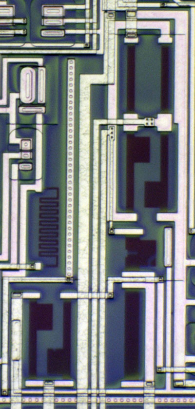
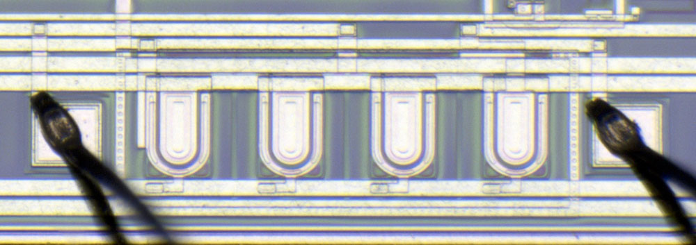
The two voltage dividers show the known traces of an alignment. In addition, there are two structures at the lower edge consisting of three and four elements, respectively, which are connected to the voltage dividers. The purpose of these structures remains unclear.
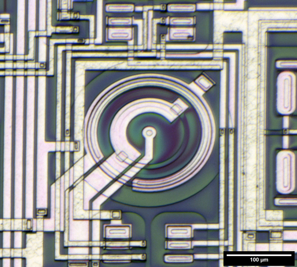
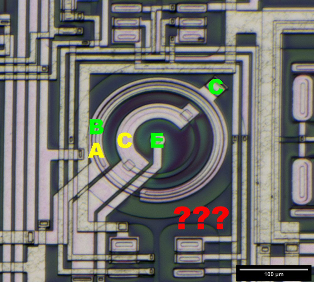
The structure in the center of the die strongly resembles the combination of Z-diode and transistor known from the LTZ1000 and the ADR1000. What seems absolutely logical at first glance raises questions when you recall the structure of this device.
As shown in the ADR1000, the base of the transistor contacts the substrate. The emitter potential is thus more negative than the substrate. In the LTZ1000 and in the ADR1000 this is not a problem, because there are no additional circuit parts on the die apart from a transistor for temperature measurement and a heater resistor.
In the ADR1001, however, a very extensive circuit is integrated on the same die. In addition, the emitter of the Z-diode/transistor combination is connected to further circuit parts. Either the reference structure in the ADR1001 is designed differently than in the ADR1000 or a process was used in which the active structures are completely isolated from the substrate.
The multiple collector connection known from the LTZ1000 and the ADR1000 is not found here. The only contact leading to the collector layer is found at the top right. Surprisingly, the collector is connected to the base of the transistor structure.
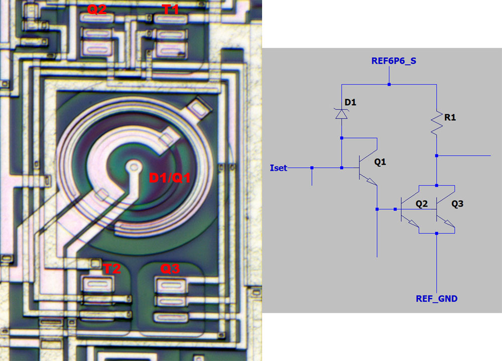
Around the combination of Z-diode and transistor there are four more transistors. Two of the transistors (T1/T2) are used for temperature control. The other two transistors (Q2/Q3) seem to have a functional part in the voltage reference and represent the branch that one would actually look for within the special structure.
https://www.richis-lab.de/REF29.htm 

 Home
Home Help
Help Search
 Login
Login Register


 Topic: ADR1001 - Ovenized Voltage Reference System (Read 317039 times)

 -->
-->