They describe it as "chopper stabilized" in the datasheet. If you think about it, the part S1, gm1, gm2, S2 is a chopper amplifier: S1 chops the differential input voltage into a square wave, the linear transistors amplify the square wave, and S2 demodulates it back into DC by sampling the peaks. To avoid differential subtraction of peaks and valleys at this point, gm3 works as a DC servo of sorts and ensures that the valleys are fixed near some internal "ground" potential.
The output of the chopper feeds gm4 and gm5, which provide additional gain. And the whole chopper is bypassed at frequencies near the chopping frequency and above in order to reduce aliasing artifacts and achieve GBW much higher than the chopping frequency.
Of course the "auto zero" explanation about gm3 canceling gm1 offset voltage and a bunch of sample-and-hold circuits making it all work is valid too. I'm not sure what the difference between "chopper stabilized" and "auto zero" is supposed to be, and if there is any real difference at all. Maybe it's only marketing talk.
I have read some articles and it seems that (today) it is common sense that "Auto Zero" is used for sampling circuits which meassure the offset and subtract it from the amplified signal. "Chopper" is used for for circuits that modulate and demodulate the signal and so loose the offset on the way. But the naming is mixed up a lot...

You are right, the sampling circuit is somehow a modulation too but in my view it´s a lot more a sampling thing.
"Stabilized" (chopper or auto-zero) means that there is a high frequency path parallel (at least that is what the articles said I have read).
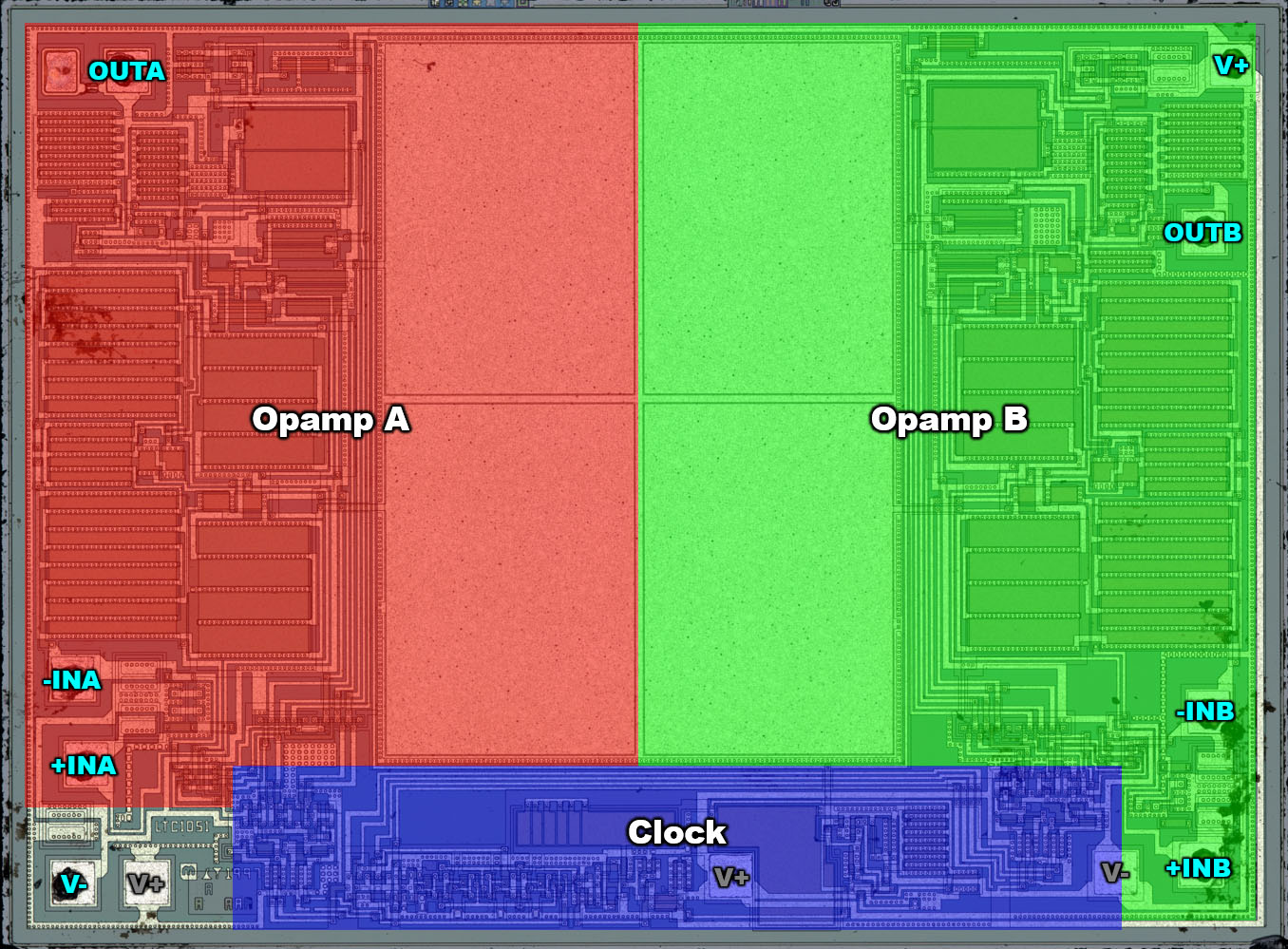
There are three unused bondpads in the lower area. These are additional options for connecting the supply potentials.
It's probably same thing as with MCP6024: two dual dice can be installed together to realize a quad. The top die gets its V+ in bottom left and V- in bottom right. The bottom die is rotated 180° so its supply connections are swapped.
I suppose it works out cheaper than designing a quad die and disabling half of it for the dual 
A good explanation!

The circuit corresponds to the block diagram in the LTC1052 datasheet. The datasheet states that the amplification factors of the amplifiers gm1 and gm6 must be as equal as possible for proper function. Furthermore, these are the amplifier stages with the high amplification factors. Accordingly, these two sections are relatively large and have the same structure.
These things look like ordinary PMOS differential pairs with PMOS current sources in the middle between gm1 and gm6 and NMOS current mirrors.
Hmm, how far are you from a complete transistor level schematic of this opamp?
The circuit is not very complex and the complete schematic would be near but I somehow don´t like MOSFETs...


 Recent Posts